Protuberant Electrode Structures for New Retinal Implants †

 ,
,
Abstract
:1. Introduction
2. Materials and Methods
2.1. FEM Simulation
2.2. Microfabrication
2.3. Implantation
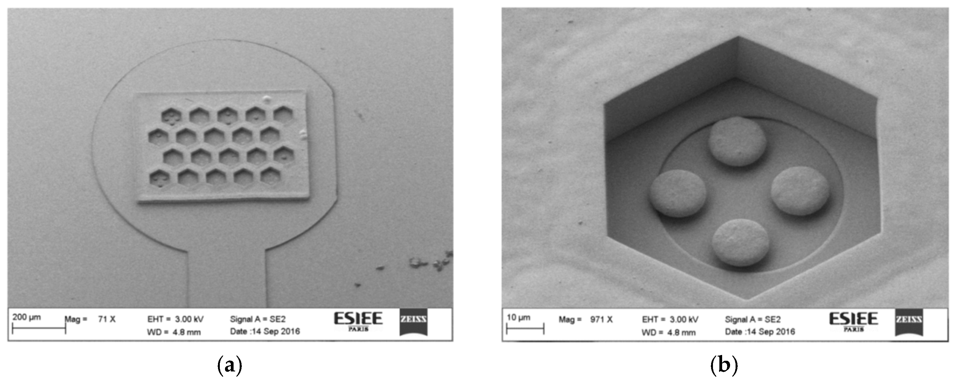
3. Results
3.1. FEM Simulation
3.2. Microfabrication
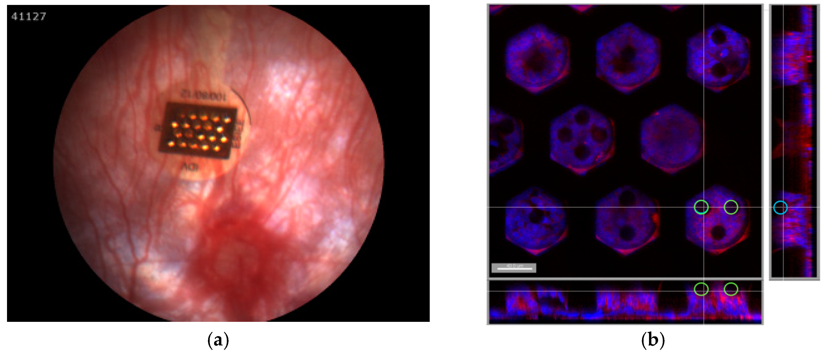
3.3. Implantation
4. Conclusions
Acknowledgments
Conflicts of Interest
References
- Joucla, S.; Yvert, B. Improved focalization of electrical microstimulation using microelectrode arrays: A modeling study. PLoS ONE 2009, 4, e4828. [Google Scholar] [CrossRef] [PubMed]
- Djilas, M.; Olès, C.; Lorach, H.; Bendali, A.; Dégardin, J.; Dubus, E.; Lissorgues-Bazin, G.; Rousseau, L.; Benosman, R.; Ieng, S.; et al. Three-dimensional electrode arrays for retinal prostheses: Modeling, geometry optimization and experimental validation. J. Neural Eng. 2011, 8, 046020. [Google Scholar] [CrossRef] [PubMed]
- Huys, R.; Braeken, D.; Van Meerbergen, B.; Winters, K.; Eberle, W.; Loo, J.; Tsvetanova, D.; Chen, C.; Severi, S.; Yitzchaik, S.; et al. Novel concepts for improved communication between nerve cells and silicon electronic devices. Solid State Electron. 2008, 52, 533–539. [Google Scholar] [CrossRef]


| Material | Conductivity (S/m) | Relative Permittivity |
|---|---|---|
| Physiological liquid | 1.47 × 10⁻² | 81 |
| Insulating material | 1.31 × 10⁻¹⁸ | 3.4 |
| Conductive material | 45.6 × 10⁶ | - |
| Electrode | Ground Plane | |||
|---|---|---|---|---|
| Wafer | Time [min] | Thickness [um] | Time [min] | Thickness [um] |
| W1 | 17 | 3.25 | 57 | 23.00 |
| W2 | 17 | 3.20 | 50 | 22.00 |
Publisher’s Note: MDPI stays neutral with regard to jurisdictional claims in published maps and institutional affiliations. |
© 2017 by the authors. Licensee MDPI, Basel, Switzerland. This article is an open access article distributed under the terms and conditions of the Creative Commons Attribution (CC BY) license (https://creativecommons.org/licenses/by/4.0/).
Share and Cite
Losada, P.G.; Rousseau, L.; Grzeskowiak, M.; Degardin, J.; Berhanu, S.; Dubus, E.; Picaud, S.; Lissorgues, G. Protuberant Electrode Structures for New Retinal Implants. Proceedings 2017, 1, 315. https://doi.org/10.3390/proceedings1040315
Losada PG, Rousseau L, Grzeskowiak M, Degardin J, Berhanu S, Dubus E, Picaud S, Lissorgues G. Protuberant Electrode Structures for New Retinal Implants. Proceedings. 2017; 1(4):315. https://doi.org/10.3390/proceedings1040315
Chicago/Turabian StyleLosada, Pedro González, Lionel Rousseau, Marjorie Grzeskowiak, Julie Degardin, Sarah Berhanu, Elisabeth Dubus, Serge Picaud, and Gaëlle Lissorgues. 2017. "Protuberant Electrode Structures for New Retinal Implants" Proceedings 1, no. 4: 315. https://doi.org/10.3390/proceedings1040315