1. Introduction
In 1956 the porous silicon was discovered by Uhlir, later for the decade of the 70’s and 80’s it is applied to chemical sensors, however until 1990 Leigh Canhan discover the luminescence at room temperature and explained it in terms of quantum confinement. There have been several studies and various applications, mainly optical sensors and biomedical applications among others [
1]. In many works have been reported the properties of porous silicon with different materials. Nowadays, the carbon nanotubes (CNTs) are very studied because of the properties that the nanostructured form and the hybridization
present. In this work, we have deposited MWCNT’s on PSi, which were dispersed by spin coating on different PSi single layers with different anodizing parameters. The optical and morphological properties of PSi in the c-Si-n/PSi and Al/c-Si-n/PSi/MWCNT/SiOx/Al structures are studied and analyzed.
2. Materials and Methods
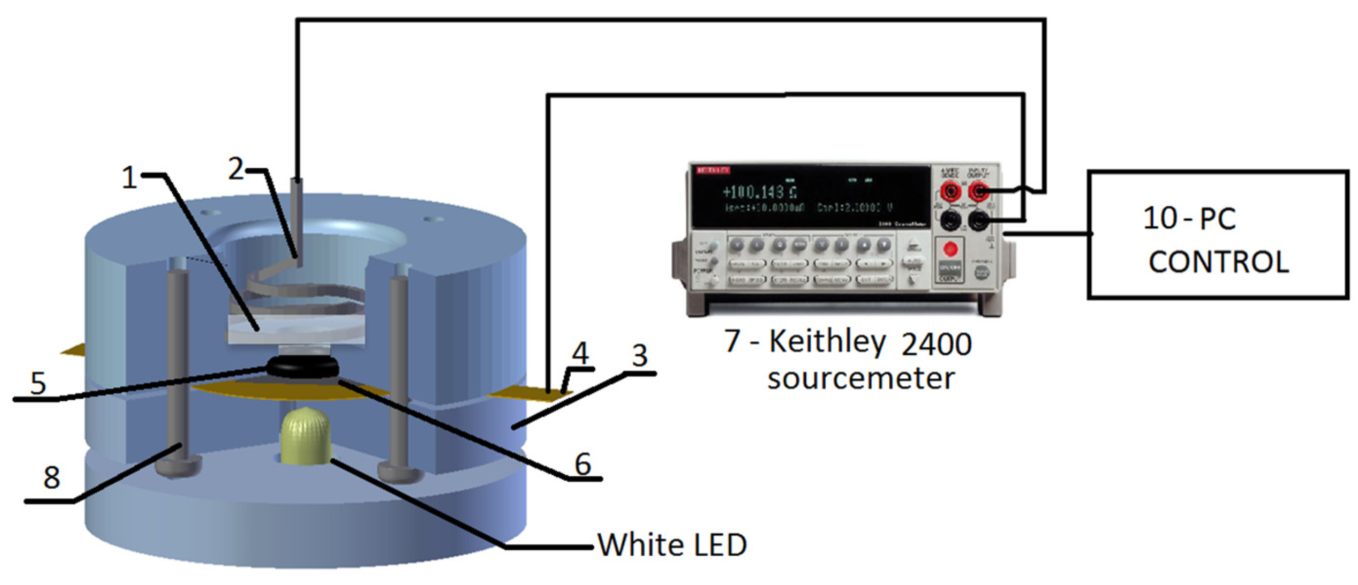
PSi was obtained by electrochemical anodization of <100> n-type c-Si wafers with low resistivity (<0.005 Ω·cm). Such process was carried out with the experimental setup shown in
Figure 1. The electrolyte used in this experimental setup contained
in a proportion of 6:3:1 by volume, the applied currents were the following 10, 50 and 100 mA in an area of 1.32 cm
2. A white LED was used as light radiation source in order to trigger the electron photo-generation which is necessary to supply holes for the formation of pores and also to reduce other undesirable light sources. The process was realized under dark conditions. The experimental arrangement is shown in
Figure 2.
To study the effects of MWCNTs dispersed in the monolayers of PSi it was necessary to deposit them on PSi. The deposition of the MWCNTs was carried out by the spin coating technique; 10 drops were placed on the sample at 3000 rpm for 15 s, rising the spinning at 5000 rpm to infiltrate them, this process was repeated 5 times since previous research confirms a greater presence of CNT that reduces the sheet resistance in the monolayer. MWCNTs with lengths ranging from 2.5 to 4.5 micrometers and outer diameters between 15 and 25 nm were used. With the thermal oxidation in a tubular furnace at T = 300 °C, along with a flow of O2 at 5 mL/min, the surface of the PSi layer is expected to be passivated. Through the oxidation process, chemical bonds are generated in such a way that MWCNTs are better anchored to the PSi layers grown. We have finally a phase composition material of SiOx, CNTs, PSi, and c-Si forming a complex structure.
3. Results and Discussion
The porosity and thickness of PSi monolayers were determined by gravimetric analysis. The porosity is given by
where
is the wafer weight before the electrochemical etching,
just after the one and
is finally when the porous layer has been removed from substrate, and with the equation
we obtain the PSi monolayer thickness, where
is the anodized surface and
is the silicon density [
3].
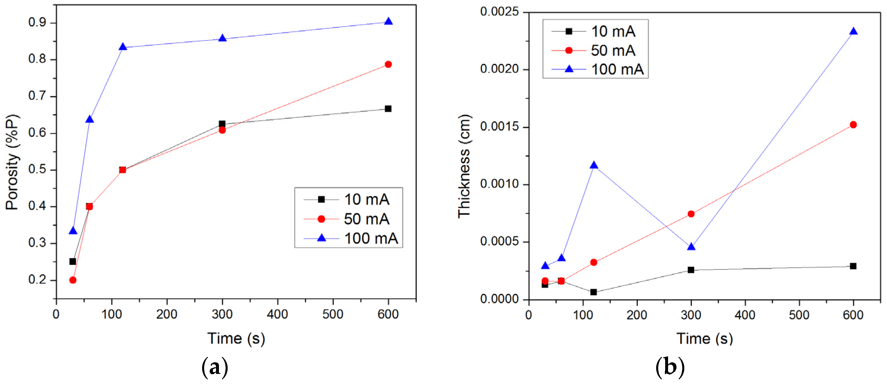
The porosity and thickness values are plot in
Figure 3. At a fixed current the porosity increases as the anodizing time increases, while keeping the anodizing time fixed and varying the anodizing current it is observed that the greater current, the greater the porosity except for anodizing times in the range 50–300 s for 10 mA and 50 mA currents where porosity overlap with constant values. The thickness in
Figure 3b shows a similar general behavior although for 100 mA, thickness decreases abruptly at 300 s.
SEM micrographs in
Figure 4 confirm the deposition of the MWCNTs on thermally oxidized PSi surfaces, also mesopores of different diameters are observed, which depend on the applied current with values of 10 mA, 50 mA, and 100 mA. These SEM micrographs confirm the fact that the higher currents are applied in the etching process the larger pore sizes are obtained.
Reflectance spectra of c-Si-n/PSi-n/MWCNT/SiOx structures in
Figure 5a present the typical Fabry-Perot oscillations due to the different PSi layer thicknesses, standing out the decreasing amplitude as consequence of the increased porosity [
4,
5,
6]. According to
Figure 5b, the presence of the MWCNTs affects mainly the spectrum associated with the lowest anodizing time (0.5 min), in the region from 400 to 750 nm, the oscillations are attenuated. The reasons contributing to this drop may be originated from the coated PSi surface by the MWCNTs dispersed which generates light trapping and it hinders light be reflected.
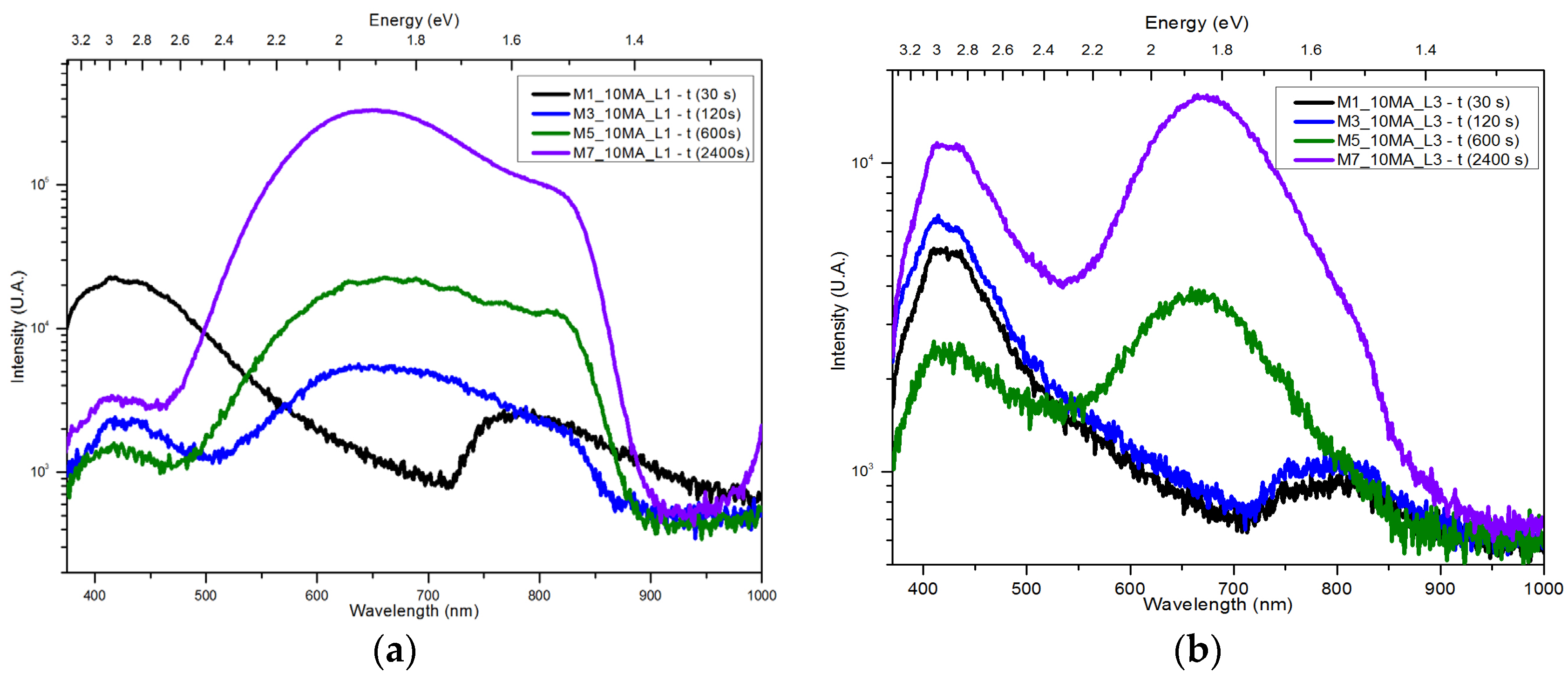
Spectra of photoluminescence shown in
Figure 6a, were obtained from the PSi samples without MWCNTs. These ones were obtained with anodization times between 0.5 min and 40 min. They show bands in the UV and red region whose amplitudes are inverted for bigger anodization times.
Figure 6b shows Photoluminescence spectra with present MWCNTs and thermal oxidation realized after MWCNTs deposition. There is a clear tendency to form two main bands in the UV and red regions according as the anodizing time is increased. Predominantly the influence of Si-O, SiHx and Si-OH bonds determine the luminescence spectra shape and to a less extent the influence of the creation of a hydrogen-carbon surface between the carbon atoms on the MWCNTs and the hydrogen-Si on PSi layer [
1,
6].
4. Conclusions
PSi samples without and with MWCNT were obtained and prepared. The results showed that when the anodization time and electrical current are increased, the samples porosity also increased. SEM micrographs showed that for large currents the diameter pore size increased on the PSi monolayer, also the MWCNTs have been dispersed horizontally on PSi surface by using spin coating technique.
Photoluminescence spectra obtained exhibit the apparition of two main bands in the UV and red regions such fact indicates that our structures studied may be focused to be applied in sensors and solar cells.
Author Contributions
N.V.H. and J.A.L.L. conceived and designed the experiments; N.V.H. and E.G.B. performed the experiments; N.V.H., J.A.L.L., M.A.D.J. analyzed the data; N.V.H., J.D.A.H.d.l.L., E.G.B. and J.A.L.L. wrote the paper. All authors have read and agreed to the published version of the manuscript.
Acknowledgments
This work has been partially supported by CONACyT-CB-255062 and VIEP-LULJ-EXC-2017. The authors acknowledge CIDS, INAOE and IFUAP laboratories for their help in the samples characterizations. The authors thank Norma Mendoza and the McGill University for supplying MWCNTs for the present work.
Conflicts of Interest
The authors declare no conflict of interest.
References
- Gelloz, B. Photoluminescence of Porous Silicon. In Handbook of Porous Silicon; Canham, L., Ed.; Springer International Publishing: Gewerbestrasse, Switzerland, 2014. [Google Scholar] [CrossRef]
- Jarimavičiūtė-Žvalionienė, R.; Grigaliūnas, V.; Tamulevičius, S.; Guobienė, A. Fabrication of Porous Silicon Microstructures using Electrochemical Etching. Mater. Sci. 2003, 9, 317–320. [Google Scholar]
- Concepción Arenas-Arrocena, M.; Vega-Gonzalez, M.; Martinez, O.; Salinas-Aviles, O.H. Nanocrystalline Porous Silicon: Structural, Optical, Electrical and Photovoltaic Properties. In Crystalline Silicon—Properties and Uses; Basu, S., Ed.; InTech: Rijeka, Croatia, 2011; p. 254. [Google Scholar] [CrossRef]
- Jane, A.; Dronov, R.; Hodges, A.; Voelcker, N.H. Porous silicon biosensors on the advance. Trends Biotechnol. 2009, 27, 230–239. [Google Scholar] [CrossRef] [PubMed]
- Hordy, N.; Mendoza-Gonzalez, N.-Y.; Coulombe, S.; Meunier, J.-L. The effect of carbon input on the morphology and attachment of carbon nanotubes grown directly from stainless steel. Carbon 2013, 63, 348–357. [Google Scholar] [CrossRef]
- Olenych, I.B.; Aksimenyeva, O.I.; Monastyrskii, L.S.; Horbenko, Y.Y.; Yarystska, L.I. Sensory properties of hybrid composites based on poly (3,4-ethylenedioxythiophene)-porous silicon-carbon nanotubes. Nanoscale Res. Lett. 2015, 10, 187. [Google Scholar] [CrossRef]
| Publisher’s Note: MDPI stays neutral with regard to jurisdictional claims in published maps and institutional affiliations. |
© 2017 by the authors. Licensee MDPI, Basel, Switzerland. This article is an open access article distributed under the terms and conditions of the Creative Commons Attribution (CC BY) license (https://creativecommons.org/licenses/by/4.0/).

 ,
, 


