
Controlling Surface Wettability and Plasmonic Resonance of Au/ZnO Heterostructured Films


Institute of Manufacturing Technology, Department of Mechanical Engineering, National Taipei University of Technology (TAIPEI TECH), Taipei 10608, Taiwan
*
Author to whom correspondence should be addressed.
J. Compos. Sci. 2022, 6(11), 328; https://doi.org/10.3390/jcs6110328
Submission received: 10 October 2022
/
Revised: 20 October 2022
/
Accepted: 31 October 2022
/
Published: 2 November 2022
(This article belongs to the Special Issue Feature Papers in Journal of Composites Science in 2022)
Abstract
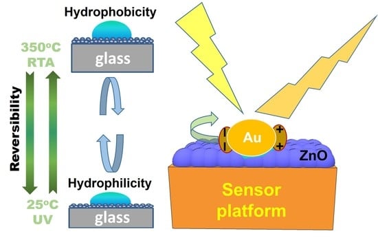
:This work investigated the (0002) textured ZnO films without and with the addition of an Au continuous top layer and its effects on their surface wettability and plasmonic resonance characteristics. The ZnO films were directly fabricated onto glass substrates at the synthesized temperature of 300 °C via a plasma-enhanced chemical vapor deposition (PECVD) system, and the as-synthesized ZnO film exhibited an average optical transmittance value of 85%. The ultraviolet (UV) light irradiation can be applied to enhance the hydrophilicity, changing it from a hydrophobic status to hydrophilic status due to the existing and adjustable characteristics of the photocatalytic activity. On the other hand, the surface wetting/contact angle (CA) value of the ZnO film with a controllable surface wettability switched from 94° (hydrophobicity) to 44° (hydrophilicity), after it was exposed to UV light irradiation for 5 min, and stably reversed back to hydrophobicity (92°) via a post-annealed treatment using rapid thermal annealing (RTA) at 350 °C for 5 min in air. A fast, simple, and reversible method for switching between hydrophilic and hydrophobic status is claimed in this present work. The improved surface plasmonic resonance is owning to the coupled electron and photon oscillations that can be obtained and produced at the interface between the flat Au layer and ZnO (metal/metallic oxide) heterostructured films for future applications of various wide-bandgap compound semiconductors.
1. Introduction
A wide range of works in surface wettability and related surface plasmonic resonance of wide-bandgap compound semiconductors have been attractive for various powerful applications, for example, as photodetectors, biosensors, energy harvesters, and related optoelectronic nanogenerators [1,2,3,4,5,6,7,8,9,10,11,12]. Many multifunctional detectors and sensors have been attractive, due to their one-dimensional (1-D) nanoparticles, and have exhibited difficult questions for their large scale use in the uniform process of producing goods. The surface treatment onto substrates is a simple and fast technique to achieve remarkable surface plasmonic resonance characteristics in the coupled optoelectronic capabilities connected with the underlaying platforms [13,14,15,16,17]. The powerful exciton–plasmon coupling in the metal capping layer combined with semiconducting oxides has potentially supplied a technique to strengthen the exciton–plasmon interaction and related particularity for various applied fields [18,19,20]. The hydrophobic/hydrophilic surface treatments have been controlled by adjusting the surface state via low/high surface energy to produce nano/micro-structured morphology. One of the wide-bandgap compounds, ZnO, is a famous choice for photocatalysis among the semiconductors. ZnO exhibits photocatalytic activity under ultraviolet (UV) light irradiation due to its large bandgap, its surface wettability can be usefully controlled by UV light irradiation [21,22,23,24,25], and the multifunctional ZnO phase is a good choice for self-cleaning surface-coating treatment. The reversible hydrophobicity/hydrophilicity driven by UV light in ZnO-based composited compounds has been widely applied and confirmed [26,27,28,29]. Therefore, the wide-bandgap ZnO compound can be used in UV photodetectors, piezoelectric transducers, light-emitting diodes, transparent thin film transistors, photovoltaic cells, semiconducting gas sensors, biomedical sensors, and so on [30,31,32,33,34,35].
Due to the above various applications, ZnO has a controllable surface effect, which can offer a remarkable surface wettability and reversible hydrophobic/hydrophilic transformation by using UV light irradiation generated from its intrinsic semiconductor character. It can be understood that the reversible wettability of the ZnO compound was due to the competition of surface chemical characteristics between adsorption and desorption of the rearrangement of hydroxyl groups and organic supply chains on its surface state [36,37,38]. The photo interactive ZnO has been highly used to display controllable wettability, combining rapid hydrophobic/hydrophilic switching with a controllable contact angle. On the other hand, many fabricated methods on controlling microstructures have been described, which are developed to control the wettability of various functional films. There are various fabricated ways ZnO films have been described, for example, in thermal evaporation, laser molecular bean epitaxy (MBE), pulsed-laser deposition (PLD) with high-power energy, metalorganic vapor phase epitaxy (MOVPE), radio-frequency magnetron sputtering, and plasma-enhanced vapor chemical deposition (PECVD) [39,40,41,42,43,44,45,46,47]. The PECVD method is suitable for manufacturing large-area uniform ZnO films for the purpose of applying them in future optoelectronic nanodevices and biosensors because it has attracted important attention due to its stable deposition rates and rapid growth of high-quality films. It is well known that the synthesized uniformity of thin/thick films with a large area is caused by various synthesized conditions including synthesized pressure, synthesized temperature, synthesized power, and the distance between the precursor sources and substrate.
This work offers a fast, simple, and reversible way to control the surface wettability of ZnO films from hydrophobicity (94°) to hydrophilicity (44°) by exposing them to UV light irradiation at room temperature for 5 min and stably reversing them back to hydrophobicity (92°) via a post-annealed treatment using rapid thermal annealing (RTA) at 350 °C for 5 min in air. The coupling of surface plasmons and excitons using Au/ZnO heterostructured films has been used to investigate the coupling influence of the metal/metallic oxide heterostructures. This not only offers the potential requirements of ZnO films but also provides a simple way with a wide-bandgap compound semiconductor and the related evolution of flexible and transparent nanodevice development.
2. Experiments and Film Structures
The ZnO films were synthesized onto Corning-1737 glass substrates by using a plasma-enhanced chemical vapor deposition (PECVD) system at a synthesized temperature of 300 °C and synthesized pressure of 5 Torr. The substrates were cleaned in acetone and ethanol at first to remove organic contaminants, then ultrasonically rinsed in deionized water, and finally dried in hot air before they were set into the synthesized chamber. The high-vacuum synthesized chamber was pumped down to a pressure of 3.5 × 10⁻⁶ torr. The argon gas and its plasma generated from a radio-frequency (RF) generator was used to purge the carbon dioxide (CO2) and diethylzinc (DEZn), which were used as precursors to supply oxygen and zinc sources, respectively [48,49,50].
The crystalline preferred orientation and crystallinity in ZnO films were examined by X-ray diffraction analysis (XRD, PANalytical, Almelo, the Netherlands) with Cu Kα radiation (λ = 1.54 Å) in the 2θ ranges of 30–50°. The scan speed was 0.01° 2θ/s during the XRD measurement with the proportional counter. The rocking curves for the characterization of the crystal perfection by means of the ω scan geometry were paired with a scan speed of 0.01° θ/s during measurement. The morphological features on the surface and corresponding elemental composition for ZnO films were analyzed by a scanning electron microscope (SEM, Phenom XL G2, Thermo Scientific, Waltham, MA, USA) and field emission scanning electron microscopy (FE-SEM, Dresden, Germany), respectively. The measurement and calculation for the contact angle and surface free energy of ZnO films were evaluated with the water wetting/contact angle (CA, Rame-Hart 100 goniometer, Capovani Brothers Inc., Scotia, NY, USA) measurement by using small drops of liquid water onto the surface of each ZnO film. The degree of accuracy of the water contact-angle measurement was induced by the image quality, using a charge-coupled device (CCD) to capture the images of the drops of liquid water (~5 μL). Then, the processing of the fitting curve function was achieved immediately by using CA software, and the value was evaluated to be approximately ±1 degree. At the same time, the related measurement of surface free energy (SFE) for each specimen could also be simultaneously evaluated. The UV light irradiation onto each ZnO specimen was exposed by a 1520 mW/cm2 mercury arc lamp (HAMAMATSU-Deuterium L2D2) with a wavelength of 365 nm, and all the ZnO specimens were stored in dark surroundings at air ambient after irradiated with UV light for 5 min. In order to investigate the plasmonic effect, a 15 nm-thick Au layer was determined to deposit onto textured ZnO films, which were denoted as Au/ZnO heterostructured films.
3. Results and Discussion
From Figure 1a–c, the plane-view and cross-sectional SEM images of the ZnO specimen clearly show a high density of hexagonal nanograins with columnar structures, respectively. The film thickness of the ZnO specimen was designed and fixed at approximately 250 nm, as shown in Figure 1b. The size of the nanograins had a basically uniform distribution at approximately 34 ± 6 nm, as shown in Figure 1d. Figure 1e shows the typical in-plane θ-2θ X-ray diffraction spectrum for the ZnO specimen. The XRD spectrum confirmed the specimen demonstrates a diffraction peak positioned at approximately 2θ = 34.2°, which corresponded to the high degree of c-axis orientation along the ZnO (0002) plane that matched well with the standard diffraction pattern of the wurtzite crystal phase (JCPDS Card: 36-1451). The significant intensity of the diffraction spectra originated from the ZnO (0002) plane and is due to the smallest surface energy in the ZnO (0002) basal plane in the wurtzite crystal structure, contributing to a crystallographic orientation along the [0001] preferred crystalline direction. It can be understood that no peak except the (0002) diffraction angle is obtained in the whole diffraction patterns (θ–2θ scan), demonstrating that the ZnO film did epitaxially synthesize onto the glass substrates. In addition, a detailed analysis of the rocking curves (ω) scan along the ZnO (0002) plane is shown in Figure 1f, and the full width at half maximum (FWHM) value of the rocking curve is 0.185°.
In general, the ZnO columnar structure with c-axis crystallographic orientation has been most commonly achieved in several fabricated skills including physical/chemical vapor deposition and wet solution methods [51,52]. Many models have been developed to describe the growth mechanism of crystalline preferred orientation, including preferential crystallographic nucleation, nucleated probability on the outermost plane, surface diffusion of atoms, and anisotropic nucleation rate of the various crystallographic planes. The above analysis demonstrates the (0002) textured ZnO films with the preferred polar c-axis orientation, which belongs to a hexagonal wurtzite structure.
Retaining the quality of the visible transmittance of the nanodevice plays a critical role in the industrial and particular applications, such as solar cells and optoelectronic panel displays. Figure 2 shows the transmission curve for the as-synthesized ZnO film compared with the Corning-1737 glass substrate, respectively. From the transmittance spectra, the as-synthesized ZnO film exhibited enough transparency with an average transmittance value of 85.4%. The equation formula to count Tavg can be described as:
where T(λ) is the transmittance of the ZnO films synthesized onto glass substrates, and λ1 and λ2 are the boundary condition of the lower border and upper border in the wavelengths of the optical measurement. It could be depicted that Tavg was counted using Equation (1) over the wavelength range from 375 to 825 nm. The columnar ZnO film with the preferred c-axis orientation that directly synthesized onto the glass substrate had excellent transparency and showed an average visible light transmittance higher than 80%. It is demonstrated that the hydrophobic (0002) textured ZnO columnar films have great potential to be applied in fields such as current smart window techniques combined with the corresponding wide-bandgap semiconducting, energy harvesting, and optoelectronic devices.
The surface wetting/water contact angle (CA) is 94° for the as-synthesized ZnO film that shows hydrophobic surface wettability due to the grain size (34 ± 6 nm) with enough apertures supply more the trapping of oxygen that reduces the contact area between water droplet and surface of ZnO film, as shown in Figure 1c and Figure 3a, respectively. For the purpose of controlling the surface wettability transition of the ZnO film, the specimen was placed under an ultraviolet (UV) light irradiation with a wavelength of 365 nm for 5 min at room temperature, which could supply a higher photon energy than the intrinsic band gap (3.37 ev) of the ZnO phase. It can be seen that the CA value of the ZnO film with UV irradiation for 5 min clearly changed from 94° to 44°, as shown in Figure 3b. In a word, the hydrophilic surface wettability could be strengthened when there is less oxygen caught between the solid and liquid surface, causing a small CA via UV light irradiation. The rapid reducing of the CA value of ZnO film can be attributed to the photocatalytic activity due to the fact that energy bandgap illumination produces electron-hole pairs in many semiconducting oxide phases by the emission of photoelectrons [53,54,55,56,57]. Then, the ZnO film with the rapid thermal annealing (RTA) treatment at 350 °C for 5 min in air was needed to reverse the initial wettability status (92°), as shown in Figure 3c. The time dependence of the CA value for the reversible hydrophobicity/hydrophilicity switch for ZnO film under UV irradiation (25 °C) and then with RTA (350 °C) is schematically shown in Figure 3d. The reversible hydrophobicity/hydrophilicity transformation of the ZnO film by alternating UV irradiation and RTA procedures could be controlled and claimed in this present work.
It can be understood that the holes and electrons can either transform or recombine into the ZnO film surface to react with groups adsorbed on the ZnO film surface. The UV light irradiated on the ZnO film and then the produced photon energy was larger than the energy bandgap of ZnO; the electrons (e−) were excited into the conduction band from the valence band. Additionally, if the same number of holes (h+) were caused in the valence band, some of the holes combined with surface oxygen atoms or lattice oxygen (O2−) to progress the surface oxygen vacancies O1−, while the electrons combined with lattice metal ions (Zn2+) to progress Zn2+ defective sites, the water molecules and oxygen would contend with each other for the purpose of absorbing dissociatively on the imperfect sites. The surface caught electrons (Zn+) to combine with the oxygen molecules adsorbed on the ZnO surface. In the interim, the water molecules could coordinate with the oxygen vacancy sites (VO), which resulted in the dissociative adsorption of the water molecules onto the surface of the ZnO film. The imperfect sites are kinetically more desirable for hydrophilic hydroxyl group (OH−) adsorption than oxygen adsorption, and the related reactions are as listed in Equations (2)–(6), which describe the generation processes of imperfect sites on the surface of ZnO films.
ZnO + 2hv → 2h+ + 2e−
Some of surface oxygen atoms or lattice oxygen (O2−) react with the holes to generate surface oxygen vacancies O1−, while some of the lattice metal ions (Zn2+) combine with electrons to generate Zn2+ imperfect sites, as described in the following equations.
O2− + h+ → O1− (surface trapped hole)
Zn2+ + e− → Zn+ (surface trapped electron)
O1− + h+ → 1/2O2 (gas) + VO (oxygen vacancy)
The oxygen and water molecules could contend with each other to absorb dissociatively on the imperfect sites. The surface caught electrons (Zn+) to combine with oxygen molecules adsorbed on the ZnO film surface:
Zn + O2 → Zn2+ + O2−
The UV irradiation could be used to control the chemical surface states of the ZnO film, and hence control its surface wettability. The above results indicate that the reversible hydrophobic/hydrophilic surface wettability of the wide-bandgap compound semiconductors, such as ZnO film, can be simply controlled by alternating UV irradiation and RTA procedures for many potential nanodevices such as biomedical sensors, bioanalytical devices, and future multifunctional nanodevices [58,59,60,61,62].
For the purpose of investigating the plasmonic coupling influence, a 15 nm-thick Au top layer was applied to grow onto ZnO films, which were denoted as Au/ZnO heterostructured films. A single Au top film existed with a continuous layered structure grown onto the ZnO film, as examined by the two-dimensional (2D) atomic force microscope (AFM) image shown in Figure 4a. The continuous growth of the top layer was also confirmed by a three-dimensional (3D) AFM image, as shown in Figure 4b. From the AFM line-scan, shown in Figure 4c, the height of the Au continuous layered structure was confirmed and observed. The X-ray scattering was applied to ideally complement these microscopic methods since it can successfully reflect representative microstructural information for a large specimen area for Au/ZnO heterostructured films, as shown in Figure 4d. The XRD pattern for Au/ZnO heterostructured films has typical ZnO(0002) and Au(111) diffraction peaks, which confirms the existence of the Au layer coated onto the ZnO films, which can be indexed to Au/ZnO heterostructured films in a crystalline phase. On the other hand, no diffraction peak from the indefinite phase from the Au/ZnO heterostructured films was obtained, thus providing strong evidence for the complete coverage of the ZnO by Au without an intermixed phase. The above morphological and structural results analysis provide the configuration of Au/ZnO heterostructured films, and the XRD spectrum analysis consists of the observation from the topical AFM images, as shown in Figure 4a,b. The plan-view SEM image of Au/ZnO heterostructured films showed a highly uniform covering status, and typically displayed flat surface morphology, as shown in Figure 4e. It can be obviously observed that the CA value of Au/ZnO heterostructured films varied from 94° (ZnO) to 80° (Au/ZnO) while coated with the Au continuous top layer, as shown in Figure 4f.
The photoluminescence (PL) spectrum is applied to be significant, as a regular method to verify the optical performance of ZnO films. The PL emission spectrum of typical ZnO film can be separated with two main components. The first component is due to near-band-edge (NBE) emission spectrum, which is contributed by the free-exciton recombination generated in the UV zone. Another one is the deep-level (DL) emission spectrum, which is constructed from the impurities and related possible defects, including oxygen vacancies and zinc interstitials, which originated from the suppression of the DL emission spectrum in the visible zone. Figure 5 shows the PL spectra of the ZnO films without and with the Au top layer, respectively. The tough NBE emission spectrum is positioned at approximately 372 nm and acts for the dominant recombination mechanism of photogenerated charge carriers (excitonic photoemission) in the pristine ZnO film. The PL quenching in the Au/ZnO heterostructured films is owing to the coupling of the light emission with the localized surface plasmonic (LSP) resonance of the Au continuous layer, as shown in Figure 5. In addition, the metallic LSP effect can trigger both interband excitation and plasmonic excitation [63,64]. The Au continuous layer associated with LSP can also cause the photoelectron process owing to its absorption cross section and localized optical intensity.
The surface plasmonic resonance (SPR) is the coupled electron and photon oscillations that can be produced and obtained at the interface between the Au metal and ZnO metallic oxide for the purpose of designing the SPR heterostructured films. It is well known that the pure metals could supply surface plasmonic collective oscillations of free electrons, which could collect the electromagnetic (EM) waves to a small fraction of a wavelength, while improving the local field energy by several times of the magnitude [65]. The local EM field experienced by analyte molecules on the metallic surface in the nanoscale is dramatically improved, generating considerably improved Raman intensity [66]. We considered that such a kind of ZnO semiconductor coated with an Au continuous top layer may induce a localized field around its surface, and there may be a coupling effect and exhibit the SPR. For the purpose of identifying this method, the Raman spectra of the pristine ZnO and Au/ZnO heterostructured films were measured at room temperature, as shown in Figure 6. In the case of the Au/ZnO heterostructured films, these exhibited a remarkable peak improvement; the frequency of the 1LO phonon peak is positioned at approximately 573 cm−1 corresponding to the A1 (LO) phonon and the E1 (LO) phonon appears at approximately 587 cm−1 [67,68]. The above results demonstrate that a surface-enhanced Raman scattering can be obtained by covering ZnO film with an Au continuous top layer. It has been reported that Au nanoparticles could offer an effective path to lead to more photonic scattering from the incident light. For the purpose of improving the absorption of light in molecules and increasing Raman scattering intensities via surface plasmonic influence, the methods have demonstrated that it is excited by the interaction between incident light and metallic surfaces [69]. Since the emergence of the surface plasmonic resonance bands in this zone is a character of surface plasmonic resonance of the Au continuous top layer, this is a confirmation of Au layer formation grown onto the ZnO film.
Therefore, a fast, simple, and reversible method is achieved and presented here where the surface plasmonic resonance and surface wettability of the ZnO wide-bandgap compound semiconductor can be effectively controlled by covering with an Au continuous top layer. The Au/ZnO heterostructured films demonstrated numerous modern and novel applications in the future due to their composite functional characters. The functional Au/ZnO heterostructured films could be developed in the surface-enhanced Raman scattering (SERS) detection and further applied to combine with hybrid nanodevices, such as biomedical sensors, and in future applications in under-marine UV photodetectors and smart window technology.
4. Conclusions
In this present work, the (0002) textured ZnO film was successfully synthesized onto glass substrates by a plasma-enhanced chemical vapor deposition (PECVD) system at 300 °C with a working pressure of 5 Torr. The ZnO film showed excellent crystallinity and a high-level visible transmittance value of 85%. The rapid CA transformation of the ZnO film co be controlled from hydrophobic (94°) to hydrophilic (44°) surface wettability via UV light irradiation at 25 °C for 5 min, and stably reversed back to hydrophobicity (92°) via a post-annealed treatment using rapid thermal annealing (RTA) at 350 °C for 5 min in air. The rapid transformation of CA for ZnO film is due to the photocatalytic activity induced by energy bandgap illumination which produces electron-hole pairs in the ZnO phase by the emission of photoelectrons. Therefore, a fast, simple, and reversible method is proposed herein that the CA variation of ZnO wide-bandgap compound semiconductors can be easily controlled and reversed by ultraviolet irradiation and post-annealed treatment. The improved Raman intensity in the Au/ZnO heterostructured films can be produced and obtained due to the coupling of the incident light emission with the localized surface plasmonic resonance of the Au continuous top layer that could be used for biosensing applications.
Author Contributions
Conceptualization, D.-H.W.; methodology, D.-H.W.; software, D.-H.W. and S.-C.C.; validation, D.-H.W.; formal analysis, D.-H.W. and S.-C.C.; investigation, D.-H.W. and S.-C.C.; resources, D.-H.W.; data curation, D.-H.W. and S.-C.C.; writing—original draft preparation, D.-H.W. and S.-C.C.; writing—review and editing, D.-H.W.; visualization, D.-H.W.; supervision, D.-H.W.; project administration, D.-H.W.; funding acquisition, D.-H.W. All authors have read and agreed to the published version of the manuscript.
Funding
This research was funded by the Ministry of Science and Technology (MOST) through Grants numbered 111-2731-M-027-001 and 111-2221-E-027-089, and also resources and supported from the Quantum Materials Shared Facilities of the Institute of Physics at Academia Sinica.
Institutional Review Board Statement
Not applicable.
Informed Consent Statement
Not applicable.
Data Availability Statement
Data are contained within the article.
Conflicts of Interest
The authors declare no conflict of interest.
References
- Raha, S.; Ahmaruzzaman, M. ZnO nanostructured materials and their potential applications: Progress, challenges and perspectives. Nanoscale Adv. 2022, 4, 1868–1925. [Google Scholar] [CrossRef] [PubMed]
- Faheem, M.; Siddiqi, H.M.; Habib, A.; Shahid, M.; Afzal, A. ZnO/Zn(OH)2 nanoparticles and self-cleaning coatings for the photocatalytic degradation of organic pollutants. Front. Environ. Sci. 2022, 10, 965925. [Google Scholar] [CrossRef]
- Zhao, F.; Lin, J.; Lei, Z.; Yi, Z.; Qin, F.; Zhang, J.; Liu, L.; Wu, X.; Yang, W.; Wu, P. Realization of 18.97% theoretical efficiency of 0.9 μm thick c-Si/ZnO heterojunction ultrathin-film solar cells via surface plasmon resonance enhancement. Phys. Chem. Chem. Phys. 2022, 24, 4871–4880. [Google Scholar] [CrossRef] [PubMed]
- Mardosaitė, R.; Jurkevičiutė, A.; Račkauskas, S. Superhydrophobic ZnO Nanowires: Wettability Mechanisms and Functional Applications. Cryst. Growth Des. 2021, 21, 4765–4779. [Google Scholar] [CrossRef]
- Mei, G.S.; Menon, P.S.; Hegde, G. ZnO for performance enhancement of surface plasmon resonance biosensor: A review. Mater. Res. Express 2020, 7, 012003. [Google Scholar] [CrossRef]
- Cestellos-Blanco, S.; Zhang, H.; Kim, J.M.; Shen, Y.-X.; Yang, P. Photosynthetic semiconductor biohybrids for solar-driven biocatalysis. Nat. Catal. 2020, 3, 245–255. [Google Scholar] [CrossRef]
- Gupta, A.K.; Hsu, C.-H.; Chen, C.-H.; Purwidyantri, A.; Prabowo, B.A.; Wang, J.-L.; Tian, Y.-C.; Lai, C.-S. Au-spotted zinc oxide nano-hexagonrods structure for plasmon-photoluminescence sensor. Sens. Actuators B Chem. 2019, 290, 100–109. [Google Scholar] [CrossRef]
- Prabowo, B.A.; Purwidyantri, A.; Liu, K.-C. Surface Plasmon Resonance Optical Sensor: A Review on Light Source Technology. Biosensors 2018, 8, 80. [Google Scholar] [CrossRef] [Green Version]
- Kumar, A.; Dixit, T.; Palani, I.; Nakamura, D.; Higashihata, M.; Singh, V. Utilization of surface plasmon resonance of Au/Pt nanoparticles for highly photosensitive ZnO nanorods network based plasmon field effect transistor. Phys. E 2017, 93, 97–104. [Google Scholar] [CrossRef]
- Wang, C.; Yang, H.; Tian, L.; Wang, S.; Gao, N.; Zhang, W.; Wang, P.; Yin, X.; Li, G. Facile fabrication of highly controllable gating systems based on the combination of inverse opal structure and dynamic covalent chemistry. Nanoscale 2017, 9, 7268–7275. [Google Scholar] [CrossRef]
- Lai, Y.; Huang, J.; Cui, Z.; Ge, M.; Zhang, K.-Q.; Chen, Z.; Chi, L. Recent Advances in TiO2-Based Nanostructured Surfaces with Controllable Wettability and Adhesion. Small 2016, 12, 2203–2224. [Google Scholar] [CrossRef] [PubMed]
- Ma, Q.L.; Cheng, H.F.; Fane, A.G.; Wang, R.; Zhang, H. Recent development of advanced materials with special wettability for selective oil/water separation. Small 2016, 12, 2186–2202. [Google Scholar] [CrossRef] [PubMed]
- Chi, P.W.; Wei, D.H.; Wu, S.H.; Chen, Y.Y.; Yao, Y.D. Photoluminescence and wettability control of NiFe/ZnO heterostructure bilayer films. RSC Adv. 2015, 5, 96705–96713. [Google Scholar] [CrossRef]
- Peng, K.-Y.; Ho, Y.-H.; Wei, D.-H.; Yu, Y.-C.; Yao, Y.-D.; Tian, W.-C.; Wei, P.-K. Efficiency enhancement of organic light-emitting devices by using honeycomb metallic electrodes and two-dimensional photonic crystal arrays. Org. Electron. 2014, 15, 3043–3051. [Google Scholar] [CrossRef]
- Lin, C.-A.; Tsai, D.-S.; Chen, C.-Y.; He, J.-H. Significant enhancement of yellow–green light emission of ZnO nanorod arrays using Ag island films. Nanoscale 2011, 3, 1195–1199. [Google Scholar] [CrossRef] [Green Version]
- Wu, P.C.; Losurdo, M.; Kim, T.-H.; Giangregorio, M.; Bruno, G.; Everitt, H.O.; Brown, A.S. Plasmonic Gallium Nanoparticles on Polar Semiconductors: Interplay between Nanoparticle Wetting, Localized Surface Plasmon Dynamics, and Interface Charge. Langmuir 2009, 25, 924–930. [Google Scholar] [CrossRef]
- Wei, D.H.; Tong, S.K.; Chen, S.C.; Hao, Y.H.; Wu, M.R.; Yang, C.J.; Huang, R.T.; Chung, R.J. Tuning surface plasmonic resonance and surface wettability of Au/CrN films by nitrogen-containing gas. Nanomaterials 2022, 12, 2575. [Google Scholar] [CrossRef]
- Li, Q.; Meng, J.; Huang, J.; Li, Z. Plasmon-Induced Pyro-Phototronic Effect Enhancement in Self-Powered UV–Vis Detection with a ZnO/CuO p–n Junction Device. Adv. Funct. Mater. 2021, 32, 2108903. [Google Scholar] [CrossRef]
- Wei, D.H.; Lin, T.K.; Liang, Y.C.; Chang, H.W. Formation and Application of Core-Shell of FePt-Au Magnetic-Plasmonic Nanoparticles. Front. Chem. 2021, 9, 653718. [Google Scholar] [CrossRef]
- Pan, K.-Y.; Wei, D.-H. Optoelectronic and Electrochemical Properties of Vanadium Pentoxide Nanowires Synthesized by Vapor-Solid Process. Nanomaterials 2016, 6, 140. [Google Scholar] [CrossRef]
- Chen, X.Q.; Wu, Z.S.; Liu, D.D.; Gao, Z.Z. Preparation of ZnO photocatalyst for the efficient and rapid photocatalytic degradation of azo dyes. Nanoscale Res. Lett. 2017, 12, 143. [Google Scholar] [CrossRef] [PubMed] [Green Version]
- Zhao, D.F.; Jia, R.; Gao, N.K.; Yan, W.S.; Zhang, L.; Li, X.; Liu, D. Near-infrared promoted wettability recovery of superhydrophilic ZnO. J. Phys. Chem. C 2017, 121, 12745–12749. [Google Scholar] [CrossRef]
- Zhang, B.; Lu, S.; Xu, W.; Cheng, Y. Controllable wettability and morphology of electrodeposited surfaces on zinc substrates. Appl. Surf. Sci. 2016, 360, 904–914. [Google Scholar] [CrossRef]
- Li, J.; Jing, Z.; Yang, Y.; Zha, F.; Yan, L.; Lei, Z. Reversible low adhesive to high adhesive superhydrophobicity transition on ZnO nanoparticle surfaces. Appl. Surf. Sci. 2014, 289, 1–5. [Google Scholar] [CrossRef]
- Li, H.; Zheng, M.J.; Liu, S.D.; Ma, L.; Zhu, C.Q.; Xiong, Z.Z. Reversible surface wettability transition between superhydrophobicity and superhydrophilicity on hierarchical micro/nanostructure ZnO mesh films. Surf. Coat. Technol. 2013, 224, 88–92. [Google Scholar] [CrossRef]
- Xu, C.; Fang, L.; Wu, F.; Huang, Q.; Yin, B. Wetting behavior of triethoxyoctylsilane modified ZnO nanowire films. Colloids Surf. A Physicochem. Eng. Asp. 2014, 444, 48–53. [Google Scholar] [CrossRef]
- Myint, M.T.Z.; Kumar, N.S.; Hornyak, G.L.; Dutta, J. Hydrophobic/hydrophilic switching on zinc oxide micro-textured surface. Appl. Surf. Sci. 2013, 264, 344–348. [Google Scholar] [CrossRef]
- Huang, Z.; Luo, P.; Chen, W.; Pan, S.; Chen, D. Hemocompatibility of ZnO thin films prepared by filtered cathodic vacuum arc deposition. Vacuum 2013, 89, 220–224. [Google Scholar] [CrossRef]
- Liu, Y.; Lin, Z.Y.; Lin, W.; Moon, K.S.; Wong, C.P. Reversible superhydrophobic–superhydrophilic transition of ZnO nanorod/epoxy composite films. ACS Appl. Mater. Interfaces 2012, 4, 3959–3964. [Google Scholar] [CrossRef]
- Fatemi, H.; Khodadadi, A.A.; Firooz, A.A.; Mortazavi, Y. Apple—Biomorphic synthesis of porous ZnO nanostructures for glucose direct electrochemical biosensor. Curr. Appl. Phys. 2012, 12, 1033–1038. [Google Scholar] [CrossRef]
- Guo, L.; Zhang, H.; Zhao, D.; Li, B.; Zhang, Z.; Jiang, M.; Shen, D. High responsivity ZnO nanowires based UV detector fabricated by the dielectrophoresis method. Sens. Actuators B Chem. 2012, 166–167, 12–16. [Google Scholar] [CrossRef]
- Jindal, K.; Tomar, M.; Gupta, V. Inducing electrocatalytic functionality in ZnO thin film by N doping to realize a third generation uric acid biosensor. Biosens. Bioelectron. 2014, 55, 57–65. [Google Scholar] [CrossRef] [PubMed]
- Chao, C.-H.; Chi, P.-W.; Wei, D.-H. Investigations on the Crystallographic Orientation Induced Surface Morphology Evolution of ZnO Thin Films and Their Wettability and Conductivity. J. Phys. Chem. C 2016, 120, 8210–8219. [Google Scholar] [CrossRef]
- Chao, C.H.; Weng, W.J.; Wei, D.H. Enhanced UV photodetector response and recovery times using a non-polar ZnO sensing layer. J. Vac. Sci. Technol. A 2016, 34, 02D106. [Google Scholar] [CrossRef]
- Munje, R.D.; Muthukumar, S.; Prasad, S. Lancet-free and label-free diagnostics of glucose in sweat using Zinc Oxide based flexible bioelectronics. Sens. Actuators B Chem. 2017, 238, 482–490. [Google Scholar] [CrossRef]
- Chi, P.-W.; Su, C.-W.; Wei, D.-H. Control of hydrophobic surface and wetting states in ultra-flat ZnO films by GLAD method. Appl. Surf. Sci. 2017, 404, 380–387. [Google Scholar] [CrossRef]
- Chi, P.-W.; Su, C.-W.; Wei, D.-H. Internal stress induced natural self-chemisorption of ZnO nanostructured films. Sci. Rep. 2017, 7, 43281. [Google Scholar] [CrossRef] [Green Version]
- Azimi, G.; Dhiman, R.; Kwon, H.-M.; Paxson, A.T.; Varanasi, K.K. Hydrophobicity of rare-earth oxide ceramics. Nat. Mater. 2013, 12, 315–320. [Google Scholar] [CrossRef]
- Navale, Y.; Navale, S.; Ramgir, N.; Stadler, F.; Gupta, S.; Aswal, D.; Patil, V. Zinc oxide hierarchical nanostructures as potential NO2 sensors. Sens. Actuators B Chem. 2017, 251, 551–563. [Google Scholar] [CrossRef]
- Rezaie, M.N.; Manavizadeh, N.; Abadi, E.M.N.; Nadimi, E.; Boroumand, F.A. Comparison study of transparent RF-sputtered ITO/AZO and ITO/ZnO bilayers for near UV-OLED applications. Appl. Surf. Sci. 2017, 392, 549–556. [Google Scholar] [CrossRef]
- Quan, Z.; Liu, X.; Qi, Y.; Song, Z.; Qi, S.; Zhou, G.; Xu, X. Robust room temperature ferromagnetism and band gap tuning in nonmagnetic Mg doped ZnO films. Appl. Surf. Sci. 2017, 399, 751–757. [Google Scholar] [CrossRef]
- Chi, P.-W.; Wei, D.-H. Dielectric enhancement with low dielectric loss in textured ZnO films inserted with NiFe. J. Mater. Chem. C 2017, 5, 1394–1401. [Google Scholar] [CrossRef]
- Chi, P.-W.; Wei, D.-H.; Yu, C.-C.; Yao, Y.-D. Magnetic-control-electric and reversal behavior of ZnO/NiFe/ZnO multilayer films. AIP Adv. 2017, 7, 056309. [Google Scholar] [CrossRef] [Green Version]
- Alema, F.; Ledyaev, O.; Miller, R.; Beletsky, V.; Osinsky, A.; Schoenfeld, W.V. Growth of high Mg content wurtzite MgZnO epitaxial films via pulsed metal organic chemical vapor deposition. J. Cryst. Growth 2016, 435, 6–11. [Google Scholar] [CrossRef] [Green Version]
- Opel, M.; Geprägs, S.; Althammer, M.; Brenninger, T.; Gross, R. Laser molecular beam epitaxy of ZnO thin films and heterostructures. J. Phys. D Appl. Phys. 2014, 47, 034002. [Google Scholar] [CrossRef] [Green Version]
- Flickyngerova, S.; Netrvalova, M.; Novotny, I.; Bruncko, J.; Gaspierik, P.; Sutta, P.; Tvarozek, V. Ion sputter etching of ZnO:Ga thin film surfaces. Vacuum 2012, 86, 703–706. [Google Scholar] [CrossRef]
- Montero, M.M.; Borras, A.; Saghi, Z.; Espinos, J.P.; Barranco, A.; Cotrino, J.; Elipe, A.R.G. Vertical and tilted Ag-NPs@ZnO nanorods by plasma-enhanced chemical vapor deposition. Nanotechnology 2012, 23, 255303. [Google Scholar] [CrossRef]
- Chao, C.-H.; Chen, M.-Y.; Lin, C.-R.; Yu, Y.-C.; Yao, Y.-D.; Wei, D.-H. Postannealing Effect at Various Gas Ambients on Ohmic Contacts of Pt/ZnO Nanobilayers toward Ultraviolet Photodetectors. Int. J. Photoenergy 2013, 2013, 372869. [Google Scholar] [CrossRef] [Green Version]
- Chao, C.-H.; Wei, D.-H. Growth of non-polar ZnO thin films with different working pressures by plasma enhanced chemical vapor deposition. Jpn. J. Appl. Phys. 2014, 53, 11RA05. [Google Scholar] [CrossRef]
- Chao, C.-H.; Wei, D.-H. Synthesis and Characterization of High c-axis ZnO Thin Film by Plasma Enhanced Chemical Vapor Deposition System and its UV Photodetector Application. J. Vis. Exp. 2015, 104, e53097. [Google Scholar] [CrossRef]
- Chi, P.W.; Su, C.W.; Jhuo, B.H.; Wei, D.H. Photoirradiation Caused Controllable Wettability Switching of Sputtered Highly Aligned c-Axis-Oriented Zinc Oxide Columnar Films. Int. J. Photoenergy 2014, 2014, 765209. [Google Scholar] [CrossRef] [Green Version]
- Vayssieres, L. Growth of Arrayed Nanorods and Nanowires of ZnO from Aqueous Solutions. Adv. Mater. 2003, 15, 464–466. [Google Scholar] [CrossRef]
- Tong, S.-K.; Chi, P.-W.; Kung, S.-H.; Wei, D.-H. Tuning bandgap and surface wettability of NiFe2O4 driven by phase transition. Sci. Rep. 2018, 8, 1338. [Google Scholar] [CrossRef] [PubMed] [Green Version]
- Tong, S.-K.; Wei, D.-H. Ultraviolet induced switchable surface wetting behavior of NiFe2O4. Jpn. J. Appl. Phys. 2019, 58, SAAD08. [Google Scholar] [CrossRef]
- Tong, S.-K.; Chang, J.-H.; Hao, Y.-H.; Wu, M.-R.; Wei, D.-H.; Chueh, Y.-L. Optimum resistive switching characteristics of NiFe2O4 by controlling film thickness. Appl. Surf. Sci. 2021, 564, 150091. [Google Scholar] [CrossRef]
- Rudakova, A.V.; Oparicheva, U.G.; Grishina, A.E.; Maevskaya, M.V.; Emeline, A.V.; Bahnemann, D.W. Dependences of ZnO Photoinduced Hydrophilic Conversion on Light Intensity and Wavelengths. J. Phys. Chem. C 2015, 119, 9824–9828. [Google Scholar] [CrossRef]
- Bai, X.; Wang, L.; Zong, R.; Lv, Y.; Sun, Y.; Zhu, Y. Performance Enhancement of ZnO Photocatalyst via Synergic Effect of Surface Oxygen Defect and Graphene Hybridization. Langmuir 2013, 29, 3097–3105. [Google Scholar] [CrossRef]
- Choi, A.; Kim, K.; Jung, H.-I.; Lee, S.Y. ZnO nanowire biosensors for detection of biomolecular interactions in enhancement mode. Sens. Actuators B Chem. 2010, 148, 577–582. [Google Scholar] [CrossRef]
- Ma, Y.-Y.; Ding, H.; Xiong, H.-M. Folic acid functionalized ZnO quantum dots for targeted cancer cell imaging. Nanotechnology 2015, 26, 305702. [Google Scholar] [CrossRef] [Green Version]
- Mohammed, A.M.; Ibraheem, I.J.; Obaid, A.S.; Bououdina, M. Nanostructured ZnO-based biosensor: DNA immobilization and hybridization. Sens. Bio-Sens. Res. 2017, 15, 46–52. [Google Scholar] [CrossRef]
- Tripathy, N.; Kim, D.-H. Metal oxide modified ZnO nanomaterials for biosensor applications. Nano Converg. 2018, 5, 27. [Google Scholar] [CrossRef] [PubMed]
- Swaminathan, N.; Sharma, N.; Nerthigan, Y.; Wu, H.-F. Self-assembled diphenylalanine-zinc oxide hybrid nanostructures as a highly selective luminescent biosensor for trypsin detection. Appl. Surf. Sci. 2021, 554, 149600. [Google Scholar] [CrossRef]
- Tan, C.L.; Jang, S.J.; Lee, Y.T. Localized Surface Plasmon Resonance with Broadband Ultralow Reflectivity from Metal Nanoparticles on Glass and Silicon Subwavelength Structures. Opt. Express 2012, 20, 17448. [Google Scholar] [CrossRef] [PubMed]
- Kim, S.Y.; Yang, H.I.; Choi, W. Moreover, the interface trap density between MoS2 and ALD Al2O3 is expected to increase after Al2O3 encapsulation. Appl. Phys. Lett. 2018, 113, 133104. [Google Scholar] [CrossRef]
- Giannini, V.; Fernández-Domínguez, A.I.; Heck, S.C.; Maier, S.A. Plasmonic Nanoantennas: Fundamentals and Their Use in Controlling the Radiative Properties of Nanoemitters. Chem. Rev. 2011, 111, 3888–3912. [Google Scholar] [CrossRef]
- Campion, A.; Kambhampati, P. Surface-Enhanced Raman Scattering. Chem. Soc. Rev. 1998, 27, 241–250. [Google Scholar] [CrossRef]
- Scott, J.F. UV Resonant Raman Scattering in ZnO. Phys. Rev. B 1970, 2, 1209–1211. [Google Scholar] [CrossRef]
- Alim, K.A.; Fonoberov, V.A.; Balandin, A.A. Origin of the optical phonon frequency shifts in ZnO quantum dots. Appl. Phys. Lett. 2005, 86, 053103. [Google Scholar] [CrossRef]
- Hong, D.-Y.; Kim, S.K.; Kwon, Y.-U. Synergistic Effects between Gold Nanoparticles and Nanostructured Platinum Film in Surface-Enhanced Raman Spectroscopy. J. Phys. Chem. C 2015, 119, 22611–22617. [Google Scholar] [CrossRef]
Figure 1.
The ZnO film was directly fabricated onto Corning-1737 glass substrates by using a plasma enhanced chemical vapor deposition (PECVD) system at a synthesized temperature of 300 °C. (a) Plane-view SEM image, (b) cross-sectional SEM image, (c) the enlarged area image of (a), (d) calculated average grain size performed via histograms, (e) θ-2θ X-ray diffraction spectrum, and (f) is the corresponding rocking curve (ω scan) of the ZnO (0002) peak of (e), respectively.

Figure 2.
Transmission curve of the as-synthesized ZnO film compared with pure glass substrate.

Figure 3.
The surface wetting/contact angle (CA) images for the (a) as-synthesized ZnO film, (b) under UV irradiation for 5 min at room temperature (RT), (c) and then with the rapid thermal annealing (RTA) at 350 °C for 5 min, and the (d) time dependence of CA value for reversible hydrophobicity/hydrophilicity switch for as-synthesized ZnO film under UV irradiation (25 °C) and then with RTA (350 °C) in air, respectively.

Figure 4.
AFM images and related analysis of the Au/ZnO heterostructured films: (a) 2D topical image; (b) is a 3D image for (a); and (c) is a line-scan analysis of Au/ZnO heterostructured films corresponding to dotted line in (a,b), and the scan area is 2 × 2 μm2. (d) is a corresponding X-ray diffraction pattern. (e) is a plan-view SEM micrograph. (f) is a CA image. dotted line in (a,b) is a line-scan shown in (c).

Figure 5.
The photoluminescence (PL) spectra measured at room temperature for ZnO films without and with an Au top layer.
Figure 5.
The photoluminescence (PL) spectra measured at room temperature for ZnO films without and with an Au top layer.

Figure 6.
Raman spectra measured at room temperature for ZnO films without and with an Au top layer.
Figure 6.
Raman spectra measured at room temperature for ZnO films without and with an Au top layer.

Publisher’s Note: MDPI stays neutral with regard to jurisdictional claims in published maps and institutional affiliations. |
© 2022 by the authors. Licensee MDPI, Basel, Switzerland. This article is an open access article distributed under the terms and conditions of the Creative Commons Attribution (CC BY) license (https://creativecommons.org/licenses/by/4.0/).
Share and Cite
MDPI and ACS Style
Chen, S.-C.; Wei, D.-H. Controlling Surface Wettability and Plasmonic Resonance of Au/ZnO Heterostructured Films. J. Compos. Sci. 2022, 6, 328. https://doi.org/10.3390/jcs6110328
AMA Style
Chen S-C, Wei D-H. Controlling Surface Wettability and Plasmonic Resonance of Au/ZnO Heterostructured Films. Journal of Composites Science. 2022; 6(11):328. https://doi.org/10.3390/jcs6110328
Chicago/Turabian StyleChen, Sheng-Chiang, and Da-Hua Wei. 2022. "Controlling Surface Wettability and Plasmonic Resonance of Au/ZnO Heterostructured Films" Journal of Composites Science 6, no. 11: 328. https://doi.org/10.3390/jcs6110328