Generation of THz Modulated Electron Bunches Using Transversally Polarized Waves to Drive a Dielectric Dual-Grating


National Synchrotron Radiation Laboratory, University of Science and Technology of China, Hefei 230029, China
*
Author to whom correspondence should be addressed.
Particles 2018, 1(1), 253-259; https://doi.org/10.3390/particles1010019
Submission received: 12 October 2018
/
Revised: 8 November 2018
/
Accepted: 8 November 2018
/
Published: 9 November 2018
(This article belongs to the Special Issue Superradiances from Ultra Short Electron Bunch Beam)
Abstract
:We propose and design a dual dielectric grating structure for generating electron bunches with THz repetition frequency. Here we apply transversally polarized sub-terahertz waves to transversally illuminate a dielectric dual-grating, within which the sinusoidally varied deflection fields are induced and exerted on the electron bunches passing through the structure. The velocities of electrons within the bunches are modulated in the transversal direction, which then leads to the generation of a train of micro-bunches. The spectra of these micro-bunches have a series of profound high harmonics in the terahertz region. The simulation result of the electron beam’s bunching behavior is discussed in this paper.
1. Introduction
Using longitudinally polarized and transversally propagated lasers to drive a dielectric dual-grating can effectively modulate the fields around the grating, which has been demonstrated as an efficient wave for electron accelerations (dielectric laser accelerator (DLA)). The DLA has attracted a great deal study for its tremendous potential as a future energy frontier accelerator, as these are expected to have high accelerating gradients of several GV/m [1,2,3]. In a DLA, the large-amplitude fields responsible for the ultra-high accelerating force are provided by a short laser pulse. The lasers which operate typically in the optical or near-infrared (NIR) region of the electromagnetic spectrum can take advantage of the low loss and high damage threshold of dielectric materials at these wavelengths [4,5]. When it is operated with few-femtosecond laser pulses, the dielectric structure is expected to support multi-GV/m peak electric fields, thus resulting in several GV/m accelerating gradients.
On the basis of the technologies of DLA, Ref. [6,7] discussed the possibility of a dielectric-based laser-driven undulator which could produce GV/m deflection field on a relativistic electron bunch and therefore lead to a very compact free electron based radiation device.
In the present paper, we propose to apply a transversally polarized THz wave to drive a dielectric dual-grating and the proposed model can be used to generate electron bunches with THz repetition frequency. Different from the dielectric-based undulator in Ref. [7], the deflection field produced by the proposed model only exerts a transverse velocity modulation to the electron beam which enters the vacuum channel along the longitudinal symmetry line of the structure. The principle of the proposed model will be described in the next section. The General Particle Tracer (GPT) simulation results of electron beam bunching behaviour both with and without considering the energy spread and transverse emittance will be given in Section 3. In Section 4, the possibility of increasing the beam charge and reducing the input power are discussed.
2. Description of the Proposed Model
The 2D diagrams of the proposed model are illustrated in Figure 1 and the main structure parameters are presented in Table 1. The material of the grating in the simulation is set to be a kind of homogeneous dielectric with dielectric constant of four. Thus, the refractive index n of the dielectric is two. The dielectric material with the same dielectric constant, at a frequency around 1 THz, is silicon dioxide [8]. The geometry parameters of the grating in this article were designed by following the study in Ref. [9], in which the optimum grating pillar height is 0.625 and the optimum channel gap width occurs at about 0.25 ( is the incident wavelength), when the refractive index n is 2.36. In our simulation, the grating pillar height is scaled as 0.5 (=0.5 mm), while the channel gap width is initially set as 0.5 (=0.5 mm). This dielectric dual-grating structure is illuminated by a linearly-polarized THz wave on the top side in the y direction (the polarization direction of this incident wave is in the x direction). A 20 mm long cylindrical electron bunch enters the vacuum channel of the structure along the z-axis.
The wavelength of the driving wave in the present model is chosen to be 1 mm, which is exactly the same as the grating’s structure period. In order to investigate the field distribution pattern between the two symmetry dielectric grating, we use the 3D electromagnetic (EM) field simulation code ANSYS HFSS (High Frequency Structure Simulator) [10] to simulate a single period of the model. For simplicity, we set the intensity of the input electric field to be 1 V/m. The result can be scaled in the following simulation.
The contour map of electric field’s x-direction component (phase = 0 degree) in the y-z plane is shown in Figure 2a. One can see that in Figure 2a, the wave front is modulated after propagating through the dielectric grating. This can be understood by considering the different phase velocities in a vacuum and in the dielectric material and the geometric boundary. We can also know from the electromagnetic boundary condition that as the polarization direction of the incident wave is along the x-axis, the nonzero electric field in the vacuum channel and groove have only the x-direction component. In Figure 2b, it shows the value of the electric field component along the symmetry line in z-direction. It is shown that the electric field in the vacuum channel oscillates at the same frequency (0.3 THz) with the incident wave, but has a phase delay relative to the initial phase of the incident wave.
To find the maximum deflection electric field at the center of one grating period, we swept the channel gap width from 0.25 mm to 1 mm and the result is presented in Figure 3. One can see the optimum channel gap width occurs aroud 0.6 mm. So the value we selected in the aforementioned simulation is appropriate.
When the long electron bunch enters the aforementioned EM field, the structure exerts a deflection force that varies sinusoidally with the path length on the electron beam. This deflection force modulates the electron’s transverse velocity periodically and then results in the self-bunching of electron beam near the symmetry line in the z-direction. As the electron energy chosen is 79 keV, whose velocity is half of the speed of light, the deflection field that the electron sees will vary two cycles when the electron passes through one period of the grating. So the transverse velocity modulation period or the beam bunching period for the proposed model should be 0.5 mm.
3. Particle Tracking Simulations
With the given EM field calculated by HFSS, we are now able to investigate the electron’s bunching behaviour in the proposed dielectric dual-grating structure. The simulation of the electron bunch’s motion, in this work, is carried out by a completely 3D particle-tracking code, the General Particle Tracer (GPT) [11]. The required 3D electromagnetic field configuration data is extracted from HFSS and then transformed into GPT field input file format. As the intensity of the incident electric field component is set as 1 V/m in HFSS, so the field intensity in the GPT input file should be scaled by to get the level of megavolt per meter. The basic particle parameters of the electron have been listed in Table 1. Here we set the initial particle distribution of the cylindrical electron bunch as uniform distribution in both the longitudinal and transverse dimensions. The entire electron bunch has a charge of 1.6 fC and all electrons are represented by 10,000 particles in GPT. Energy spread and transverse emittance has not been considered at first.
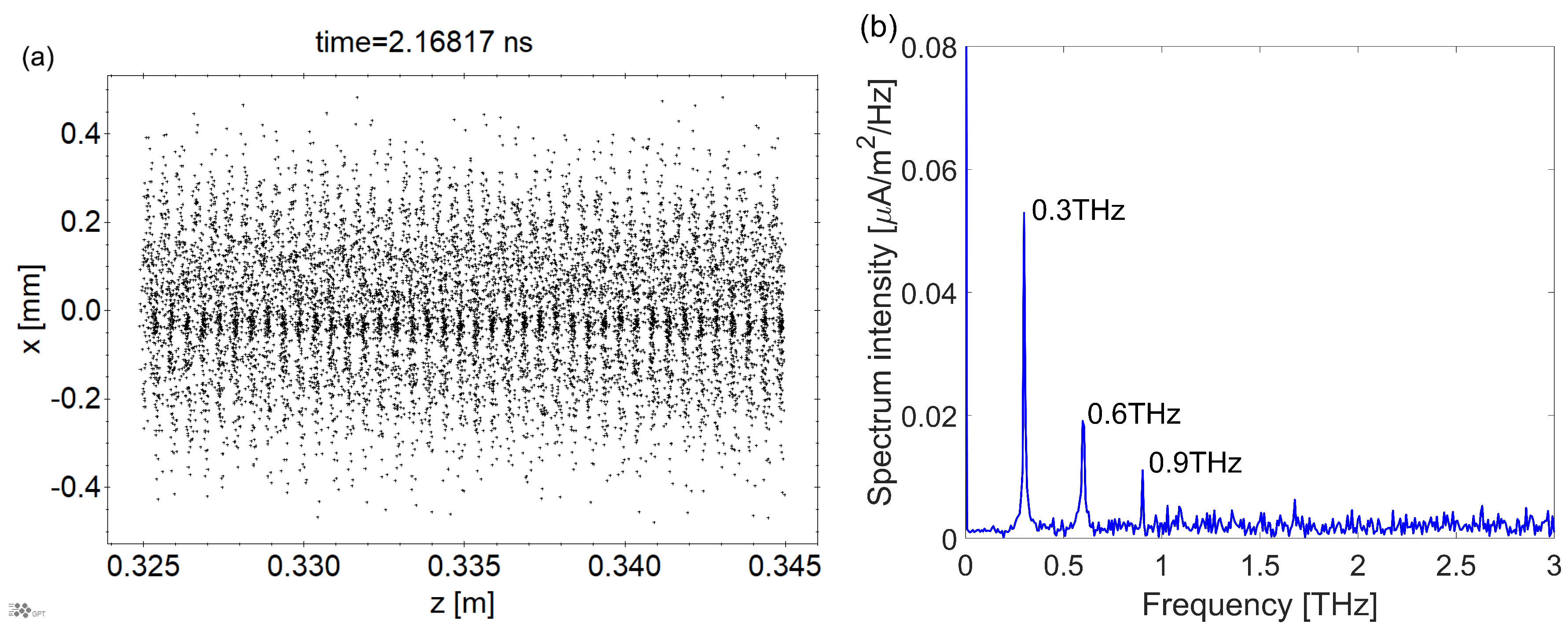
The simulation started when the head of the beam bunch entered the structure at z = 20 mm and saw the EM field. The particle distribution on the x-z plane at the time of 2.168 ns, when the tail of the bunch had passed over 300 periods of the grating, is presented in Figure 4. It is obvious that there is a significant micro-bunching pattern near the axis at x = 0. The bunching period in the z-direction was measured to be 0.5 mm, which is consistent with the previous analysis.
By counting the number of electrons in Figure 4 at a regular interval (= m) along the z-axis, we can get the statistical histogram of the number of electrons. Further, by converting the position coordinates of the horizontal axis into the time at which the particles pass the fixed point and multiplying the electron quantity by electron charge and velocity, we finally get the current intensity distribution of the macro beam bunch as shown in Figure 5a. Without loss of generality, the fixed point is designated as the bunch head’s position on the z-axis in this article. And by performing a Fourier transform on the data in Figure 5a, we can obtain its frequency spectrum, which is shown in Figure 5b. Based on Figure 5, the micro-bunching feature is more clearly revealed. Each micro-bunch has almost the same amount of charge. Nevertheless, there are still a massive number of electrons evenly distributed in the entire beam, which contributed to the considerable direct current component as shown in Figure 5b. From Figure 5b, we can also see that the micro-bunching of the electron beam is dominant by 0.3 THz and its second harmonic component.
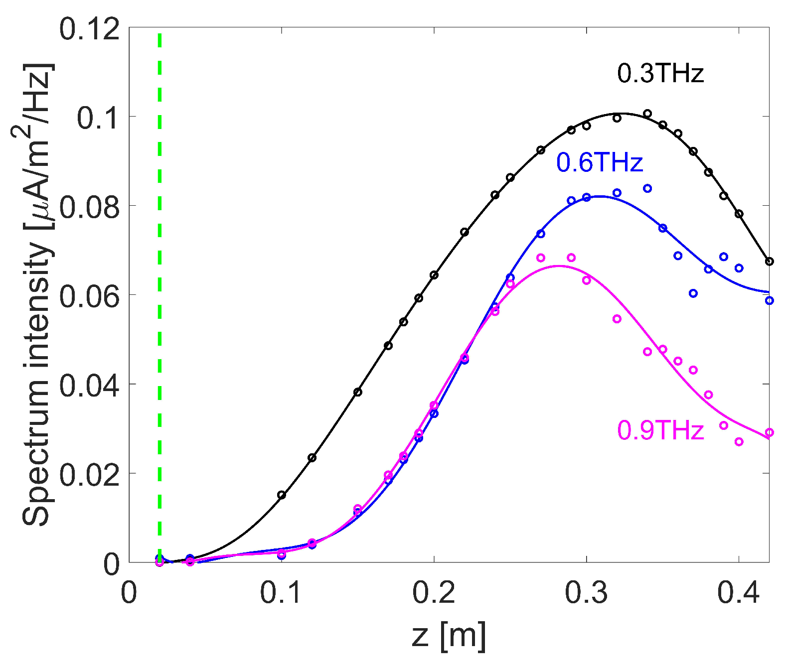
We have also observed the evolution trend of the spectrum intensities of the three lowest harmonics along the z-axis. From Figure 6, we know that the spectrum intensities of the three lowest harmonics increase steadily before reaching their top value at around z = 0.32 m, where the tail of the macro beam bunch has just passed through 300 periods of the dielectric grating. Then the spectrum intensities start to fall. By analysing the current intensity distribution graph at each time, we found that the micro-bunched electron beam began to diffuse after reaching the highest bunching level as a result of the increase in repulsive force from the space charge. So for the proposed model, it is enough to set the total number of grating periods to be 300 or less.
Next, we would like to consider the case that the electron beam has a small energy spread (0.1%) and transverse emittance ( m·rad ). In Figure 7a, one can see that the bunching effect is not so good as that shown in Figure 4. And in Figure 7b, the spectrum intensities are also lower than the result in Figure 5b). More specifically, the spectrum intensities of the three lowest harmonics are reduced to about 1/2, 1/4 and 1/4 of the corresponding values in Figure 5b. Nonetheless, the proposed model is also proven to be effective when a small energy spread and transverse emittance are considered.
4. Discussion
Considering the low energy of the electrons, the strong space charge effect is a key factor that will affect the performance of the proposed model. We studied the spectrum intensities of the three lowest harmonics under different beam charges, as shown in Figure 8a. Here we have considered a small energy spread (0.1%) and transverse emittance ( m·rad). And the electric field intensity of the incident wave was set as 1 MV/m. From Figure 8a, we can see that as the beam charge increases, the intensity of the 0.3 THz component grows remarkably, while the 0.6 THz and 0.9 THz components only see a small growth, which is due to the increase of the space charge force.
Another important factor related to the beam bunching performance is the electric field intensity of the incident plane wave. Figure 8b shows the spectrum intensities of the three lowest harmonics under different electric field intensity of the incident wave. The beam charge was set as 16 fC in the simulation. We can see that the spectrum intensities of three harmonics first increase and then decrease as the incident field increases. It can be understood that a high incident field will improve the bunching of the electron beam. Yet, if the incident field is too intense, the electrons will bunch and then disperse quickly. At the observation time, the bunches have already dispersed, which reduces the effective bunching factors.
5. Conclusions
We proposed a THz-wave-driven dual dielectric grating structure, with the aim of producing electron bunches with THz-scale repetition frequency. Structure parameters, electron energy and the incident wave’s wavelength in the proposed model were specially designed to make the electron beam bunches at the driving-wave’s frequency or its higher harmonics. According to the simulation result, the micro-bunching of the electron beam is mainly dominant by 0.3 THz and its second harmonic component. The results verified the effectivity of the proposed model, for the cases with and without energy spread and transverse emittance.
Author Contributions
Conceptualization, W.L.; investigation, L.L.; writing—original draft preparation, L.L.; writing—review and editing, W.L and L.L.; visualization, L.L.; supervision, Q.J. and Y.L.; funding acquisition, W.L., Q.J. and Y.L.
Funding
This research is supported by National Natural Science Foundation of China (Grants No. 61471332, No. 51627901, No. 11675178, and No. U1632150) and Chinese Universities Scientific Fund (Grant No. WK2310000059).
Conflicts of Interest
The authors declare no conflict of interest.
References
- Peralta, E.A.; Soong, K.; England, R.J.; Colby, E.R.; Wu, Z.; Montazeri, B.; McGuinness, C.; McNeur, J.; Leedle, K.J.; Walz, D.; et al. Demonstration of electron acceleration in a laser-driven dielectric microstructure. Nature 2013, 503, 91–94. [Google Scholar] [CrossRef] [PubMed]
- Huang, Y.C.; Zheng, D.; Tulloch, W.M.; Byer, R.L. Proposed structure for a crossed-laser beam, GeV per meter gradient, vacuum electron linear accelerator. Appl. Phys. Lett. 1998, 68, 753–755. [Google Scholar] [CrossRef]
- Lin, X.E. Photonic band gap fiber accelerator. Phys. Rev. ST Accel. Beams 2001, 4, 051301. [Google Scholar] [CrossRef]
- Lenzner, M.; Krüger, J.; Sartania, S.; Cheng, Z.; Spielmann, C.; Mourou, G.; Kautek, W.; Krausz, F. Femtosecond Optical Breakdown in Dielectrics. Phys. Rev. ST Accel. Beams 1998, 80, 4076. [Google Scholar] [CrossRef]
- Stuart, B.C.; Feit, M.D.; Rubenchik, A.M.; Shore, B.W.; Perry, M.D. Laser-Induced Damage in Dielectrics with Nanosecond to Subpicosecond Pulses. Phys. Rev. ST Accel. Beams 1995, 74, 2248. [Google Scholar] [CrossRef] [PubMed]
- Plettner, T. Phase-synchronicity conditions from pulse-front tilted laser beams on one-dimensional periodic structures and proposed laser-driven deflection. In SLAC-PUB-12458; SLAC National Accelerator Laboratory: Menlo Park, CA, USA, 2007. [Google Scholar]
- Plettner, T.; Byer, R.L. Proposed dielectric-based microstructure laser-driven undulator. Phys. Rev. ST Accel. Beams 2008, 11, 030704. [Google Scholar] [CrossRef]
- Gray, P.R.; Hurst, P.J.; Lewis, S.H.; Meyer, R.G. Analysis and Design of Analog Integrated Circuits, 5th ed.; Wiley: New York, NY, USA, 2009; p. 156. ISBN 978-0-470-24599-6. [Google Scholar]
- Plettner, T.; Lu, P.P.; Byer, R.L. Proposed few-optical cycle laser-driven particle accelerator structure. Phys. Rev. ST Accel. Beams 2006, 9, 111301. [Google Scholar] [CrossRef]
- ANSYS HFSS (High Frequency Structure Simulator). ANSYS. Available online: https://www.ansys.com/products/electronics/ansys-hfss (accessed on 1 October 2018).
- General Particle Tracer (GPT). Pulsar Physics. Available online: http://www.pulsar.nl/ (accessed on 1 October 2018).
Figure 1.
Side view (a) and front view (b) of a section of the proposed structure.

Figure 2.
(a) Contour map of the electric field’s x-direction component (phase = 0 degree) in the y-z plane. (b) The electric field’s x-direction component along the line which passes through the center of the structure. The four lines represent different initial phases of the incident wave.
Figure 2.
(a) Contour map of the electric field’s x-direction component (phase = 0 degree) in the y-z plane. (b) The electric field’s x-direction component along the line which passes through the center of the structure. The four lines represent different initial phases of the incident wave.

Figure 3.
The value of the maximum deflection electric field at the center of one grating period when phase = 0 degree (as shown in Figure 2a).
Figure 3.
The value of the maximum deflection electric field at the center of one grating period when phase = 0 degree (as shown in Figure 2a).

Figure 4.
Particle distribution on the x-z plane when time = 2.168 ns.

Figure 5.
The macro beam bunch’s current intensity distribution (a) and its frequency spectrum (b).

Figure 6.
The evolution trend of the spectrum intensities of the three lowest harmonics along the z-axis. Circle marks and lines represent measured data and their fitted curves, respectively. The green dashed line indicates the starting position of the electromagnetic field.
Figure 6.
The evolution trend of the spectrum intensities of the three lowest harmonics along the z-axis. Circle marks and lines represent measured data and their fitted curves, respectively. The green dashed line indicates the starting position of the electromagnetic field.

Figure 7.
(a) Particle distribution on the x-z plane at time = 2.168 ns when energy spread and tranverse emittance are included. (b) The corresponding frequency spectrum of the beam current.
Figure 7.
(a) Particle distribution on the x-z plane at time = 2.168 ns when energy spread and tranverse emittance are included. (b) The corresponding frequency spectrum of the beam current.

Figure 8.
The spectrum intensities of the three lowest harmonics under (a) different initial beam charges and (b) different eletric field intensities of the incident plane wave.
Figure 8.
The spectrum intensities of the three lowest harmonics under (a) different initial beam charges and (b) different eletric field intensities of the incident plane wave.


Table 1.
Proposed model parameters.
| Parameter Names | Symbols | Values |
|---|---|---|
| Electron beam parameters | ||
| Electron energy | 79 keV | |
| Bunch length | 20 mm | |
| Transverse radius | 0.01 mm | |
| Driving wave and grating parameters | ||
| Driving wave’s wavelength | 1 mm | |
| Grating length | L | 1 mm |
| Number of periods | 400 | |
| Grating pillar height | h | 0.5 mm |
| Grating pillar width | d | 0.6 mm |
| Channel gap width | g | 0.5 mm |
| Structure transverse width in x-direction | w | 4 mm |
| Base plate thickness | b | 0.5 mm |
© 2018 by the authors. Licensee MDPI, Basel, Switzerland. This article is an open access article distributed under the terms and conditions of the Creative Commons Attribution (CC BY) license (http://creativecommons.org/licenses/by/4.0/).
Share and Cite
MDPI and ACS Style
Liang, L.; Liu, W.; Jia, Q.; Lu, Y. Generation of THz Modulated Electron Bunches Using Transversally Polarized Waves to Drive a Dielectric Dual-Grating. Particles 2018, 1, 253-259. https://doi.org/10.3390/particles1010019
AMA Style
Liang L, Liu W, Jia Q, Lu Y. Generation of THz Modulated Electron Bunches Using Transversally Polarized Waves to Drive a Dielectric Dual-Grating. Particles. 2018; 1(1):253-259. https://doi.org/10.3390/particles1010019
Chicago/Turabian StyleLiang, Linbo, Weihao Liu, Qika Jia, and Yalin Lu. 2018. "Generation of THz Modulated Electron Bunches Using Transversally Polarized Waves to Drive a Dielectric Dual-Grating" Particles 1, no. 1: 253-259. https://doi.org/10.3390/particles1010019