Primary Design of Extended Interaction Klystron with Multi-Gap Cavity at 225 GHz


THz Research Center, School of Electronic Science and Engineering, University of Electronic Science and Technology of China, Chengdu 610054, Sichuan, China
*
Author to whom correspondence should be addressed.
Particles 2018, 1(1), 260-266; https://doi.org/10.3390/particles1010020
Submission received: 16 October 2018
/
Revised: 7 November 2018
/
Accepted: 8 November 2018
/
Published: 11 November 2018
(This article belongs to the Special Issue Superradiances from Ultra Short Electron Bunch Beam)
Abstract
:The analytical expressions of the beam–wave coupling coefficients and the beam loading conductance for a 2π mode in a multi-gap cavity is proposed as a circuit of the extended interaction klystron (EIK), are derived by space-charge wave theory. The mechanism of the beam–wave synchronization and the coupling in the multi-gap cavity at 225 GHz are studied in detail by calculating the coupling coefficient and the normalized beam loading conductance as a function of gap number, gap dimension, and beam voltage as well as the perveance. The stability of the circuit is analyzed by considering the quality factor of the electron beam. It is found that the stability of the operating 2π mode is more sensitive to the beam voltage and gap number. Based on the theory and analysis, a 5-gap coupled cavity is proposed as a section of EIK’s circuit. A low voltage EIK with a 4-cavity circuit at 225 GHz is designed and is simulated by a particle-in-cell (PIC) code. The EIK can achieve a maximum output power of ~36 W with more than 30 dB gain at 225 GHz.
1. Introduction
The vacuum tube is a versatile type of terahertz (THz) device [1,2,3] that has been found in many applications such as space communications, deep space technology, modern radar, climate observation imaging [4,5,6,7]. The extended interaction klystron (EIK) [4,5], based on the extended interaction structure, is the preferable choice of a vacuum tube for high power operation, low voltage and compact size, especially in the millimeter, submillimeter, and THz wave band [5]. CPI’s EIK device can achieve 50 W for pulsed and 10 W for CW at 220 GHz. The EIK is a combination of the klystron and the traveling wave tube technology, which has a cavity that consists of multiple gaps instead of a single gap like in the ordinary klystron resonator. The cavity that consists of multiple gaps can increase the interaction impedance when the electron velocity is synchronized with the gap electric fields, and this is the key to EIK’s higher power gain and efficiency at the millimeter and THz band. Due to the multiple gaps, the electric field intensity in each gap can be reduced significantly to avoid the breakdown, and thus to improve the peak power. Therefore, the EIK can realize short interaction circuit, compact size, and low voltage at millimeter band and THz band.
The space charge wave theory [8,9] was used to analyze the beam–wave interaction in a single-gap cavity. However the space charge wave theory is seldom investigated for multi-gap cavity. Thus, in this paper, we shall study the beam–wave coupling in a multi-gap cavity based on this theory to analyze how the gap size, gap number, and the beam voltage influence the beam–wave synchronization and the beam–wave coupling. Then, the stability of the operating mode in multiple gaps for different numbers of gaps is analyzed by its quality factor. Furthermore, a coupled cavity with multi-gap structure is presented as the circuit for an EIK operating at 225 GHz at low voltages.
2. Beam–wave Interaction in Multi-Gap Cavity
The general derivation of small signal beam loading conductance Gb with space charge is given by [8]
where βe and βp are the electron wavenumber and electron plasma wavenumber, respectively. Here, Ms and Mf refer to the beam coupling coefficient for the fast wave (βe − βp) and the slow wave (βe + βp) component of the space charge wave of the beam, respectively, and are expressed as
where the function of f (z) is the distribution of the E-field.
EIK usually operates at π mode or 2π mode. Assuming a 2π mode, its longitudinal RF standing electric field has a periodic distribution and is a constant in the gaps. For a cavity consisting of N gaps, the electric field on the ith gap is expressed as
where d and L is the length of the gap and of the period, respectively. By substituting Equation (3) to Equation (2), we have
In Equation (4) the first term is the coupling coefficient for the single gap, and the second term includes the influence of gap number N and gap size, as well as the beam voltage. From Equaiton (1), we define a normalized beam loading conductance:
where G0 = I0/V0 is the DC beam conductance. The power transferred can be judged between the circuit and the beam according ge with positive or negative value.
Under the condition of L = 0.27 mm, d = 0.12 mm, and the voltage 11 kV, as well as f = 225 GHz, the beam–wave coupling coefficient M2 and the normalized beam loading conductance ge are plotted in Figure 1 as a function of gap number N and the velocity parameter ε = 1 − vp/v0 at f = 225 GHz, where vp is the 2π synchronism phase velocity, and v0 is the beam velocity. The parameter ε indicates the degree of beam velocity deviates from the phase synchronism velocity. The coupling is the strongest near to the synchronism condition ε = 0 in Figure 1a, as expected. At higher N, Figure 1 shows that, M2 and ge vary more rapidly with beam voltage. It indicates that the gap number can improve the beam–wave interaction in some extent. The coupling is the strongest near to the synchronism condition.
When the beam velocity is lower than synchronous velocity (ε < 0), the coupling occurs between the circuit mode and the fast space-charge wave, and the power is mainly transferred from the circuit to the beam, which gives ge > 0. While ge < 0 corresponds to the case ε > 0. Thus ge exists two extreme points (positive and negative). If the negative beam loading is sufficiently high to compensate the losses in the cavity, the energy will be transferred from the beam into an electromagnetic wave. This requires that the operating voltage is little higher than synchronism one.
According to Equation (4), the gap size influences the coupling. Assuming a fixed voltage of 11 kV, the calculated M2 and ge as a function of βeL/π is shown in Figure 2a for L from 0.20 to 0.36 mm, corresponding to βeL/π from 1.4 to 2.6. For a fixed period of 0.27 mm, the corresponding M2 and ge as a function of βeL/π from 1.6 to 2.3, for V from 17 to 8 kV, is shown in Figure 2b. It is clear that M2 still reaches the maximum near the 2π point. When L is shorter or when V is larger than that of the synchronism condition, ge reaches the minimum. This means that a slightly smaller period or a slightly larger voltage can enhance the beam–wave interaction and improve the beam–wave coupling efficiency.
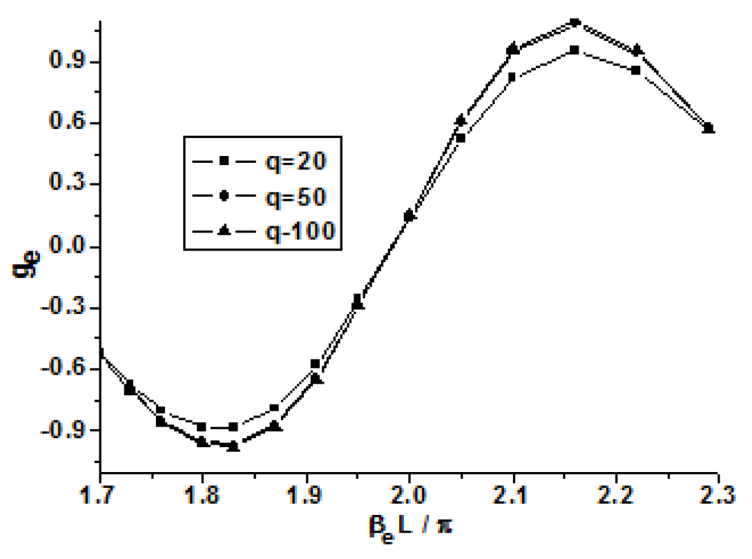
To analyze the influence of the perveance to the beam–wave interaction, we define q = βe/βp as the space charge factor. For example, q = 20, 50, 100 corresponds to a current density of approximately 1500, 240, 60 A/cm2, respectively. In Figure 3 we show the dependence of ge as a function of βeL/π at 11 kV with L from 0.23 to 0.33 mm. It clearly indicates that the space charge effect at higher perveance (or smaller q) will reduce ge and beam–wave interaction.
Beam loading conductance is usually used to represent the magnitude of interaction between the electron beam and the electric field in the gap. However, the interaction may cause instability in the cavity for larger negative ge with larger gap number. To analyze the stability condition, we define the quality factor of electron beam, Qb. In Figure 4, the dependence of Qb on voltage for various gap number, N from 4 to 7, is shown. A sharp step occurs from positive to negative values for Qb near the synchronism condition at approximately 10.5 kV to 11 kV. When the voltage is higher than 11 kV, the magnitude of Qb sharply increases with the gap number N, which is partly due to the magnitude of ge and the value of R/Q both increasing with N (as shown in Figure 5b). This will cause unstable operation for larger gaps number. For the gap number N from 4 to 5, the value of −Qb is relatively constant in the voltage range 12 kV to 13 kV in Figure 4, indicating that the operation is stable.
3. Cold and Hot Simulation
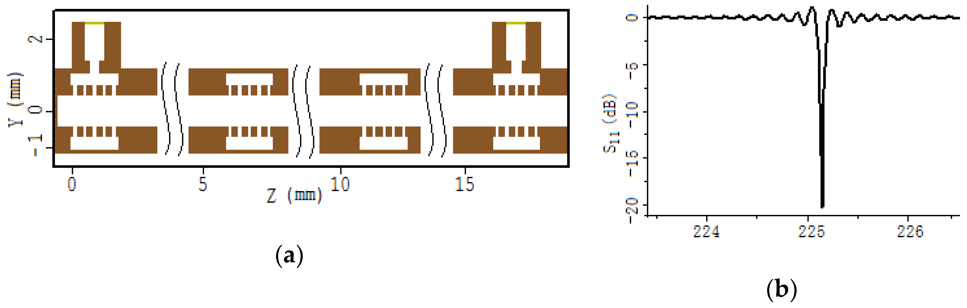
In this section, we design a low voltage EIK device operating at 225 GHz, based on the results obtained from Sec. II. A coupled cavity is adopted as the circuit of the EIK device. According the results from Figure 1, Figure 2, Figure 3 and Figure 4, a 5-gap coupled cavity is used, with the gap dimensions of L = 0.27 mm and d = 0.12 mm, in the section of the circuit illustrated in Figure 5a. The value of R/Q at three different locations (axial line, edge of beam tunnel, and edge of gap) in the cavity is calculated, with the gap number N from 2 to 8 for the 2π mode shown in Figure 5b.
The results show that R/Q increases linearly with N, and stronger beam–wave interaction will occur at the region near to the edge of beam tunnel. When gap number is equal to 5, the value of R/Q can reach 77 Ω, 95 Ω, and 130 Ω at the three locations, respectively. It is clear that the multi-gap coupled cavity, which has simple geometry and high impedance, can support efficient beam–wave interaction and energy exchange between the RF field and electron beam.
As far as the circuit is concerned, the EIK device has several multi-gap cavities. A circuit consisting of four cavities is designed as shown in Figure 6a, with a circuit length of about 19 mm. The input cavity is very important because it must allow the input of sufficient electromagnetic energy. The S11 parameter of the input cavity for a 2π mode is shown in Figure 6b. The peak frequency is at around 225.2 GHz and its corresponding S11 value is below −20 dB, which means most of the energy from the 2π mode can be injected into the input cavity to support energy exchange between and electron beam and the RF field. However, the band is not broad enough. Nevertheless, we focus more on the beam–wave interaction and put less emphasis on the band.
A specialized particle-in-cell (PIC) code [10] is used to simulate the beam–wave interaction in the EIK device under a current density of 80 A/cm2 (about 100 mA) and a beam voltage of 13 kV, as well as a longitudinal homogeneous magnetic field of 0.5 T. Based on the multi-cavity klystron, the transition angles of the drift are from 80° to 90°, 45° to 60°, and 30° to 45° in the linear, bunching, and output section, respectively. The output power at frequency of 224.65 GHz and varying with the input power is shown as Figure 7a. The output power is up to 30 W with a 30 dB gain. The reason the curve in Figure 7a first rises and then falls is due to the beam–wave interaction and beam modulation increasing with the input power. The interaction breaks down due to higher input power leading to overmodulation. Furthermore, the output power with the beam voltage is investigated as shown in Figure 7b. When the beam voltage is near to the synchronous condition, the power can reach the maximum value. For beam voltage lower or higher than the synchronous voltage, the power is lower.
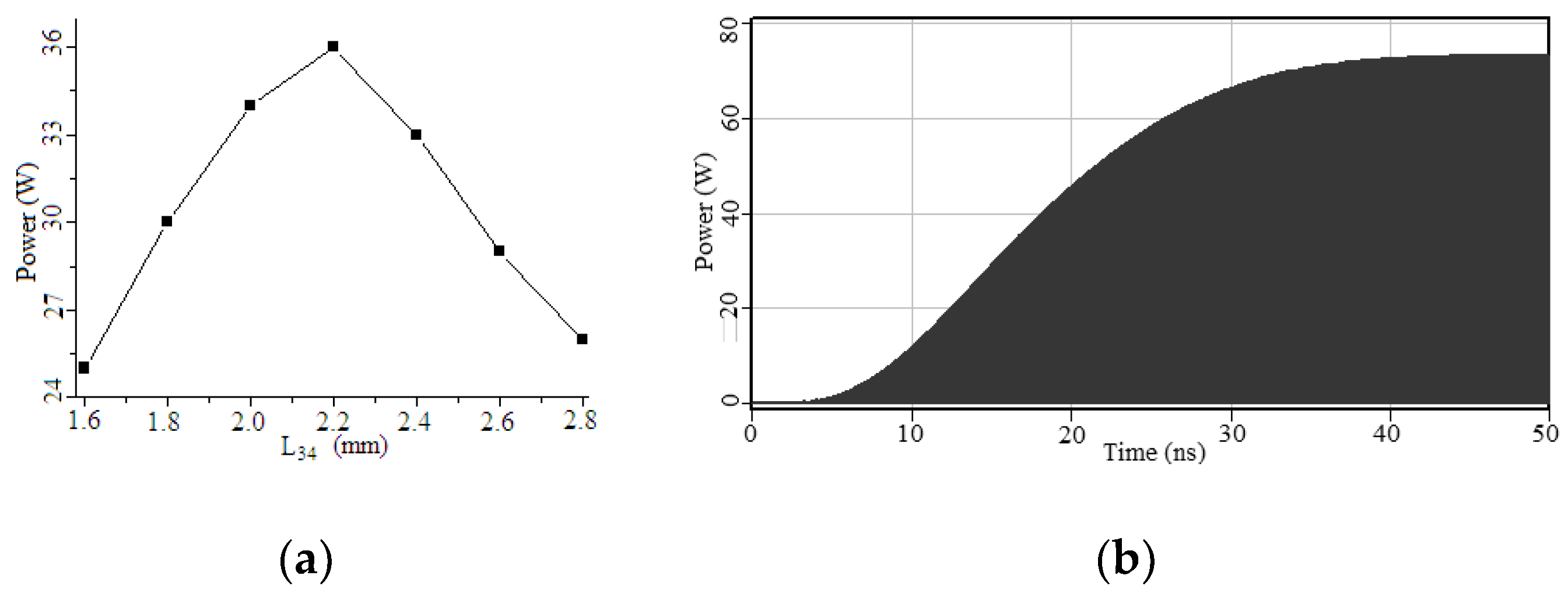
The length of the drift tube can influence the beam bunching and the interaction efficiency. The length of the drift tube L34 (between the 3rd and 4th cavity) is optimized, with the simulation results shown as Figure 8. The output power first increases with L34 and then decreases after exceeding 2.2mm, owing to the beam debunching. The maximum power can reach 36 W with an efficiency of approximately 2.8% and a gain of 30.8 dB. Its spectrum varies with time as shown in Figure 8b. With a short multi-gap coupled cavity, the EIK device can provide high power and high gain per length to ensure stable operation at low and reasonable operating voltages and at submillimeter and THz band frequencies. The output power can reach the level of CPI’s EIK device [5].
4. Conclusions
Based on the space charge wave theory, the coupling coefficient and the beam loading conductance for a 2π mode for extended interaction klystron (EIK) are formulated in this paper. The coupling coefficient and the beam loading conductance, as a function of gap numbers, space charge factor and perveance are calculated at 225 GHz. The stability of the circuit is analyzed by calculating the quality factor of the electron beam. It is found that the stability of the 2π mode is more sensitive to the voltage for large gap numbers. A coupled cavity consisting of a multi-gap structure is proposed as the circuit for an EIK device operating at low voltages. The EIK’s characteristic is analyzed as a function of the voltage, input power and drift length. The maximum output power is up to 36 W with a gain of more than 30 dB and efficiency of 2.8% at 224.65 GHz. Results indicate that a short interaction circuit in the EIK provides high gain per length, with the use of a single permanent magnet to focus the electron beam and a relatively light package for compact size. Therefore, this EIK is compact, uses low voltage and has high efficiency, which is suitable for use as sub-mm transmitter or sub-mm radar, and has the potential to be a THz high power source. However, the bandwidth is not broad, thus the next study would be to improve the bandwidth and to develop the primary experiment.
Author Contributions
Conceptualization, K.Z.; Methodology, K.Z. and K.C.; Software, K.C. and Q.X.; Validation, X.C.; Formal Analysis, W.X. and N.X.; Investigation, W.X. and N.X.; Resources, X.C.; Data Curation, K.C. and Q.X.; Writing—original draft preparation, K.Z.; Writing—review and editing, K.Z.; Project Administration, K.Z.; Funding Acquisition, D.L.
Funding
This research was funded by the National Key Research and Development Program of China, grant number 2017YFA0701000).
Acknowledgments
The authors acknowledge PhD Kelvin Ooi Jian Aun in Xiamen University Malaysia for his English checking.
Conflicts of Interest
The authors declare no conflict of interest.
References
- Hou, Y.; Gong, Y.B.; Xu, J.; Wang, S.M.; Wei, Y.Y.; Yue, L.N.; Feng, J.J. A Novel Ridge-Vane-Loaded Folded-Waveguide Slow-Wave Structure for 0.22-THz Traveling-Wave Tube. IEEE Trans. Electron Devices 2013, 60, 1228–1235. [Google Scholar] [CrossRef]
- Cai, J.; Wu, X.P.; Feng, J.J. Traveling-Wave Tube Harmonic Amplifier in Terahertz and Experimental Demonstration. IEEE Trans. Electron Devices 2015, 62, 648–651. [Google Scholar] [CrossRef]
- Shu, G.X.; Liu, G.; Qian, Z.F. Simulation study of a high-order mode terahertz radiation source based on an orthogonal grating waveguide and multiple sheet electron beams. Optics Express 2018, 26, 8040–8048. [Google Scholar] [CrossRef] [PubMed]
- Roitman, A.; Berry, D.; Steer, B. State-of-the-art W-band extended interaction klystron for the CloudSat program. IEEE Trans. Electron Devices 2005, 52, 895–898. [Google Scholar] [CrossRef]
- Roitman, A.; Berry, D.; Hyttinen, M.; Steer, B. Sub-Millimeter Waves from a compact, low voltage Extended Interaction Klystron. In Proceedings of the 2007 Joint 32nd International Conference on Infrared and Millimeter Waves and the 15th International Conference on Terahertz Electronics, Cardiff, UK, 2–9 September 2007; pp. 1–3. [Google Scholar] [CrossRef]
- Zhang, K.C.; Wu, Z.H.; Yan, Y.; Huang, Y.; Li, X.Y.; Liu, S.G. Design and Preliminary Experiment of 35 GHz Pulsed Extended Interaction Oscillator with Folded Waveguide. J. Infrared Millim. Terahertz Waves 2010, 31, 543–550. [Google Scholar] [CrossRef]
- Yin, Y.; He, W.L.; Zhang, L.; Yin, H.; Cross, A.W. Preliminary design and optimization of a G-band extended interaction oscillator based on a pseudospark-sourced electron beam. Phys. Plasmas 2015, 22. [Google Scholar] [CrossRef] [Green Version]
- Preist, D.H.; Leidigh, W.J. Experiments with high-power CW klystrons using extended interaction catchers. IEEE Trans. Electron Devices 1963, 10, 201–211. [Google Scholar] [CrossRef]
- Zhang, K.C.; Wu, Z.H.; Liu, S.G. Study of An Extended Interaction Oscillator with a Rectangular Reentrance Coupled-cavity in Terahertz Region. J. Infrared Millim. Terahertz Waves 2009, 30, 309–318. [Google Scholar] [CrossRef]
- Zhou, J.; Liu, D.G.; Liao, C.; Li, Z.H. CHIPIC: An Efficient Code for Electromagnetic PIC Modeling and Simulation. IEEE Trans. Plasma Sci. 2009, 37, 2002–2011. [Google Scholar] [CrossRef]
Figure 1.
M2 and ge vary with N and ε, (a) M2 and, (b) ge.

Figure 2.
M2 and ge vary with (a) period L and, (b) voltage V.

Figure 3.
M2 and ge vary with perveance.

Figure 4.
Qb with voltage and gaps number.

Figure 5.
Schematic of the cavity (a) and R/Q plotted with gap number (b).

Figure 6.
Circuit of the extended interaction klystron (EIK) (a) and the S11 parameter of the input cavity (b).
Figure 6.
Circuit of the extended interaction klystron (EIK) (a) and the S11 parameter of the input cavity (b).

Figure 7.
PIC simulation results: (a) output power vs. input power and (b) output power vs. voltage.
Figure 7.
PIC simulation results: (a) output power vs. input power and (b) output power vs. voltage.

Figure 8.
Optimal output power vs. length of drift tube L34 (a) and vs. time (b).

© 2018 by the author. Licensee MDPI, Basel, Switzerland. This article is an open access article distributed under the terms and conditions of the Creative Commons Attribution (CC BY) license (http://creativecommons.org/licenses/by/4.0/).
Share and Cite
MDPI and ACS Style
Zhang, K.; Chen, K.; Xu, Q.; Xu, W.; Xiong, N.; Chen, X.; Liu, D. Primary Design of Extended Interaction Klystron with Multi-Gap Cavity at 225 GHz. Particles 2018, 1, 260-266. https://doi.org/10.3390/particles1010020
AMA Style
Zhang K, Chen K, Xu Q, Xu W, Xiong N, Chen X, Liu D. Primary Design of Extended Interaction Klystron with Multi-Gap Cavity at 225 GHz. Particles. 2018; 1(1):260-266. https://doi.org/10.3390/particles1010020
Chicago/Turabian StyleZhang, Kaichun, Ke Chen, Qian Xu, Wangju Xu, Neng Xiong, Xiaoxing Chen, and Diwei Liu. 2018. "Primary Design of Extended Interaction Klystron with Multi-Gap Cavity at 225 GHz" Particles 1, no. 1: 260-266. https://doi.org/10.3390/particles1010020