
Surface Functionalization of TiO2 Nanotubes Modified with a Thin Film of BiFeO3


1
Amirkhanov Institute of Physics, Dagestan Federal Research Center, Russian Academy of Sciences, 367003 Makhachkala, Russia
2
Smart Materials Laboratory, Department of Inorganic Chemistry and Chemical Ecology, Dagestan State University, 367015 Makhachkala, Russia
*
Author to whom correspondence should be addressed.
Surfaces 2024, 7(1), 1-11; https://doi.org/10.3390/surfaces7010001
Submission received: 19 October 2023
/
Revised: 14 December 2023
/
Accepted: 15 December 2023
/
Published: 19 December 2023
Abstract
:The atomic layer deposition method allows for the production of a thin film with a high aspect ratio on the uneven surface of titanium dioxide nanotubes TiO2(Nt). A modified BiFeO3/TiO2(Nt)/Ti (BFOT) structure with controllable electrical characteristics was obtained. BFOT possesses both ferroelectric and semiconductor properties with nonlinear conductivity dependent on the magnitude and duration of the voltage supply. Analysis of the temperature dependence of charge variation showed leakage currents in the BFOT structure due to the capture and release of charge carriers from defect levels. Surface modification of nanotubes with the multiferroic BiFeO3 allows for the creation of semiconductors with adaptive functional properties.
1. Introduction
Improving materials for resistive switching devices and field-effect transistors based on ferroelectrics is closely related to optimizing the surfaces of these materials [1,2,3,4,5]. There is growing interest in combining these elements as field-effect transistors based on TiO2 memristors with a programmable set/reset for neuromorphic computing [6]. Adding functionality to control the characteristics of memristive structures is a promising strategy for improving such devices. From the perspective of memory universality, it should have an unlimited number of write/read cycles and low power consumption and cost, and provide high information density and the potential for further scaling [7,8]. Ferroelectric (FeRAM) and resistive (ReRAM) memory are considered promising candidates for creating next-generation memory devices that meet the above requirements. From this point of view, the multiferroic BiFeO3 (BFO), which combines the magnetoelectric effect and the resistive switching effect (RS) at low voltage values, has recently attracted great interest [9]. Thin BFO films, both epitaxial and polycrystalline, due to their excellent properties [10,11], such as residual polarization Pr, reverse piezoelectric effect, and high Curie temperature TC = 820–850 °C, are promising materials for resistive switching devices.
It has been noted that structures based on BFO have high leakage currents [12]. A reduction in leakage currents can be achieved through various methods, including creating interfaces with other materials [12]. Another way is through doping BFO with Mn [13], or Co and Ti [14]. Doping with titanium reduces leakage currents, but destroys the piezoelectric properties as it is impossible to achieve coercive field strength. Leakage currents are considered undesirable in thin film ferroelectrics when used in memory devices. However, controlling leakage currents is a key feature that plays a role in the memory process in memristive structures [15]. Creating structures with the ability to control leakage currents and electrical polarization can be interesting for the field of creating field-effect transistors based on ferroelectrics and in applications using artificial synapses that approximate natural analogs. Titanium oxide can be considered a model material for resistive switching devices [16]. Phase transformations in TiO2 can create various conductivity regions, including biased conductivity [17].
ALD technology allows for the production of functional layers on surfaces, including polymers [18]. The thinness of the layers allows for a reduction in their crack resistance [19]. Reconfigurable flexoelectricity, caused by bending a flexible substrate, induces non-uniform distortion of the BFO lattice, affecting the inversion asymmetry of the film [20]. Thus, multi-level conductivity is achieved through the connection between the flexoelectric and ferroelectric properties of the film [21]. The multi-level conductivity of the BFOT structure enables its use as an analog memristive structure [22].
Using two oxides with different ion potentials can induce a positive surface charge and reduce the work function of the original material with mixed conductivity. Surface dipoles in ferroelectrics caused by changes in the energy landscape can redistribute electron charge densities. Charge redistribution, in turn, can contribute to geometric surface reorientation.
2. Materials and Methods
BFO films were grown using a sequentially pulsed chemical vapour deposition method on a titanium plate substrate, which had previously been coated with a TiO2(Nt) film in the form of vertical nanotubes using an electrochemical method. In the absence of the use of quartz microbalances, the adopted method cannot be demonstrated to be strictly an atomic layer deposition (ALD) one, but for the sake of simplicity, we will use the acronym ALD in the following. This method enables the growth of films with 100% conformity, which is important for the chosen system. The thickness of the TiO2(Nt) layer was approximately 2.5 μm. Tris(1-methoxy-2-methyl-2-propoxy) bismuth) (Bi(mmp)3) and ferrocene (Fe(cp)2) were used as precursor sources. In the ALD process, precursors were delivered to the chamber using a 99.999% pure N2 carrier gas. The temperature range for Bi(mmp)3 evaporation was 135–145 °C, and the temperature for ferrocene evaporation was 90 °C. The ALD BiOx consisted of a 1.2 s precursor pulse of Bi(mmp)3, followed by a 5 s N2. Then, an O3 pulse was applied for 5 s, followed by purging of the chamber with N2 for 15 s. Then, ALD FeOx cycles were applied. The duration of the Fe(C5H5)2 precursor pulse was 2 s, and the number of subcycles for each precursor was 90. Throughout the experiment, the input and output gas lines were maintained at a temperature of 150 °C. The substrate was located 4–5 cm from the entrance. The diameter of the reactor was 20 cm. The temperature window for the Bi(mmp)3 precursor was in the range of 200–300 °C, and the saturation mass growth started at 1.0 s [23]. Using ferrocene, the optimal temperature for the self-limiting reaction with ozone was 200 °C [24]. In an earlier study, a more linear region can be identified in the temperature window of 210–260 °C, and the saturation mass growth was achieved at 2 s [25]. When producing BFO in a single technological cycle with alternating precursors, a linear growth value of the BFO film was achieved in the temperature range of 250–330 °C [26]. Based on these considerations, a growth temperature of 250 °C was chosen for this experiment.
Afterward, the obtained samples underwent thermal treatment in air at a temperature of 660 °C for 60 min. Due to the diffusion into the pores of the nanotube array, it is difficult to accurately measure the thickness of the film. The approximate thickness of the film is around 90 nm. For electrical measurements, platinum contacts were applied to the surface of the structure using magnetron sputtering, with the titanium substrate serving as the bottom electrode. Figure 1 shows the diagram of the process of layer-by-layer formation of Bi-O/Fe-O film on the surface of TiO2(Nt)/Ti substrate.
Characterization of the obtained heterostructures was performed using scanning electron microscopy (SEM) with a Magellan (Thermo Fisher Scientific, Hillsboro, OR, USA) scanning electron microscope. X-ray diffraction (XRD) studies were conducted using an Empyrean PANalytical X-ray diffractometer (Almelo, the Netherlands) in the radiation of a copper anode with a nickel filter, with radiation wavelength λ(CuKα) = 0.154051 nm. Raman spectra were examined with a Laser Raman 3D scanning confocal microscope (Ntegra Spectra, Moscow, Russia) using a green laser (532 nm) with a spot size of 1 µm and a resolution of 0.5 cm−1. The surface was examined using piezoresponse force microscopy (PFM) methods, such as variation in atomic force microscopy (AFM). Electrical measurements were performed using a Keithley 2400 source measure unit. The voltage sweep for the current–voltage (I–V) measurements was a bi-directional triangular signal (0 V → 15 V → 0 V → −15 V → 0 V). At each point of the voltage sweep, the measurement was conducted using the following scheme: voltage generation–delay (waiting)–current measurement. The delay time varied from 0.01 s to 1 s. The normal measurement speed option of the instrument was chosen. The measurement speed option was normal and corresponded to the integration time of the incoming signal 0.1 s. The sample temperature was set by a resistive heater and monitored by a type-K thermocouple.
3. Results
3.1. Structural Characteristics
The surface of the nanotubes has a large area both on the surface and on the sides where pores remain. The ALD method allows for high aspect ratio coverage of almost all open areas. Figure 2 shows the surface of the nanotubes before and after the deposition of the BFO film. As can be seen, the surface is covered with an array of vertically oriented TiO2(Nt) with a diameter of around 100–200 nm and a wall thickness of approximately 10 nm. This morphology of TiO2(Nt) allows for a significantly increased surface area compared to a titanium oxide film. Consequently, the number of active centers for interaction during the ALD process with the BFO film is also increased.
From Figure 2, it can be seen that almost the entire uneven surface of the nanotubes is covered by a film. However, there are still pores with sizes up to 60 nm after coating with the BFO film. As can be seen from the profiles, the film even penetrates inside the nanotubes, filling them from the inside.
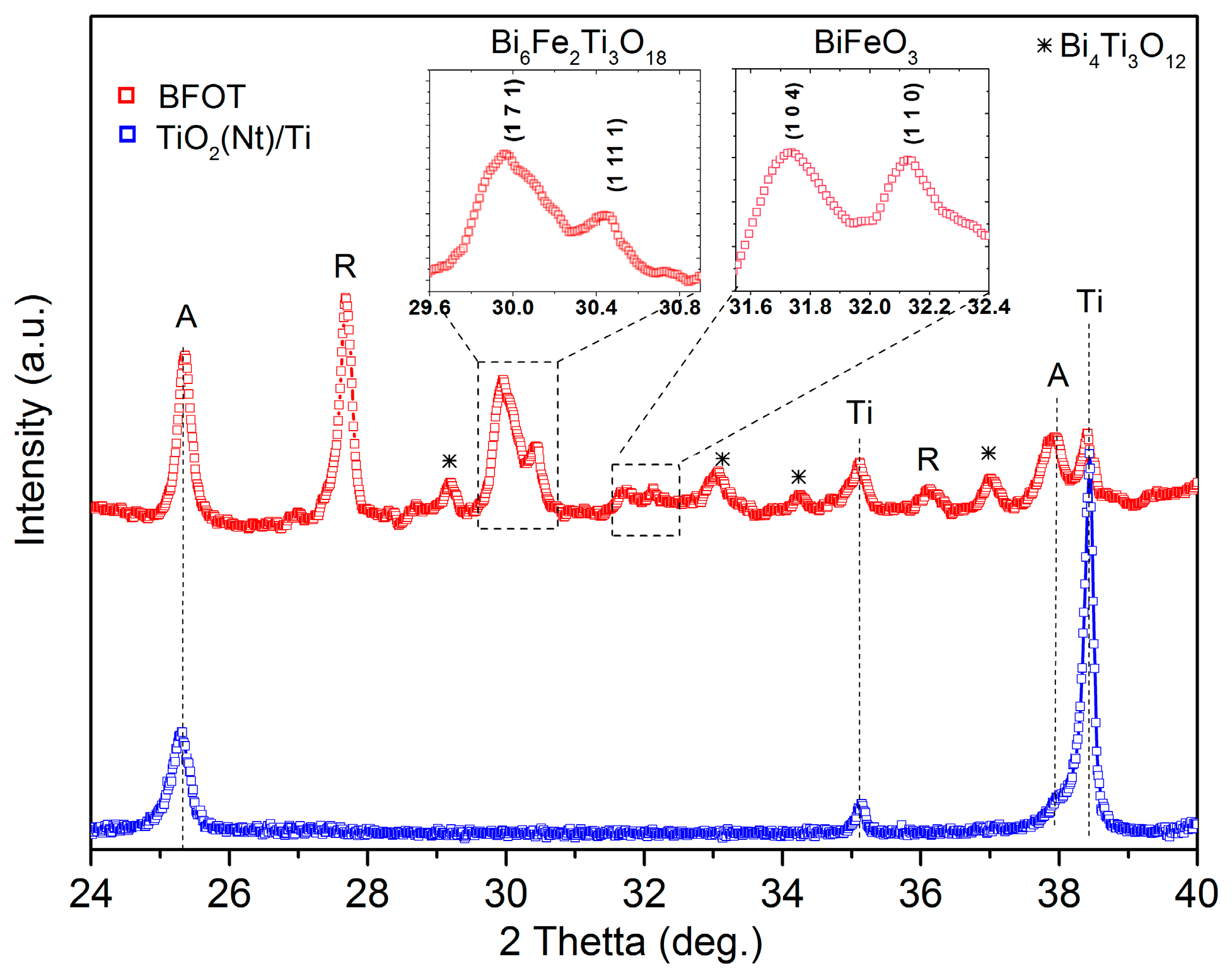
Figure 3 shows the XRD of TiO2(Nt)/Ti substrate with a nanotube array and the obtained heterostructure BFOT. As can be seen from Figure 3, many peaks overlap due to the large number of phases. During thermal treatment of the structure at the interface, a phase transformation from anatase to rutile occurs (A, R designations of peaks in Figure 3). After annealing at 660 °C, an initial phase of anatase partially transformed into the rutile phase with the characteristic diffraction peak at 2θ = 27.7° (110).
As can be seen from the XRD results in Figure 3, the peaks at 29.9°, 30.1°, 33.1°, 34.3°, and 37.2° correspond to the Bi4Ti3O12 with Aba2 space group [27]. The peaks at 31.7° (104) and 32.1° (110) are attributed to the BiFeO3 film structure with R3c space group, which is highlighted in the inset [28]. The peaks at 30.1° (171) and 30.4° (1 11 1) are related to the layered structure of Bi6Fe2Ti3O18 with Fmm2 space group [29].
Since Raman spectroscopy is sensitive to structural changes, it can provide valuable information about lattice properties and phase transitions. Figure 4 shows the Raman scattering spectra.
For comparison, the substrate spectra with an array of TiO2(Nt) nanotubes in the anatase structure are presented. In the low-frequency range of the spectra (below 200 cm−1), the characteristic modes correspond to the vibrations of Bi3+ ions in the (Bi2O2)2+ layer and the vibrations of Bi3+ ions relative to oxygen octahedra. The high-frequency modes above 200 cm−1 characterize the bending and stretching modes of the BO6 octahedra. Peaks 144 cm−1, 396 cm−1, 513 cm−1, 634 cm−1, respectively, belong to vibrations Eg, B1g, A1g, Eg the anatase TiO2 crystal lattice [30]. The newly appearing shoulders at 469 cm−1 and 612 cm−1 refer to the partially disordered of the rutile TiO2 structure [31]. The rutile phase is observed due to phase transformations at the boundary with the BFO film. In the high-frequency range above 400 cm−1, all peaks are asymmetric, and they can be interpreted as a superposition of several closely spaced modes. The mode at 340 cm−1 corresponds to the twisting vibration of Ti/FeO6 octahedra, while the modes at 567 cm−1 and 800 cm−1 are related to the stretching of octahedral chains O-Ti/Fe between (Bi2O2)2+ layers. The asymmetric peak with a mode in the range of 844 cm−1 corresponds to fully asymmetric valence vibrations of O-Ti-O and O-Fe-O bonds in Ti/FeO6 octahedra [32]. The formation of phonon modes at 567 cm−1 and 706 cm−1 is due to the combination of stretching of the Bi-Fe-O bond and octahedral bending. Peaks in the range of 221 cm−1 to 267 cm−1 correspond to the vibrations of Ti/FeO6 octahedra in BFTO. Additionally, peaks characteristic of BFO and Bi4Ti3O12 are observed. The multi-component nature of the BFTO compound formed at the film-substrate interface can change its properties in the interfacial region due to diffusion mechanisms. Dynamic phase transformations contribute to the nonlinearity of conductivity depending on the applied voltage, charge delivery time, and accumulation of defect levels.
In the BFOT structure, resistance changes occur upon the application of voltage with the formation of phase boundaries and redistribution of oxygen vacancies. The presence of Fe and Ti ions in the structure with oxidation states different from the homogeneous crystalline structure induces oxygen vacancies necessary to maintain the electronic neutrality of the system. The formation of oxygen vacancies reduces intrinsic defects, which are well-known capture centers for carrier recombination. This effect promotes electron–hole separation. The appearance of Ti3+ is caused by Fe atoms partially replacing Ti atoms in TiO6 octahedra. Similarly to the Fe3+ → Fe2+ transition, replacement upon Ti4+ → Ti3+ transition leads to an enhancement of ferroelectric residual polarization. Additionally, there is an enhancement of Bi 6s electron hybridization with 2p oxygen orbitals, which contributes to the generation and enhancement of hole mobility and shift of the valence band edge. Thus, upon the application of bias, non-uniform regions with different conductivity caused by redox processes in the material are formed.
Thermal treatment leads to a solid-phase chemical reaction in the near-surface region: 3TiO2 + 2Bi2O3 → Bi4Ti3O12. At concentrations of n(Bi)/n(Ti) > 1 in the Bi2O3-TiO2 system, compounds belonging to the family of layered phases are formed [33]. Due to titanium diffusion, a stable compound Bi4Ti3O12 is formed [34]. In the Bi2O3-Fe2O3 system, the reaction proceeds due to mass transfer: Fe2O3 + Bi2O3 → 2BiFeO3. Thus, upon thermal treatment, intermediate layered structures where the presence of BFO determines the number of layers can be formed due to self-organization of the BiFeO3-Bi4Ti3O12 phase [35]. The interfaces in periodically arranged structures can be modulated by doping with various ions of alkaline earth or rare earth metals [36,37]. The transition between layers with different numbers of blocks is accompanied by stacking defects in the layer (Bi2O2)2+. The interfaces of such structures can create regions with morphotropic phase transitions [38]. Such regions are likely related to the substitution of Fe3+ ions in a narrow range of 0.58–0.65 for Ti4+ ions in octahedral cells [39]. The formation of such regions is also explained by the difference in ionic radii of iron and titanium, which is ~6%, leading to a displacement of these ions relative to (Bi2O2)2+ layers [40].
3.2. Electrical Characteristics
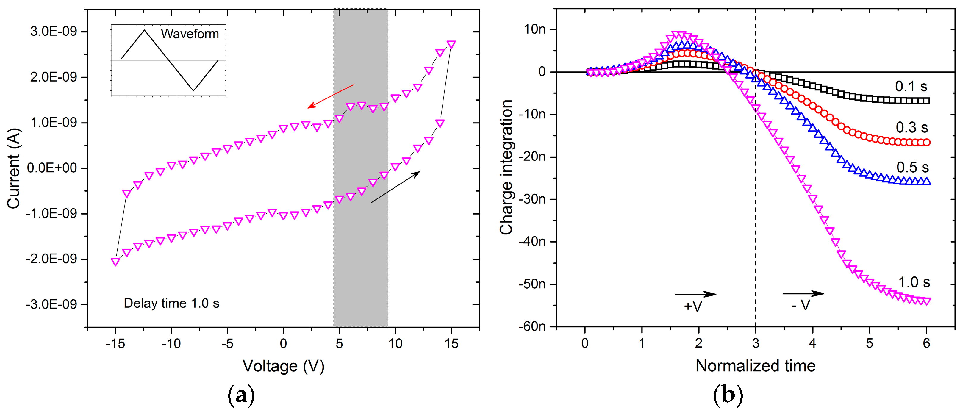
Next, we consider the change in conductivity and charge accumulation depending on the time the signal is applied. Figure 5 shows the current–voltage characteristics of the BFOT film structure measured at different voltage sweep rates (delay times). The presented I–V curves were obtained without prior electroforming of the sample. Figure 5a demonstrates that the sample’s current–voltage characteristics exhibit a hysteresis loop that passes through all four quadrants of the coordinates. As the voltage sweep rate increases, the hysteresis loop of the I–V slightly widens in the first and third quadrants due to an increase in the displacement current, which is determined as the time derivative of the electric displacement D [41]. Figure 5b shows the integral dependence of charge accumulation under positive and negative voltage polarities at different delay and release times. With an increase in the delay time up to 1 s, the current increases in both directions, which is characteristic of domain polarization.
The internal electric field is directed towards the external field, and at the point of intersection of the reverse I–V with the abscissa axis, it fully compensates for it. With further voltage reduction, the internal field prevails over the external one, and the current changes its direction to the opposite. The slight maximum at the initial part of the forward I–V for a delay time of 1.0 s is related to the switching of polarization domains in the ferroelectric along the external field. The BFOT possesses volumetric charge polarization due to its inhomogeneous dielectric structure, resulting in an internal field [16]. In turn, the internal field can influence the slope of the energy levels due to differences in the width of the forbidden zone, which varies in the range of 2.31–2.67 eV [42]. The phase transformation at the film-substrate interface creates defect regions and oxygen vacancies in the structure [35]. Such interface boundaries and defects can trap charge carriers under the application of an external field.
BFO exhibits piezoelectric properties, generating its own internal potential [43,44]. The film’s piezoelectric potential can increase depending on the applied displacement and light [45]. If the substrate has a bending property, mechanical stress can easily relax throughout its surface, creating non-uniform regions of voltage accumulation. This property of BFO is particularly useful for heterostructures with flexible substrates [46]. Figure 6 shows an SEM image of nanotube surfaces after deposition, where the film can press on the substrate and thereby spread out more free nanotubes.
The calculation results show that TiO2 (Nt) exhibits high values of Young’s modulus (800 GPa) outside the [47], plane, but the planar mechanical response of TiO2 (Nt) nanotube arrays is characterized by very low elastic moduli and significant damping [48]. Due to the surface’s heterogeneity with nanotubes, the film covers unevenly in thickness. As shown in Figure 6, in the pits area where a thicker section of the film is present, pressure can create deformations and partially shift the array of nanotubes. Non-uniform voltage accumulation regions are formed in the structure at the film-substrate interface. Figure 7 shows the PFM surface of the sample when applying a voltage of different polarity. Without applying voltage, the sample partially has a charge on the surface (Figure 7a). Applying positive voltage to the surface further enhances piezopolarization (Figure 7b). As seen from the figure, the sample possesses ferroelectric properties. Due to the complex morphology of the surface, domain boundaries have potential heterogeneity. Negative potential reduces surface charge.
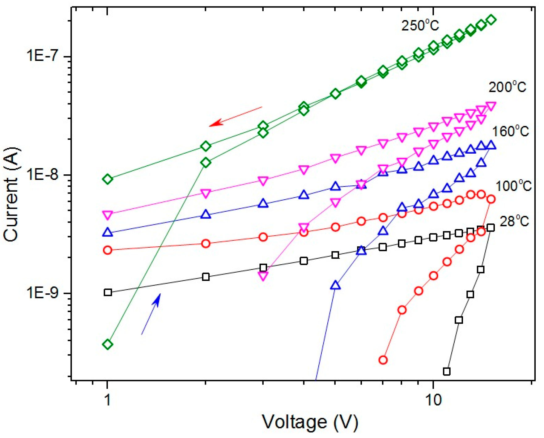
The charge moves through the inhomogeneities at the boundaries of the nanotubes, where the resistance is lower, vertically along the sample towards the bottom electrode. The surface remains partially positively charged. This indicates the polarization of domains in the surface film of BFO. To understand the mechanism of charge capture and release, we conducted temperature measurements. Figure 8 shows the dependence of I–V on temperature.
As seen from the figure, as the temperature increases, the I–V curve’s hysteresis loop narrows along the ordinate axis, while the current values around the loop increase, and at T = 250 °C, the loop almost collapses into a line, and the current value at the end of the forward I–V increases by two orders of magnitude for T = 28 °C. The increase in conductivity with increasing temperature is due to an increase in carrier concentration [49]. In turn, increasing conductivity hinders polarization processes in the dielectric (ferroelectric) since these are competing mechanisms; the internal field in the sample weakens as it heats up, ultimately leading to the collapse of the I–V loop [50]. During the formation of conducting channels in a semiconductor state, the isolating layer of the ferroelectric undergoes a soft breakdown, which causes a sharp current jump with subsequent voltage change. It was found that the current increased while the voltage on the sample decreased, which excluded a hard breakdown in the microstructure of the dielectric. A characteristic feature of the sample’s I(t) dependence on increasing temperature is the gradual decrease in current over time after applying a constant voltage with subsequent leveling off. The concept of the relaxation time of level filling τ determines the time that the current carrier spends at the trap energy level Et and the time it takes to empty it after the activation process is turned off/on, generally being a function of temperature. The time τ is related to the trap energy Et by the following relationship:
where σ is the cross-section, υT is the average relative velocity of charge thermal motion to the trap, and N is the concentration of traps (defects). During the formation of conducting channels in the semiconductor state, a soft breakdown occurs through the insulating layer, causing a sharp jump in current with subsequent voltage change [51]. It was found that the current increased while the voltage on the sample decreased, which excluded a hard breakdown in the microstructure of the dielectric. The increase and decrease in conductivity within the dielectric layer during the ascending and descending phases of the I–V occur due to the release of electrons at defect levels described by the Poole–Frenkel conduction mechanism [52]. Direct oscilloscope and pulsed measurements in low-resistance and intermediate states are needed for a more detailed assessment of level-filling relaxation time values.
4. Conclusions
The modification of the substrate surface of titanium dioxide nanotubes has shown a good phase interaction with the BFOT structure, which has controllable electrical characteristics. BFOT possesses both ferroelectric and semiconductor properties, with nonlinear conductivity dependent on the magnitude and duration of applied voltage. Temperature-dependent I–V curves have shown charge redistribution in the sample. During mutual diffusion of Ti↔Fe in the material, areas with non-uniform conductivity are formed. Structural defects and oxygen vacancies create levels in the forbidden band. These defects, in turn, participate in charge carrier capture and release processes. The increase and decrease in conductivity within the dielectric layer during the ascending and descending phases of the I–V curve occur due to the release of electrons from defect levels described by the Poole–Frenkel conduction mechanism.
Author Contributions
Conceptualization and methodology, S.R. and G.G.; software, F.O. and G.G.; formal analysis, F.O. and S.R.; data curation, S.R. and G.G.; writing—original draft, S.R.; writing—review and editing, S.R.; visualization, S.R., G.G. and F.O. All authors have read and agreed to the published version of the manuscript.
Funding
This work was supported by the Russian Science Foundations under grant 23-22-00421.
Institutional Review Board Statement
Not applicable.
Informed Consent Statement
Not applicable.
Data Availability Statement
The data that support the findings of this study are available from the corresponding author upon reasonable request.
Conflicts of Interest
The authors declare no conflict of interest.
References
- Cai, Y.; Zhang, J.; Yan, M.; Jiang, Y.; Jawad, H.; Tian, B.; Wang, W.; Zhan, Y.; Qin, Y.; Xiong, S.; et al. Molecular ferroelectric/semiconductor interfacial memristors for artificial synapses. NPJ Flex. Electron. 2022, 6, 16. [Google Scholar] [CrossRef]
- Zhao, Z.; Yan, X. Ferroelectric Memristor Based on Hf0.5Zr0.5O2 Thin Film Combining Memristive and Neuromorphic Functionalities. Phys. Status Solidi–Rapid Res. Lett. 2020, 14, 2000224. [Google Scholar] [CrossRef]
- Luk’yanchuk, I.; Razumnaya, A.; Sené, A.; Tikhonov, Y.; Vinokur, V.M. The ferroelectric field-effect transistor with negative capacitance. NPJ Comput. Mater. 2022, 8, 52. [Google Scholar] [CrossRef]
- Hoffman, J.; Pan, X.; Reiner, J.W.; Walker, F.J.; Han, J.P.; Ahn, C.H.; Ma, T.P. Ferroelectric Field Effect Transistors for Memory Applications. Adv. Mater. 2010, 22, 2957–2961. [Google Scholar] [CrossRef] [PubMed]
- Kim, J.Y.; Choi, M.J.; Jang, H.W. Ferroelectric field effect transistors: Progress and perspective. APL Mater. 2021, 9, 021102. [Google Scholar] [CrossRef]
- Panda, D.; Patnaik, A. Novel TiO2-based memristors FET with programmable SET/RESET for neuromorphic computing. Mater. Today Proc. 2023, in press. [Google Scholar] [CrossRef]
- Chen, A. A review of emerging non-volatile memory (NVM) technologies and applications. Solid. State. Electron. 2016, 125, 25–38. [Google Scholar] [CrossRef]
- Sun, G.; Zhao, J.; Poremba, M.; Xu, C.; Xie, Y. Memory that never forgets: Emerging nonvolatile memory and the implication for architecture design. Natl. Sci. Rev. 2018, 5, 577–592. [Google Scholar] [CrossRef]
- Cardona Rodríguez, A.; Reiber, A.; Schuller, I.K.; Muraca, D.; Gabriel Ramírez, J. Evidence of a glassy magnetic transition driven by structural disorder in BiFeO3 nanoparticles. J. Magn. Magn. Mater. 2022, 563, 169917. [Google Scholar] [CrossRef]
- Wang, J.; Neaton, J.B.; Zheng, H.; Nagarajan, V.; Ogale, S.B.; Liu, B.; Viehland, D.; Vaithyanathan, V.; Schlom, D.G.; Waghmare, U.V.; et al. Epitaxial BiFeO3 multiferroic thin film heterostructures. Science 2003, 299, 1719–1722. [Google Scholar] [CrossRef]
- Schmidt, R.; Eerenstein, W.; Winiecki, T.; Morrison, F.D.; Midgley, P.A. Impedance spectroscopy of epitaxial multiferroic thin films. Phys. Rev. B-Condens. Matter Mater. Phys. 2007, 75, 245111. [Google Scholar] [CrossRef]
- Tomczyk, M.; Mahajan, A.; Tkach, A.; Vilarinho, P.M. Interface-based reduced coercivity and leakage currents of BiFeO3 thin films: A comparative study. Mater. Des. 2018, 160, 1322–1334. [Google Scholar] [CrossRef]
- Wani, W.A.; Naaz, N.; Venkataraman, B.H.; Kundu, S.; Ramaswamy, K. Significantly reduced leakage current density in Mn-doped BiFeO3 thin films deposited using spin coating technique. J. Phys. Conf. Ser. 2021, 2070, 012088. [Google Scholar] [CrossRef]
- Tuluk, A.; Joshi, S.; Mahon, T.; Van Der Zwaag, S. Tuning piezoproperties of BiFeO3ceramic by cobalt and titanium dual doping. J. Appl. Phys. 2022, 131, 214104. [Google Scholar] [CrossRef]
- Zhao, Z.; Abdelsamie, A.; Guo, R.; Shi, S.; Zhao, J.; Lin, W.; Sun, K.; Wang, J.; Wang, J.; Yan, X.; et al. Flexible artificial synapse based on single-crystalline BiFeO3 thin film. Nano Res. 2022, 15, 2682–2688. [Google Scholar] [CrossRef]
- Illarionov, G.A.; Morozova, S.M.; Chrishtop, V.V.; Einarsrud, M.A.; Morozov, M.I. Memristive TiO2: Synthesis, Technologies, and Applications. Front. Chem. 2020, 8, 556815. [Google Scholar] [CrossRef]
- Adamaki, V.; Clemens, F.; Ragulis, P.; Pennock, S.R.; Taylor, J.; Bowen, C.R. Manufacturing and characterization of Magnéli phase conductive fibres. J. Mater. Chem. A 2014, 2, 8328–8333. [Google Scholar] [CrossRef]
- Ramazanov, S.; Sobola, D.; Ţălu, Ş.; Orudzev, F.; Arman, A.; Kaspar, P.; Dallaev, R.; Ramazanov, G. Multiferroic behavior of the functionalized surface of a flexible substrate by deposition of Bi2O3 and Fe2O3. Microsc. Res. Tech. 2022, 85, 1300–1310. [Google Scholar] [CrossRef]
- Ramazanov, S.; Ţălu, Ş.; Sobola, D.; Orudzev, F.; Ramazanov, G.; Selimov, D.; Kaspar, P.; Macků, R.; Nazarov, A. Crack resistance of bismuth ferrite films obtained on a flexible substrate. E3S Web Conf. 2021, 295, 04008. [Google Scholar] [CrossRef]
- Cai, S.; Lun, Y.; Ji, D.; Lv, P.; Han, L.; Guo, C.; Zang, Y.; Gao, S.; Wei, Y.; Gu, M.; et al. Enhanced polarization and abnormal flexural deformation in bent freestanding perovskite oxides. Nat. Commun. 2022, 13, 5116. [Google Scholar] [CrossRef] [PubMed]
- Guo, R.; You, L.; Lin, W.; Abdelsamie, A.; Shu, X.; Zhou, G.; Chen, S.; Liu, L.; Yan, X.; Wang, J.; et al. Continuously controllable photoconductance in freestanding BiFeO3 by the macroscopic flexoelectric effect. Nat. Commun. 2020, 11, 2571. [Google Scholar] [CrossRef]
- Ramazanov, S.; Orudzhev, F.; Gajiev, G.; Holcman, V.; Matos, R.S.; da Fonseca Filho, H.D.; Ţălu, Ş.; Selimov, D. Local electrical characteristic of memristor structure in a high-resistance state obtained using electrostatic force microscopy: Fractal and multifractal dynamics of surface. Appl. Surf. Sci. 2023, 647, 158863. [Google Scholar] [CrossRef]
- Min, Y.-S.; Cho, Y.J.; Ko, J.-H.; Bae, E.J.; Park, W.; Hwang, C.S. Atomic Layer Deposition of Bi1−x−yTixSiyOz Thin Films from Alkoxide Precursors and Water. J. Electrochem. Soc. 2005, 152, F124. [Google Scholar] [CrossRef]
- Martinson, A.B.F.; DeVries, M.J.; Libera, J.A.; Christensen, S.T.; Hupp, J.T.; Pellin, M.J.; Elam, J.W. Atomic Layer Deposition of Fe2O3 Using Ferrocene and Ozone. J. Phys. Chem. C 2011, 115, 4333–4339. [Google Scholar] [CrossRef]
- Lie, M.; Fjellvåg, H.; Kjekshus, A. Growth of Fe2O3 thin films by atomic layer deposition. Thin Solid Films 2005, 488, 74–81. [Google Scholar] [CrossRef]
- Akbashev, A.R.; Chen, G.; Spanier, J.E. A Facile Route for Producing Single-Crystalline Epitaxial Perovskite Oxide Thin Films. Nano Lett. 2014, 14, 44–49. [Google Scholar] [CrossRef]
- Ivanov, S.A.; Sarkar, T.; Fortalnova, E.A.; Politova, E.D.; Stefanovich, S.Y.; Safronenko, M.G.; Nordblad, P.; Mathieu, R. Composition dependence of the multifunctional properties of Nd-doped Bi4Ti3O12 ceramics. J. Mater. Sci. Mater. Electron. 2017, 28, 7692–7707. [Google Scholar] [CrossRef]
- Zhang, S.T.; Lu, M.H.; Wu, D.; Chen, Y.F.; Ming, N.B. Larger polarization and weak ferromagnetism in quenched BiFeO3 ceramics with a distorted rhombohedral crystal structure. Appl. Phys. Lett. 2005, 87, 262907. [Google Scholar] [CrossRef]
- Lisińska-Czekaj, A.; Lubina, M.; Czekaj, D.; Rerak, M.; Garbarz-Glos, B.; Bąk, W. Influence of Processing Conditions on Crystal Structure of Bi6Fe2Ti3O18 Ceramics. Arch. Metall. Mater. 2016, 61, 881–886. [Google Scholar] [CrossRef]
- Tian, F.; Zhang, Y.; Zhang, J.; Pan, C. Raman Spectroscopy: A New Approach to Measure the Percentage of Anatase TiO2 Exposed (001) Facets. J. Phys. Chem. C 2012, 116, 7515–7519. [Google Scholar] [CrossRef]
- Tompsett, G.A.; Bowmaker, G.A.; Cooney, R.P.; Metson, J.B.; Rodgers, K.A.; Seakins, J.M. The Raman spectrum of brookite, TiO2 (Pbca, Z = 8). J. Raman Spectrosc. 1995, 26, 57–62. [Google Scholar] [CrossRef]
- Kooriyattil, S.; Pavunny, S.P.; Barrionuevo, D.; Katiyar, R.S. Optical, ferroelectric, and piezoresponse force microscopy studies of pulsed laser deposited Aurivillius Bi5FeTi3O15 thin films. J. Appl. Phys. 2014, 116, 144101. [Google Scholar] [CrossRef]
- Lomanova, N.A. Aurivillius Phases Bim + 1Fem – 3Ti3O3m + 3: Synthesis, Structure, and Properties (a Review). Russ. J. Inorg. Chem. 2022, 67, 741–753. [Google Scholar] [CrossRef]
- Lu, C.D.; Chang, L.S.; Lu, Y.F.; Lu, F.H. The growth of interfacial compounds between titanium dioxide and bismuth oxide. Ceram. Int. 2009, 35, 2699–2704. [Google Scholar] [CrossRef]
- Orudzhev, F.F.; Ramazanov, S.M.; Isaev, A.B.; Alikhanov, N.M.R.; Sobola, D.; Presniakov, M.Y.; Kaviyarasu, K. Self-organization of layered perovskites on TiO2 nanotubes surface by atomic layer deposition. Mater. Today Proc. 2021, 36, 364–367. [Google Scholar] [CrossRef]
- Sun, S.; Chen, Z.; Wang, G.; Geng, X.; Xiao, Z.; Sun, Z.; Sun, Z.; Peng, R.; Lu, Y. Nanoscale Structural Modulation and Low-temperature Magnetic Response in Mixed-layer Aurivillius-type Oxides. Sci. Rep. 2018, 8, 871. [Google Scholar] [CrossRef] [PubMed]
- Sun, S.; Wang, G.; Huang, Y.; Wang, J.; Peng, R.; Lu, Y. Structural transformation and multiferroic properties in Gd-doped Bi7Fe3Ti3O21 ceramics. RSC Adv. 2014, 4, 30440–30446. [Google Scholar] [CrossRef]
- Sun, S.; Yan, H.; Wang, G.; Wang, J.; Peng, R.; Fu, Z.; Zhai, X.; Mao, X.; Chen, X.; Lu, Y. Room-temperature multiferroic responses arising from 1D phase modulation in correlated Aurivillius-type layer structures. J. Phys. D Appl. Phys. 2016, 49, 125005. [Google Scholar] [CrossRef]
- Armstrong, R.A.; Newnham, R.E. Bismuth titanate solid solutions. Mater. Res. Bull. 1972, 7, 1025–1034. [Google Scholar] [CrossRef]
- Kikuchi, T. Stability of layered bismuth compounds in relation to the structural mismatch. Mater. Res. Bull. 1979, 14, 1561–1569. [Google Scholar] [CrossRef]
- Yan, H.; Inam, F.; Viola, G.; Ning, H.; Zhang, H.; Jiang, Q.; Zeng, T.A.O.; Gao, Z.; Reece, M.J. The Contribution of Electrical Conductivity, Dielectric Permittivity and Domain Switching in Ferroelectric Hysteresis Loops. J. Adv. Dielectr. 2011, 01, 107–118. [Google Scholar] [CrossRef]
- Orudzhev, F.; Ramazanov, S.; Sobola, D.; Isaev, A.; Wang, C.; Magomedova, A.; Kadiev, M.; Kaviyarasu, K. Atomic layer deposition of mixed-layered aurivillius phase on TIO2 nanotubes: Synthesis, characterization and photoelectrocatalytic properties. Nanomaterials 2020, 10, 2183. [Google Scholar] [CrossRef] [PubMed]
- Orudzhev, F.; Ramazanov, S.; Sobola, D.; Alikhanov, N.; Holcman, V.; Škvarenina, L.; Kaspar, P.; Gadjilov, G. Piezoelectric Current Generator Based on Bismuth Ferrite Nanoparticles. Sensors 2020, 20, 6736. [Google Scholar] [CrossRef] [PubMed]
- Yao, Y.; Chen, L.; Wang, Z.; Alshareef, H.; Zhang, X.X. Electrical and piezoelectric properties of BiFeO 3 thin films grown on SrxCa1−xRuO3-buffered SrTiO3 substrates. J. Appl. Phys. 2012, 111, 114102. [Google Scholar] [CrossRef]
- Heo, Y.; Zhang, H.; Alexe, M. Dynamic Control of Piezoelectricity Enhancement via Modulation of the Bulk Photovoltaic Effect in a BiFeO3 Thin Film. Adv. Electron. Mater. 2022, 8, 2200785. [Google Scholar] [CrossRef]
- Ramazanov, S.; Sobola, D.; Gajiev, G.; Orudzhev, F.; Kaspar, P.; Gummetov, A. Multiferroic/Polymer Flexible Structures Obtained by Atomic Layer Deposition. Nanomaterials 2022, 13, 139. [Google Scholar] [CrossRef]
- Xu, Y.; Wang, M.; Hu, N.; Bell, J.; Yan, C. Atomistic investigation into the mechanical behaviour of crystalline and amorphous TiO2 nanotubes. RSC Adv. 2016, 6, 28121–28129. [Google Scholar] [CrossRef]
- Fischer, K.; Mayr, S.G. In-Plane Mechanical Response of TiO2 Nanotube Arrays—Intrinsic Properties and Impact of Adsorbates for Sensor Applications. Adv. Mater. 2011, 23, 3838–3841. [Google Scholar] [CrossRef]
- Quddus, M.T.; Mudholkar, M.; Salih, A. Carrier separation technique to optimize conductivity modulation in high voltage rectifiers. In Proceedings of the 2015 IEEE International Conference on Electron Devices and Solid-State Circuits (EDSSC), Singapore, 1–4 June 2015; IEEE: Piscataway, NJ, USA, 2015; pp. 507–510. [Google Scholar]
- Paul, F.; Nama Manjunatha, K.; Paul, S. Non-Zero and Open-Loop Current–Voltage Characteristics in Electronic Memory Devices. Adv. Electron. Mater. 2023, 9, 2300324. [Google Scholar] [CrossRef]
- Pompl, T.; Engel, C.; Wurzer, H.; Kerber, M. Soft breakdown and hard breakdown in ultra-thin oxides. Microelectron. Reliab. 2001, 41, 543–551. [Google Scholar] [CrossRef]
- Funck, C.; Menzel, S. Comprehensive Model of Electron Conduction in Oxide-Based Memristive Devices. ACS Appl. Electron. Mater. 2021, 3, 3674–3692. [Google Scholar] [CrossRef]
Figure 1.
Scheme of atomic layer deposition of a heterostructure in the BiOx/FeOx/TiO2(Nt)/Ti system.
Figure 1.
Scheme of atomic layer deposition of a heterostructure in the BiOx/FeOx/TiO2(Nt)/Ti system.

Figure 2.
SEM of surfaces before and after application of BFO film, vertical and horizontal profile along a line showing the closure of almost all pores.
Figure 2.
SEM of surfaces before and after application of BFO film, vertical and horizontal profile along a line showing the closure of almost all pores.
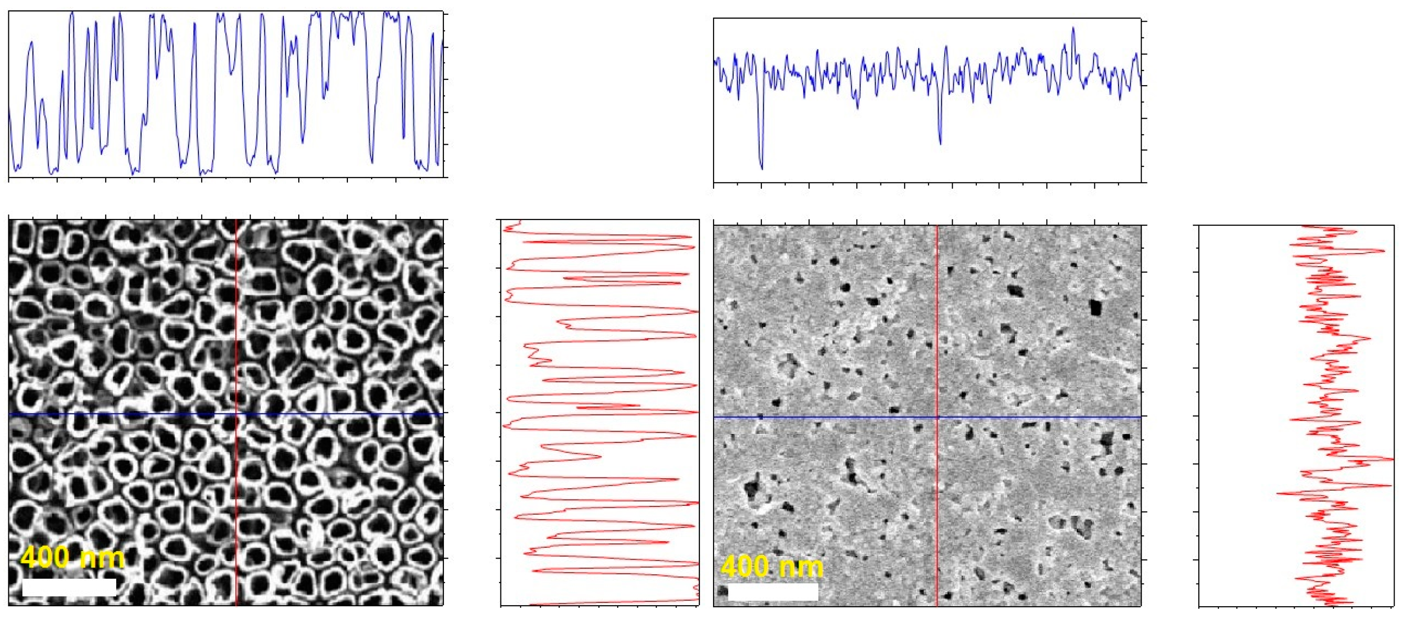
Figure 3.
XRD patterns of TiO2(Nt)/Ti (bottom) and BFOT (top). A—anatase; R—rutile; Ti—titanium; *—Bi4Ti3O12; the tabs show the phases Bi6Fe2Ti3O18 and BiFeO3.
Figure 3.
XRD patterns of TiO2(Nt)/Ti (bottom) and BFOT (top). A—anatase; R—rutile; Ti—titanium; *—Bi4Ti3O12; the tabs show the phases Bi6Fe2Ti3O18 and BiFeO3.

Figure 4.
Raman spectra of the nanotube substrate (bottom) and the BFO film (top).
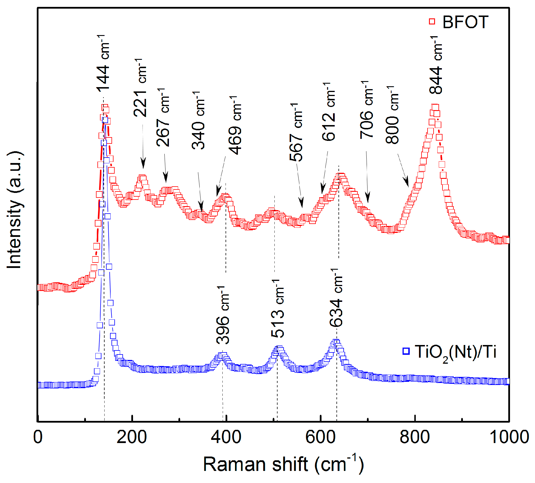
Figure 5.
Current-voltage characteristic of the sample, arrows indicate the direction of voltage application, delay time 0.1 s (a). Dependence of the integral charge, normalized by time, measured with different delay times 0.1, 0.3, 0.5, 1.0 s (b).
Figure 5.
Current-voltage characteristic of the sample, arrows indicate the direction of voltage application, delay time 0.1 s (a). Dependence of the integral charge, normalized by time, measured with different delay times 0.1, 0.3, 0.5, 1.0 s (b).

Figure 6.
SEM image of nanotubes before (top) and after (bottom) deposition of the BFO film, the lines show how the TiO2(Nt) nanotubes are deformed.
Figure 6.
SEM image of nanotubes before (top) and after (bottom) deposition of the BFO film, the lines show how the TiO2(Nt) nanotubes are deformed.

Figure 7.
PFM of the film surface without applying voltage (a). When applying voltage 5V and −5V (b).
Figure 7.
PFM of the film surface without applying voltage (a). When applying voltage 5V and −5V (b).
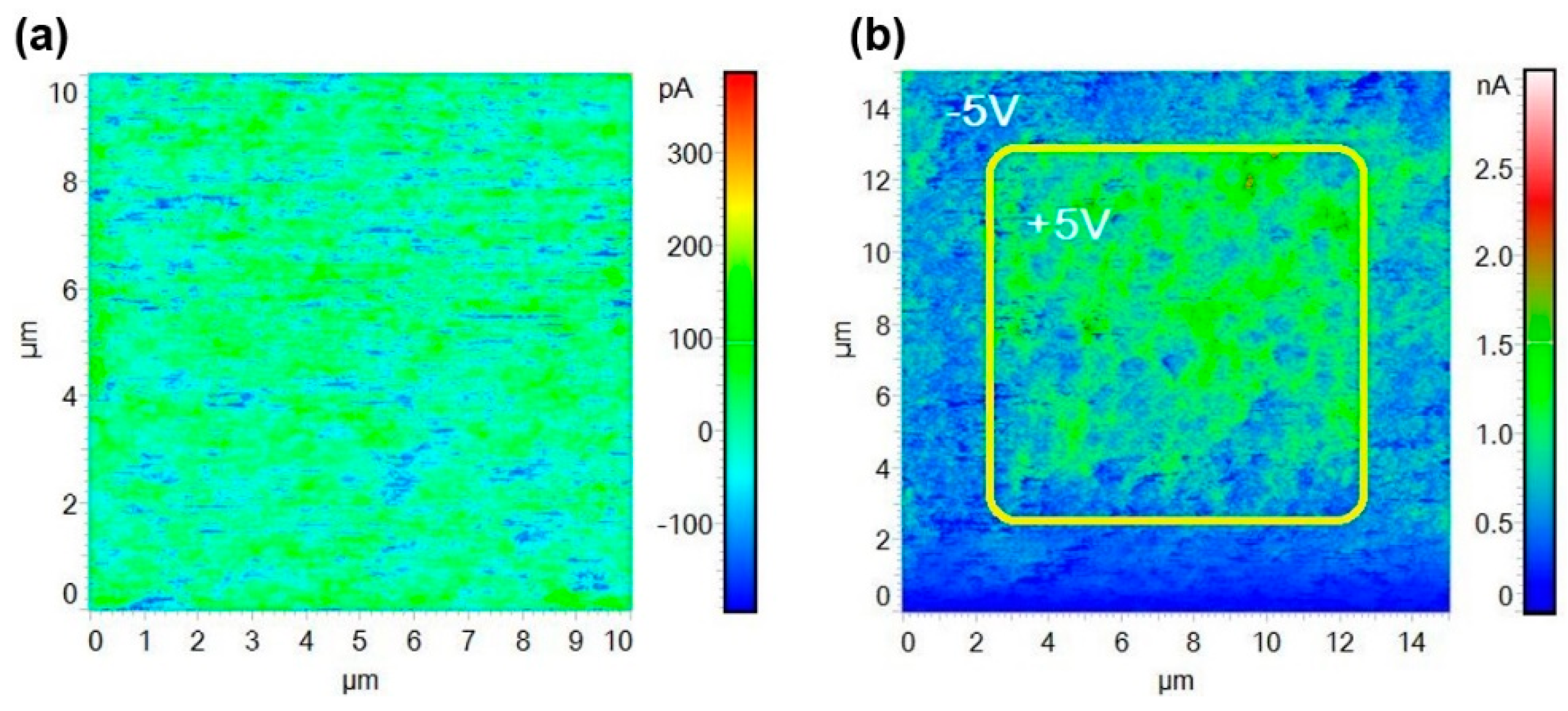
Figure 8.
Current-voltage characteristics on a logarithmic scale at various temperatures, delay time t = 0.1 s.
Figure 8.
Current-voltage characteristics on a logarithmic scale at various temperatures, delay time t = 0.1 s.
Disclaimer/Publisher’s Note: The statements, opinions and data contained in all publications are solely those of the individual author(s) and contributor(s) and not of MDPI and/or the editor(s). MDPI and/or the editor(s) disclaim responsibility for any injury to people or property resulting from any ideas, methods, instructions or products referred to in the content. |
© 2023 by the authors. Licensee MDPI, Basel, Switzerland. This article is an open access article distributed under the terms and conditions of the Creative Commons Attribution (CC BY) license (https://creativecommons.org/licenses/by/4.0/).
Share and Cite
MDPI and ACS Style
Ramazanov, S.; Orudzhev, F.; Gajiev, G. Surface Functionalization of TiO2 Nanotubes Modified with a Thin Film of BiFeO3. Surfaces 2024, 7, 1-11. https://doi.org/10.3390/surfaces7010001
AMA Style
Ramazanov S, Orudzhev F, Gajiev G. Surface Functionalization of TiO2 Nanotubes Modified with a Thin Film of BiFeO3. Surfaces. 2024; 7(1):1-11. https://doi.org/10.3390/surfaces7010001
Chicago/Turabian StyleRamazanov, Shikhgasan, Farid Orudzhev, and Gaji Gajiev. 2024. "Surface Functionalization of TiO2 Nanotubes Modified with a Thin Film of BiFeO3" Surfaces 7, no. 1: 1-11. https://doi.org/10.3390/surfaces7010001