
Recent Excellent Optoelectronic Applications Based on Two-Dimensional WS2 Nanomaterials: A Review

Abstract
:1. Introduction
2. Preparation of 2D WS2
3. Optoelectronic Applications Based on WS2 Devices
3.1. LEDs
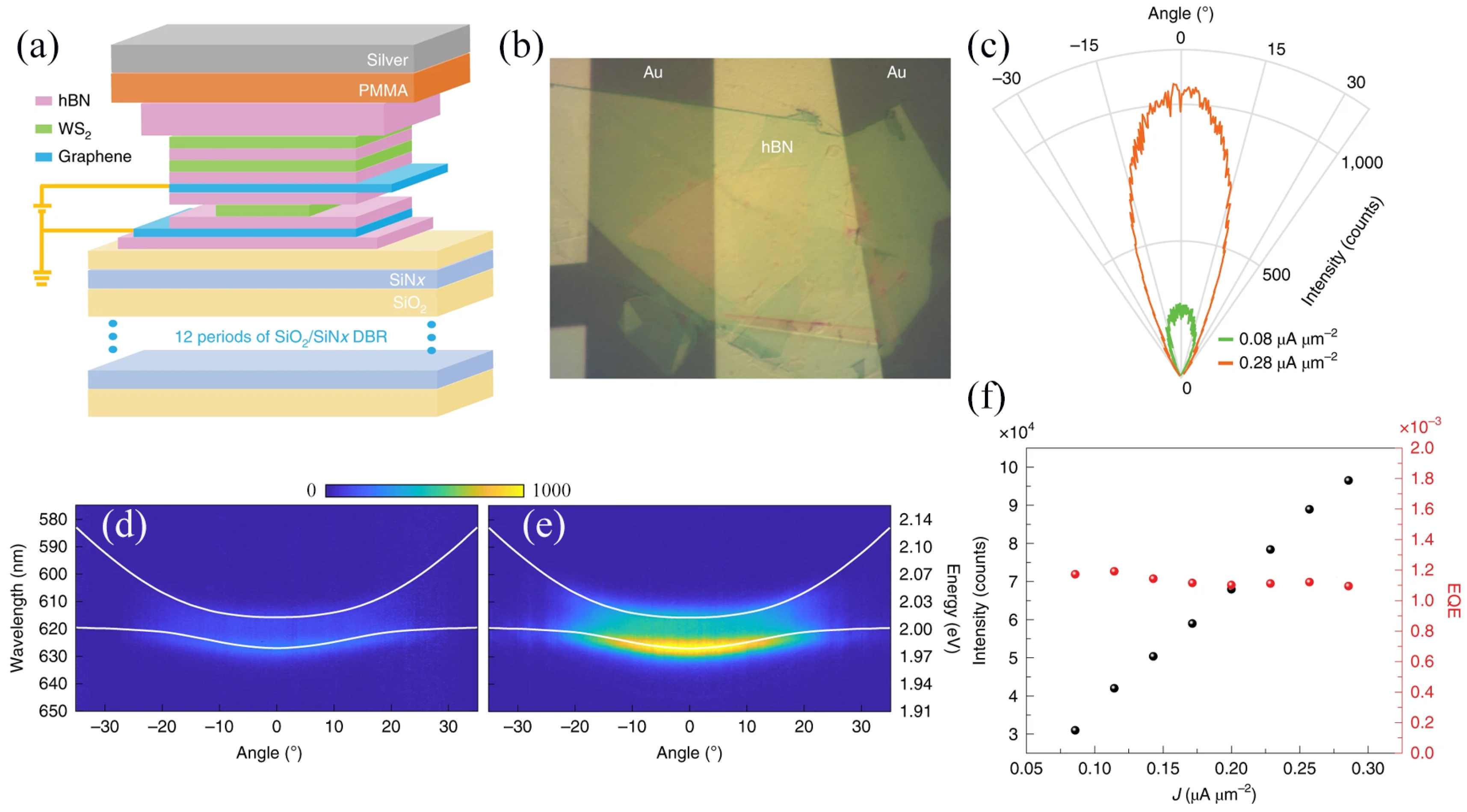
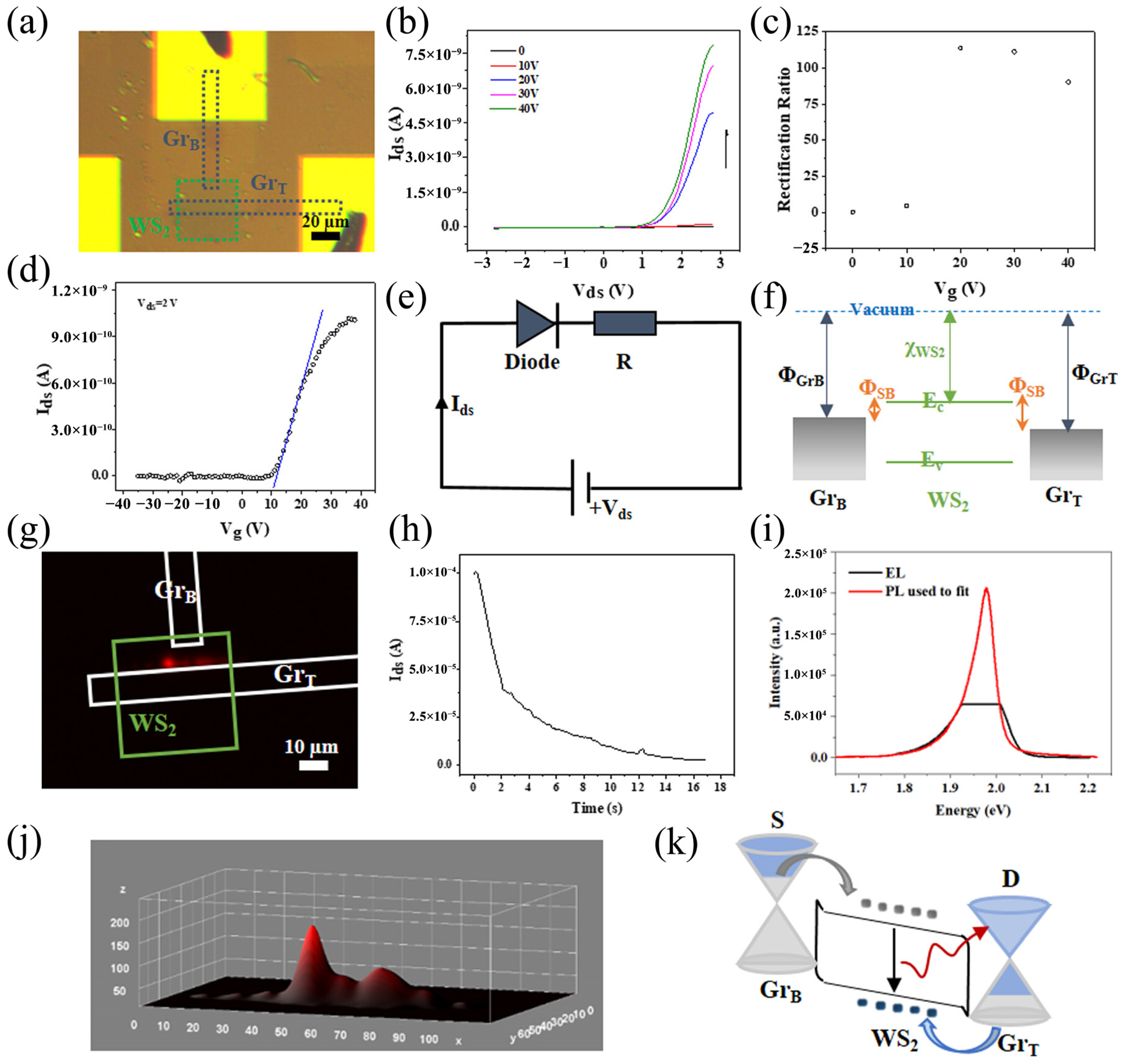
3.1.1. Polarized LEDs
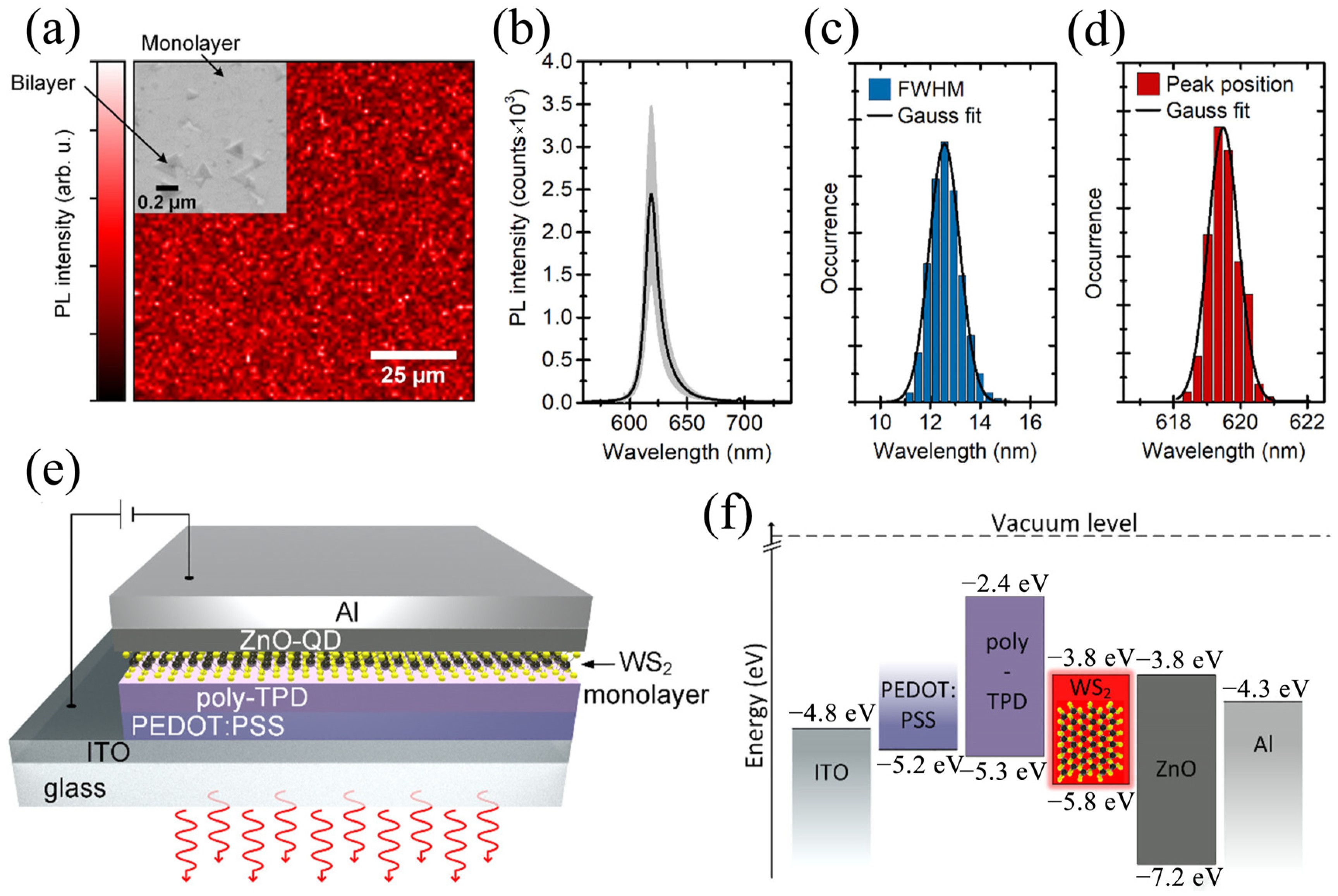
3.1.2. Ordinary Monochrome LEDs
3.1.3. Wavelength Adjustable LEDs
3.1.4. Summary
3.2. Sensors
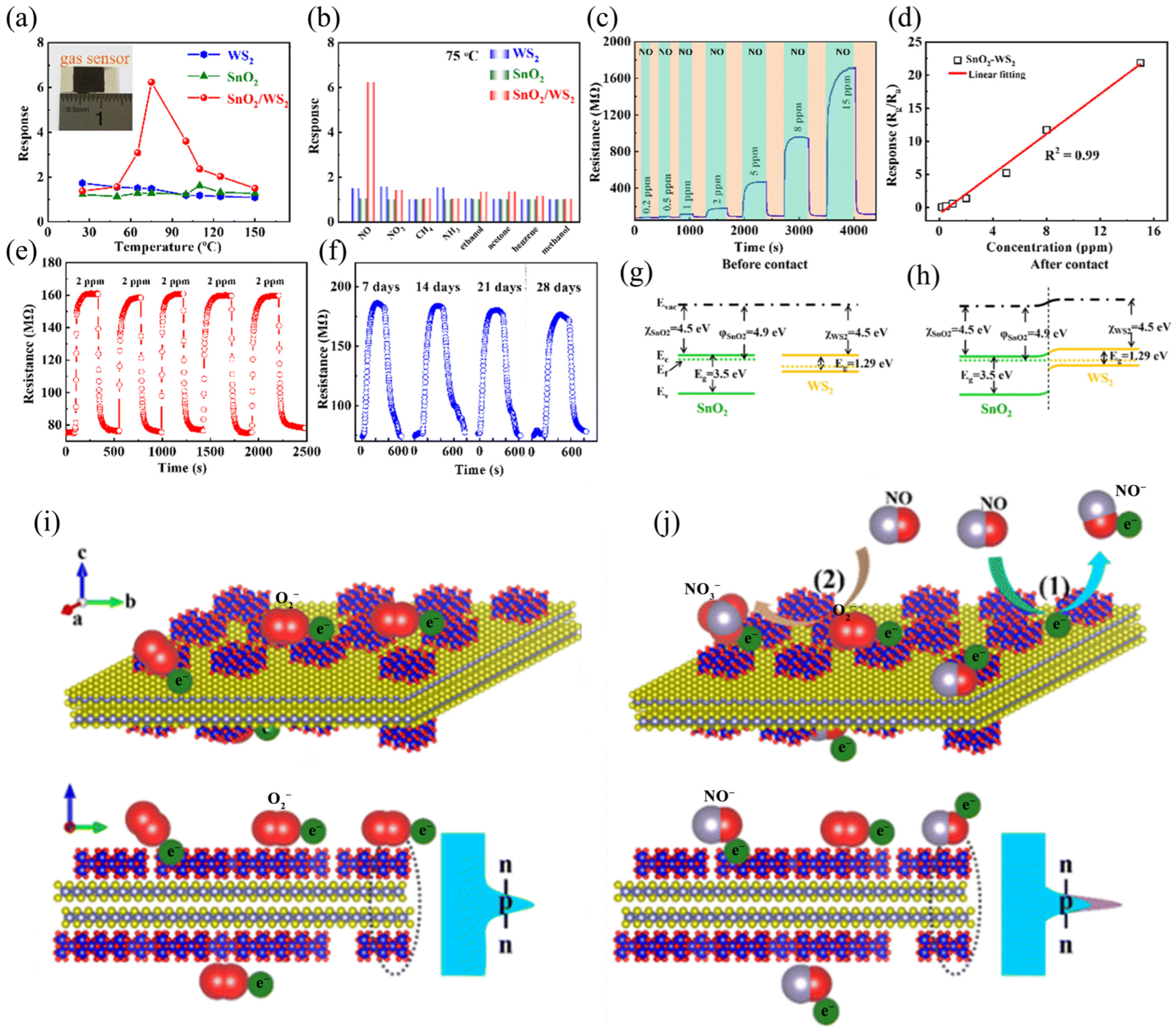
3.2.1. Gas Sensors
3.2.2. Flexible Sensors
3.2.3. Summary
3.3. Transistors
3.3.1. Ordinary Metal-Oxide–Semiconductor FETs
3.3.2. Metal–Insulator–Semiconductor Contact FETs
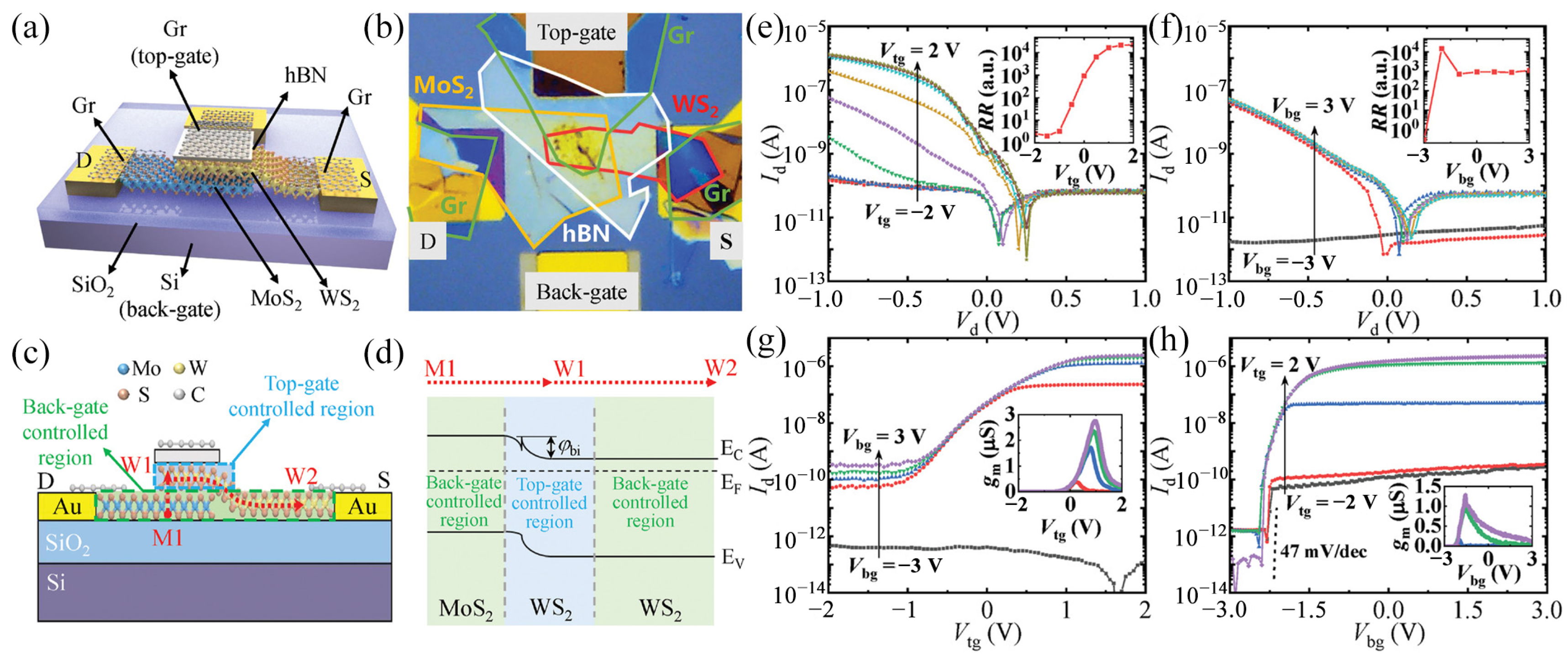
3.3.3. Dual Door Control FETs
3.3.4. WS2 P-Type Channel FETs
3.3.5. Synaptic Transistors
3.3.6. Phototransistors
3.3.7. Summary
3.4. Photodetectors
3.4.1. Flexible Photodetectors
3.4.2. Wide-Spectrum Photodetectors
3.4.3. Infrared Photodetectors
3.4.4. Ultraviolet Photodetectors
3.4.5. Summary
3.5. Field Emission
3.5.1. Field Emission Devices
3.5.2. Summary
3.6. Memory Devices
3.6.1. Non-Volatile Memory Devices
3.6.2. Summary
4. Optoelectronic Applications of Other TMD Materials
5. Conclusions and Outlook
Author Contributions
Funding
Institutional Review Board Statement
Informed Consent Statement
Data Availability Statement
Conflicts of Interest
References
- Thakur, D.; Kumar, P.; Sabarigresan, M. Layer number dependent optical and electrical properties of CVD grown two-dimensional anisotropic WS2. Surf. Interfaces 2021, 26, 101308. [Google Scholar] [CrossRef]
- Yang, H.; Wang, Y.; Zou, X. Growth mechanisms and morphology engineering of atomic layer-deposited WS2. ACS Appl. Mater. Interfaces 2021, 13, 43115–43122. [Google Scholar] [CrossRef]
- Wang, Y.; Sohier, T.; Watanabe, K. Electron mobility in monolayer WS2 encapsulated in hexagonal boron-nitride. Appl. Phys. Lett. 2021, 118, 102105. [Google Scholar] [CrossRef]
- Guo, S.; Guo, H.; Wang, X. Synthesis and electrochemical performance of WS2 nanosheet for thermal batteries. Mater. Lett. 2019, 249, 81–83. [Google Scholar] [CrossRef]
- Kumari, S.; Chouhan, A.; Sharma, O.P. Surface functionalization of WS2 nanosheets with alkyl chains for enhancement of dispersion stability and tribological properties. ACS Appl. Mater. Interfaces 2021, 14, 1334–1346. [Google Scholar] [CrossRef]
- Lan, C.; Li, C.; Ho, J.C. 2D WS2: From vapor phase synthesis to device applications. Adv. Electron. Mater. 2021, 7, 2000688. [Google Scholar] [CrossRef]
- Ernandes, C.; Khalil, L.; Henck, H. Strain and spin-orbit coupling engineering in twisted WS2/graphene heterobilayer. Nanomaterials 2021, 11, 2921. [Google Scholar] [CrossRef]
- Kolesnik, D.L.; Pyaskovskaya, O.N.; Gnatyuk, O.P.; Cherepanov, V.V.; Karakhim, S.O.; Polovii, I.O.; Posudievsky, Y.O.; Konoshchuk, N.V.; Strelchuk, V.V.; Nikolenko, A.S.; et al. The effect of 2D tungsten disulfide nanoparticles on Lewis lung carcinoma cells in vitro. RSC Adv. 2021, 11, 16142–16150. [Google Scholar] [CrossRef]
- Jariwala, D.; Marks, T.J.; Hersam, M.C. Mixed-dimensional van der Waals heterostructures. Nat. Mater. 2017, 16, 170–181. [Google Scholar] [CrossRef]
- Cheng, Z.; Song, X.; Jiang, L.; Wang, L.; Sun, J.; Yang, Z.; Jian, Y.; Zhang, S.; Chen, X.; Zeng, H. A mixed-dimensional WS2/GaSb heterojunction for high-performance p–n diodes and junction field-effect transistors. J. Mater. Chem. C 2022, 10, 1511–1516. [Google Scholar] [CrossRef]
- Bora, A.; Mawlong, L.P.L.; Mia, A.K. Manipulating Trion and Biexciton Emissions in Monolayer WS2 by Sandwiching with Ultrathin ZnO Layers for Excitonic Light Emission Applications. ACS Appl. Nano Mater. 2024, 7, 8612–8623. [Google Scholar] [CrossRef]
- Phogat, P.; Jha, R.; Singh, S. Electrochemical analysis of hydrothermally synthesized 2D/1D WS2/WO3 nanocomposites for solar cell application. J. Phys. Chem. Solids 2024, 192, 112110. [Google Scholar]
- Dave, M.; Shah, P.V.; Anuraag, N.S. based flexible photodetector functionalized by WS2/Ti3C2Tx 2D-2D heterostructures. Opt.Mater. 2024, 150, 115244. [Google Scholar] [CrossRef]
- Wang, J.C.; Wang, X.P.; Li, X.D. Enhanced field emission characteristics of WS2 nano-films by diamond film and Mo film. Vacuum 2024, 225, 113223. [Google Scholar] [CrossRef]
- Mia, A.K.; Meyyappan, M.; Giri, P.K. Asymmetric contact-induced selective doping of CVD-grown bilayer WS2 and its application in high-performance photodetection with an ultralow dark current. Nanoscale 2024, 16, 8583–8596. [Google Scholar] [CrossRef]
- Roy, S.; Yang, X.; Gao, J. Biaxial strain tuned upconversion photoluminescence of monolayer WS2. Sci. Rep. 2024, 14, 3860. [Google Scholar] [CrossRef]
- Ghaffar, A.; Mohapatra, N.R.; Maezono, R. Substitutional Doping Strategies for Fermi Level Depinning and Enhanced Interface Quality in WS2-Metal Contacts. ACS Appl. Electron. Mater. 2024, 6, 4587–4600. [Google Scholar] [CrossRef]
- Hang, D.R.; Sun, D.Y.; Chen, C.H. Facile bottom-up preparation of WS2-based water-soluble quantum dots as luminescent probes for hydrogen peroxide and glucose. Nanoscale Res. Lett. 2019, 14, 1–15. [Google Scholar] [CrossRef]
- Gutiérrez-Cruz, A.; Ruiz-Hernández, A.R.; Vega-Clemente, J.F. A review of top-down and bottom-up synthesis methods for the production of graphene, graphene oxide and reduced graphene oxide. J. Mat. Sci. 2022, 57, 14543–14578. [Google Scholar] [CrossRef]
- Tizhoosh, N.Y.; Khataee, A.; Hassandoost, R. Ultrasound-engineered synthesis of WS2@ CeO2 heterostructure for sonocatalytic degradation of tylosin. Ultrason. Sonochem. 2020, 67, 105114. [Google Scholar] [CrossRef]
- Kim, J.Y.; Chae, S.; Jang, W. Antioxidant triggered metallic 1T’phase transformations of chemically exfoliated tungsten disulfide (WS2) nanosheets. Small 2022, 18, 2107557. [Google Scholar] [CrossRef]
- Islam, M.A.; Serles, P.; Kumral, B. Exfoliation mechanisms of 2D materials and their applications. Appl. Phys. Rev. 2022, 9, 041301. [Google Scholar] [CrossRef]
- Sharma, S.; Bhagat, S.; Singh, J. Excitation-dependent photoluminescence from WS2 nanostructures synthesized via top-down approach. J. Mater. Sci. 2017, 52, 11326–11336. [Google Scholar] [CrossRef]
- Sethulekshmi, A.S.; Jayan, J.S.; Saritha, A. Insights into the reinforcibility and multifarious role of WS2 in polymer matrix. J. Alloys Compd. 2021, 876, 160107. [Google Scholar] [CrossRef]
- Yang, D.; Frindt, R.F. Li-intercalation and exfoliation of WS2. J. Phys. Chem. Solids 1996, 57, 1113–1116. [Google Scholar] [CrossRef]
- Tsai, H.L.; Heising, J.; Schindler, J.L.; Kannewurf, C.R.; Kanatzidis, M.G. Exfoliated—Restacked phase of WS2. Chem. Mater. 1997, 9, 879–882. [Google Scholar] [CrossRef]
- Abid, N.; Khan, A.M.; Shujait, S. Synthesis of nanomaterials using various top-down and bottom-up approaches, influencing factors, advantages, and disadvantages: A review. Adv. Colloid Interface Sci. 2022, 300, 102597. [Google Scholar] [CrossRef]
- Liu, S.; Zeng, Y.; Zhang, M. Binder-free WS2 nanosheets with enhanced crystallinity as a stable negative electrode for flexible asymmetric supercapacitors. J. Mater. Chem. A 2017, 5, 21460–21466. [Google Scholar] [CrossRef]
- Cao, S.; Liu, T.; Hussain, S. Hydrothermal synthesis of variety low dimensional WS2 nanostructures. Mater. Lett. 2014, 129, 205–208. [Google Scholar] [CrossRef]
- Ding, C.; Zhao, C.; Cheng, S. Ultrahigh photocatalytic hydrogen evolution performance of coupled 1D CdS/1T-phase dominated 2D WS2 nanoheterojunctions. Chin. J. Catal. 2022, 43, 403–409. [Google Scholar] [CrossRef]
- Zhang, Z.; Chen, P.; Yang, X. Ultrafast growth of large single crystals of monolayer WS2 and WSe2. Natl. Sci. Rev. 2020, 7, 737–744. [Google Scholar] [CrossRef] [PubMed]
- Fan, Y.; Li, J.; Hao, G. Synthesis, characterization of WS2 nanostructures by vapor phase deposition. J. Appl. Phys. 2015, 117, 064302. [Google Scholar] [CrossRef]
- Yang, W.; Shang, J.; Wang, J.; Shen, X.; Cao, B.; Peimyoo, N.; Zou, C.; Chen, Y.; Wang, Y.; Cong, C.; et al. Electrically Tunable Valley-Light Emitting Diode (vLED) Based on CVD-Grown Monolayer WS2. Nano Lett. 2016, 16, 1560–1567. [Google Scholar] [CrossRef]
- Kim, C.; Nguyen, T.P.; Le, Q.V.; Jeon, J.; Jang, H.W.; Kim, S.Y. Performances of Liquid-Exfoliated Transition Metal Dichalcogenides as Hole Injection Layers in Organic Light-Emitting Diodes. Adv. Funct. Mater. 2015, 25, 4512–4519. [Google Scholar] [CrossRef]
- Zhao, W.; Ghorannevis, Z.; Chu, L.; Tho, M.; Kloc, C.; Tan, P.; Eda, G. Evolution of Electronic Structure in Atomically Thin Sheets of WS2 and WSe2. ACS Nano 2013, 7, 791–797. [Google Scholar] [CrossRef]
- Gu, J.; Chakraborty, B.; Khatoniar, M.; Menon, V.M. A room-temperature polariton light-emitting diode based on monolayer WS2. Nat. Nanotechnol. 2019, 14, 1024–1028. [Google Scholar] [CrossRef] [PubMed]
- Pu, J.; Zhang, W.; Matsuoka, H.; Kobayashi, Y.; Takaguchi, Y.; Miyata, Y.; Matsuda, K.; Miyauchi, Y.; Takenobu, T. Room-Temperature Chiral Light-Emitting Diode Based on Strained Monolayer Semiconductors. Adv. Mater. 2021, 33, 2100601. [Google Scholar] [CrossRef] [PubMed]
- Andrzejewski, D.; Myja, H.; Heuken, M.; Grundmann, A.; Kalisch, H.; Vescan, A.; Kümmell, T.; Bacher, G. Scalable Large-Area p–i–n Light-Emitting Diodes Based on WS2 Monolayers Grown via MOCVD. ACS Photon. 2019, 6, 1832–1839. [Google Scholar] [CrossRef]
- Zhang, Q.; Hou, L.; Shautsova, V.; Warner, J.H. Ultrathin All-2D Lateral Diodes Using Top and Bottom Contacted Laterally Spaced Graphene Electrodes to WS2 Semiconductor Monolayers. ACS Appl. Mater. Interfaces 2023, 15, 18012–18021. [Google Scholar] [CrossRef]
- Zhu, Y.; Wang, B.; Li, Z.; Zhang, J.; Tang, Y.; Torres, J.F.; Lipiński, W.; Fu, L.; Lu, Y. A High-Efficiency Wavelength-Tunable Monolayer LED with Hybrid Continuous-Pulsed Injection. Adv. Mater. 2021, 33, 2101375. [Google Scholar] [CrossRef] [PubMed]
- Pu, J.; Ou, H.; Yamada, T.; Wada, N.; Naito, H.; Ogura, H.; Endo, T.; Liu, Z.; Irisawa, T.; Yanagi, K.; et al. Continuous Color-Tunable Light-Emitting Devices Based on Compositionally Graded Monolayer Transition Metal Dichalcogenide Alloys. Adv. Mater. 2022, 34, 2203250. [Google Scholar] [CrossRef] [PubMed]
- Chen, S.; Pan, Y.; Wang, D.; Deng, H. Structural Stability and Electronic and Optical Properties of Bulk WS2 from First-Principles Investigations. J. Electron. Mater. 2020, 49, 7363–7369. [Google Scholar] [CrossRef]
- Kwak, D.; Paur, M.; Watanabe, K.; Taniguchi, T. High-Speed Electroluminescence Modulation in Monolayer WS2. Adv. Mater. Technol. 2022, 7, 2100915. [Google Scholar] [CrossRef]
- Schuler, B.; Lee, J.; Kastl, C. How substitutional point defects in two-dimensional WS2 induce charge localization, spin–orbit splitting, and strain. ACS Nano 2019, 13, 10520–10534. [Google Scholar] [CrossRef] [PubMed]
- Peng, G.; Tisch, U.; Adams, O.; Hakim, M.; Shehada, N.; Broza, Y.Y.; Billan, S.; Abdah-Bortnyak, R.; Kuten, A.; Haick, H. Diagnosing lung cancer in exhaled breath using gold nanoparticles. Nat. Nanotechnol. 2009, 4, 669–673. [Google Scholar] [CrossRef] [PubMed]
- Shakeel, A.; Rizwan, K.; Farooq, U.; Iqbal, S.; Altaf, A.A. Advanced polymeric/inorganic nanohybrids: An integrated platform for gas sensing applications. Chemosphere 2022, 294, 133772. [Google Scholar] [CrossRef] [PubMed]
- Zhang, D.; Cao, Y.; Yang, Z.; Wu, J. Nanoheterostructure Construction and DFT Study of Ni-Doped In2O3 Nanocubes/WS2 Hexagon Nanosheets for Formaldehyde Sensing at Room Temperature. ACS Appl. Mater. Interfaces 2020, 12, 11979–11989. [Google Scholar] [CrossRef] [PubMed]
- Ullah, F.; Ibrahim, K.; Mistry, K.; Samad, A.; Shahin, A.; Sanderson, J.; Musselman, K. WS2 and WS2-ZnO Chemiresistive Gas Sensors: The Role of Analyte Charge Asymmetry and Molecular Size. ACS Sens. 2023, 8, 1630–1638. [Google Scholar] [CrossRef] [PubMed]
- Liu, X.; Xu, J.; Cheng, Z.; Yang, J.; Li, Y. A Sensitive Acetone Sensor Based on WS2/WO3 Nanosheets with p-n Heterojunctions. ACS Appl. Nano Mater. 2022, 5, 12592–12599. [Google Scholar] [CrossRef]
- Zhang, D.; Cao, Y.; Wu, J.; Zhang, X. Tungsten trioxide nanoparticles decorated tungsten disulfide nanoheterojunction for highly sensitive ethanol gas sensing application. Appl. Surf. Sci. 2020, 503, 144063. [Google Scholar] [CrossRef]
- Lv, B.; Pei, Y.; Wu, S.E.; Xu, T.; Huang, X.; Tian, T.; Wang, X.; Zeng, L.; Li, X. Oxygen vacancy engineered tin dioxide/tungsten disulfide heterostructure construction for effective NO sensing. J. Mater. Chem. C 2023, 11, 5056–5063. [Google Scholar] [CrossRef]
- Xu, Y.; Xie, J.; Zhang, Y.; Tian, F.; Yang, C.; Zheng, W.; Liu, X.; Zhang, J.; Pinna, N. Edge-enriched WS2 nanosheets on carbon nanofibers boosts NO2 detection at room temperature. J. Hazard. Mater. 2021, 411, 125120. [Google Scholar] [CrossRef] [PubMed]
- Moumen, A.; Konar, R.; Zappa, D.; Teblum, E.; Nessim, G.D.; Comini, E. Room-Temperature NO2 Sensing of CVD-Modified WS2–WSe2 Heterojunctions. ACS Appl. Nano Mater. 2023, 6, 7323–7329. [Google Scholar] [CrossRef]
- Li, J.; Zhao, H.; Wang, Y.; Zhang, R.; Zou, C.; Zhou, Y. Mesoporous WS2-Decorated Cellulose Nanofiber-Templated CuO Heterostructures for High-Performance Chemiresistive Hydrogen Sulfide Sensors. Anal. Chem. 2022, 94, 16160–16170. [Google Scholar] [CrossRef] [PubMed]
- Sakhuja, N.; Jha, R.K.; Sai, R.; Bhat, N. ZnO Nanorods Grown on WS2 Nanosheets for Chemiresistive H2S Sensing. ACS Appl. Nano Mater. 2022, 5, 9241–9251. [Google Scholar] [CrossRef]
- Chen, D.; Tang, J.; Zhang, X.; Wu, P.; Li, Y.; Xiao, B.; Miao, Q.; Liu, K. WS₂ Nanostructure-Based Gas Sensor for SF₆ Decomposition Products: Experimental and First-Principles Study. IEEE Sens. J. 2022, 22, 20171–20176. [Google Scholar] [CrossRef]
- Sharma, I.; Kumar, K.N.; Choi, J. Highly sensitive chemiresistive detection of NH3 by formation of WS2 nanosheets and SnO2 quantum dot heterostructures. Sens. Actuators B 2023, 375, 132899. [Google Scholar] [CrossRef]
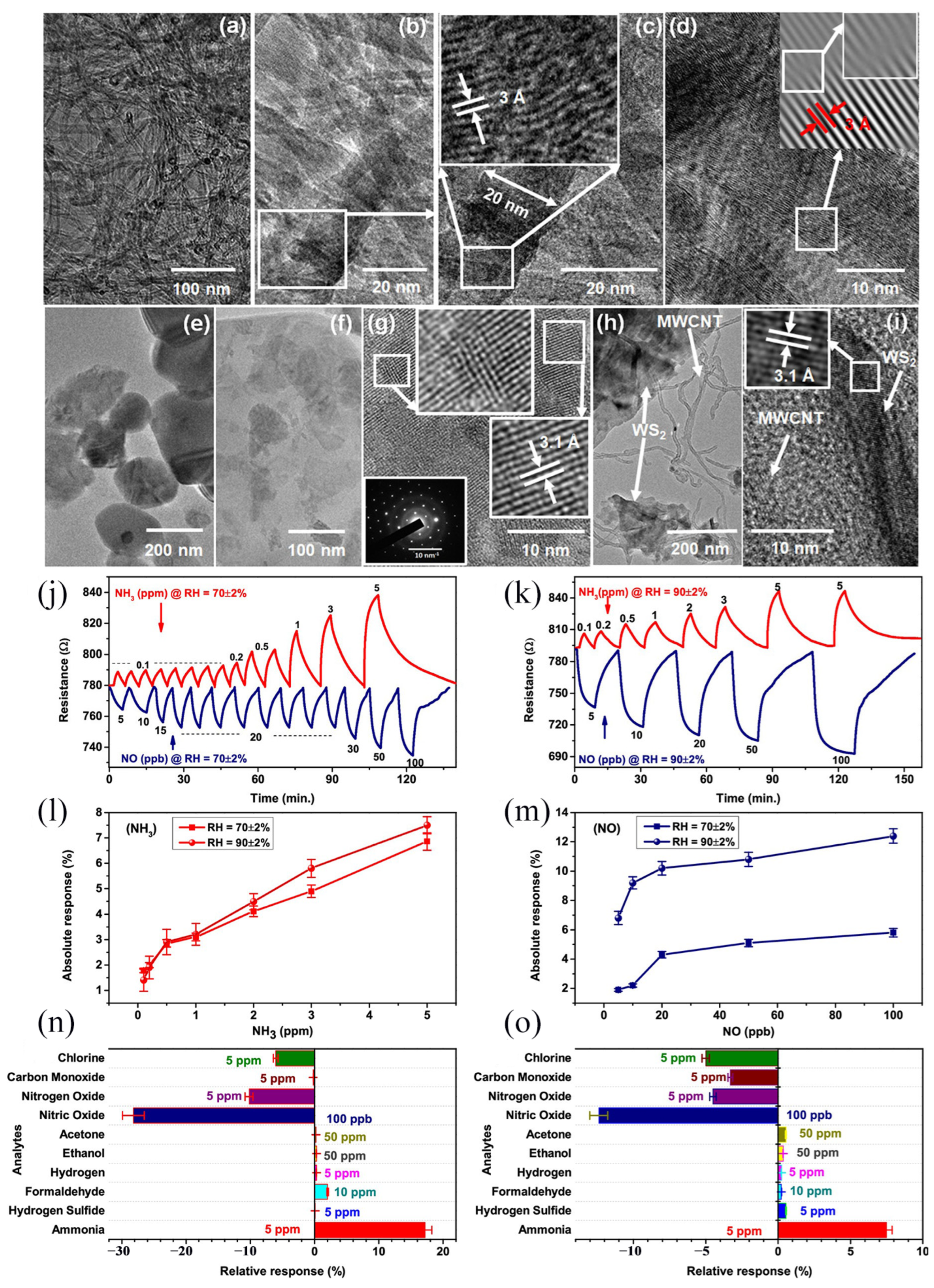
- Singh, S.; Saggu, I.S.; Chen, K.; Xuan, Z.; Swihart, M.T.; Sharma, S. Humidity-Tolerant Room-Temperature Selective Dual Sensing and Discrimination of NH3 and No Using a WS2/MWCNT Composite. ACS Appl. Mater. Interfaces 2022, 14, 40382–40395. [Google Scholar] [CrossRef] [PubMed]
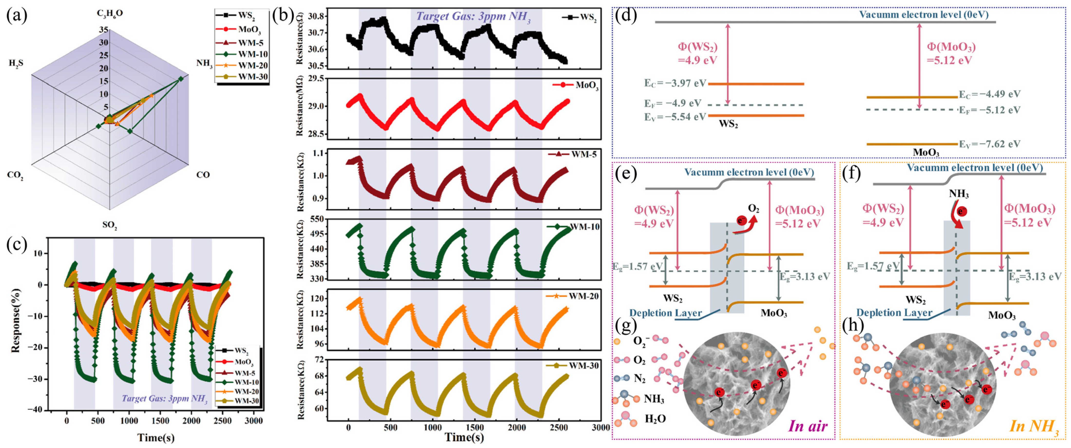
- Ou, Y.; Niu, W.; Zhou, Y.; Guo, Y.; Gao, C.; Wang, Y. Mesoporous WS2/MoO3 Hybrids for High-Performance Trace Ammonia Detection. ACS Appl. Mater. Interfaces 2022, 14, 39062–39071. [Google Scholar] [CrossRef] [PubMed]
- Kim, J.H.; Mirzaei, A.; Bang, J.H.; Kin, H.W.; Kim, S.S. Achievement of self-heated sensing of hazardous gases by WS2 (core)–SnO2 (shell) nanosheets. J. Hazard. Mater. 2021, 412, 125196. [Google Scholar] [CrossRef] [PubMed]
- Hao, L.; Liu, H.; Xu, H.; Dong, S.; Du, Y.; Wu, Y.; Zeng, H.; Zhu, J.; Liu, Y. Flexible Pd-WS2/Si heterojunction sensors for highly sensitive detection of hydrogen at room temperature. Sens. Actuators B 2019, 283, 740–748. [Google Scholar] [CrossRef]
- Ma, X.; Cai, X.; Yuan, M.; Qu, Y.; Tan, Y.; Chen, F. Self-powered and flexible gas sensor using defect-engineered WS2/G heterostructure. Sens. Actuators B 2022, 371, 132523. [Google Scholar] [CrossRef]
- Zhang, L.; Tan, Q.; Wang, Y.; Fan, Z.; Lin, L.; Zhang, W.; Xiong, J. Wirelessly powered multi-functional wearable humidity sensor based on RGO-WS2 heterojunctions. Sens. Actuators B 2021, 329, 9077. [Google Scholar] [CrossRef]
- Guo, Y.U.; Liu, B.; Duan, Z.; Yuan, Z.; Jiang, Y.; Tai, H. Batch fabrication of H2S sensors based on evaporated Pd/WO3 film with ppb-level detection limit. Mater. Chem. Phys. 2023, 302, 127768. [Google Scholar] [CrossRef]
- Kim, J.; Mirzaei, A.; Sakaguchi, I.; Hishita, S.; Ohsawa, T.; Suzuki, T.T.; Kim, S.S.; Saito, N. Decoration of Pt/Pd bimetallic nanoparticles on Ru-implanted WS2 nanosheets for acetone sensing studies. Appl. Surf. Sci. 2023, 641, 158478. [Google Scholar] [CrossRef]
- Zhao, W.; Zhao, Q.; Hao, H.; Lin, H.; Gao, W.; Yan, S. Hydrophobic modification of WO3/WS2 heterostructure for construction of humidity immune TEA sensors. Mater. Chem. Phys. 2023, 294, 126993. [Google Scholar] [CrossRef]
- Gao, Z.; Song, G.; Zhang, X.; Li, Q.; Yang, S.; Wang, T.; Li, Y.; Zhang, L.; Guo, L.; Fu, Y. A facile PDMS coating approach to room-temperature gas sensors with high humidity resistance and long-term stability. Sens. Actuators B 2020, 325, 128810. [Google Scholar] [CrossRef]
- Zhou, Y.; Wang, S.; Xin, S.; Sayin, s.; Yi, Z.; Li, Z.; Zaghloul, M. Layer-Dependent Sensing Performance of WS2-Based Gas Sensors. Nanomaterials 2024, 14, 235. [Google Scholar] [CrossRef] [PubMed]
- Li, M.Y.; Su, S.K.; Wong, H.S.P.; Li, L.J. How 2D semiconductors could extend Moore’s law. Nature 2019, 567, 169–170. [Google Scholar] [CrossRef] [PubMed]
- Bhimanapati, G.R.; Lin, Z.; Meunier, V.; Jung, Y.; Cha, J.; Das, S.; Xiao, D.; Son, Y.; Strano, M.S.; Cooper, V.R.; et al. Recent Advances in Two-Dimensional Materials beyond Graphene. ACS Nano 2015, 9, 11509–11539. [Google Scholar] [CrossRef] [PubMed]
- Liu, L.; Kumar, S.B.; Ouyang, Y.; Guo, J. Performance Limits of Monolayer Transition Metal Dichalcogenide Transistors. IEEE Trans. Electron Devices 2011, 58, 3042–3047. [Google Scholar] [CrossRef]
- Li, X.; Shi, X.; Marian, D.; Soriano, D.; Cusati, T.; Iannaccone, G.; Fiori, G.; Guo, Q.; Zhao, W.; Wu, Y. Rhombohedral-stacked bilayer transition metal dichalcogenides for high-performance atomically thin CMOS devices. Sci. Adv. 2023, 9, eade5706. [Google Scholar] [CrossRef] [PubMed]
- Shen, P.-C.; Su, C.; Lin, Y.; Chou, A.-S.; Cheng, C.-C.; Park, J.-H.; Chiu, M.-H.; Lu, A.-Y.; Tang, H.-L.; Tavakoli, M.M. Ultralow contact resistance between semimetal and monolayer semiconductors. Nature 2021, 593, 211–217. [Google Scholar] [CrossRef] [PubMed]
- Yeh, C.-H.; Cao, W.; Pal, A.; Parto, K.; Banerjee, K. Area-selective-CVD technology enabled top-gated and scalable 2D-heterojunction transistors with dynamically tunable Schottky barrier. In Proceedings of the IEEE International Electron Devices Meeting (IEDM), San Francisco, CA, USA, 7–11 December 2019. [Google Scholar]
- Brien, K.P.O.; Dorow, C.J.; Penumatcha, A.; Maxey, K.; Lee, S.; Naylor, C.H.; Hsiao, A.; Holybee, B.; Rogan, C.; Adams, D.; et al. Advancing 2D monolayer CMOS through contact. channel and interface engineering. In Proceedings of the IEEE International Electron Devices Meeting (IEDM), San Francisco, CA, USA, 11–16 December 2021. [Google Scholar]
- Dorow, C.J.; Brien, K.P.O.; Naylor, C.H.; Lee, S.; Penumatcha, A.; Hsiao, A.; Tronic, T.; Christenson, M.; Maxey, K.; Zhu, H.; et al. Advancing monolayer 2D NMOS and PMOS transistor integration from growth to van der Waals interface engineering for ultimate CMOS scaling. In Proceedings of the Symposium on VLSI Technology, Kyoto, Japan, 13–19 June 2021. [Google Scholar]
- Jin, L.; Koester, S.J. High-performance dual-gated single-layer WS2 MOSFETs with Bi Contacts. IEEE Electron Device Lett. 2022, 43, 639–642. [Google Scholar] [CrossRef]
- Smets, Q.; Schram, T.; Verreck, D.; Cott, D.; Groven, B.; Ahmed, Z.; Kaczer, B.; Mitard, J.; Wu, X.; Kundu, S.; et al. Scaling of double-gated WS2 FETs to sub-5nm physical gate length fabricated in a 300mm FAB. In Proceedings of the IEEE International Electron Devices Meeting (IEDM), San Francisco, CA, USA, 11–16 December 2021. [Google Scholar]
- Sebastian, A.; Pendurthi, R.; Choudhury, T.H.; Redwing, J.M.; Das, S. Benchmarking monolayer MoS2 and WS2 field-effect transistors. Nat. Commun. 2021, 12, 693. [Google Scholar] [CrossRef] [PubMed]
- Chubarov, M.; Choudhury, T.H.; Hickey, D.R.; Bachu, S.; Zhang, T.; Sebastian, A.; Bansal, A.; Zhu, H.; Trainor, N.; Das, S.; et al. Wafer-scale epitaxial growth of unidirectional WS2 monolayers on sapphire. ACS Nano 2021, 15, 2532–2541. [Google Scholar] [CrossRef] [PubMed]
- Yeh, C.-H.; Liang, Z.-Y.; Lin, Y.-C.; Ma, C.-H.; Chu, Y.-H.; Suenaga, K.; Chiu, P.-W. Scalable T-gate aligned Gr–WS2–Gr radio-frequency field-effect transistors. ACS Appl. Electron. Mater. 2020, 2, 3898–3905. [Google Scholar] [CrossRef]
- Pang, C.-S.; Wu, P.; Appenzeller, J.; Chen, Z. Thickness-dependent study of high-performance WS2-FETs with ultrascaled channel lengths. IEEE Trans. Electron Devices 2021, 68, 2123–2129. [Google Scholar] [CrossRef]
- Shi, X.; Li, X.; Guo, Q.; Zeng, M.; Wang, X.; Wu, Y. Ultrashort channel chemical vapor deposited bilayer WS2 field-effect transistors. Appl. Phys. Rev. 2023, 10, 011405. [Google Scholar] [CrossRef]
- Shi, X.; Li, X.; Guo, Q.; Gao, H.; Zeng, M.; Han, Y.; Yan, S.; Wu, Y. Improved Self-Heating in Short-Channel Monolayer WS2 Transistors with High-Thermal Conductivity BeO Dielectrics. Nano Lett. 2022, 22, 7667–7673. [Google Scholar] [CrossRef] [PubMed]
- Hou, J.; Ke, C.; Chen, J.; Sun, B.; Xia, Y.; Li, X.; Chen, T.; Wu, Y.; Wu, Z.; Kang, J. Reduced turn-on voltage and boosted mobility in monolayer WS2 transistors by mild Ar+ plasma treatment. ACS Apl. Mater. Interfaces 2020, 12, 19635–19642. [Google Scholar] [CrossRef]
- Liu, M.; Wei, S.; Shahi, S.; Jaiswal, H.N.; Paletti, P.; Fathipour, S.; Remškar, M.; Jiao, J.; Hwang, W.; Yao, F.; et al. Enhanced carrier transport by transition metal doping in WS2 field effect transistors. Nanoscale 2020, 12, 17253–17264. [Google Scholar] [CrossRef] [PubMed]
- Jiang, J.; Zhang, Q.; Wang, A.; Zhang, Y.; Meng, F.; Zhang, C.; Feng, X.; Feng, Y.; Gu, L.; Liu, H.; et al. A facile and effective method for patching sulfur vacancies of WS2 via nitrogen plasma treatment. Small 2019, 15, 1901791. [Google Scholar] [CrossRef] [PubMed]
- Zheng, S.; Lu, H.; Liu, H.; Liu, D.; Robertson, J. Insertion of an ultrathin Al2O3 interfacial layer for Schottky barrier height reduction in WS2 field-effect transistors. Nanoscale 2019, 11, 4811–4821. [Google Scholar] [CrossRef] [PubMed]
- Phan, N.A.N.; Noh, H.; Kim, J.; Kim, Y.; Kim, H.; Whang, D.; Aoki, N.; Watanabe, K.; Taniguchi, T.; Kim, G.H. Enhanced Performance of WS2 Field-Effect Transistor through Mono and Bilayer h-BN Tunneling Contacts. Small 2022, 18, 2105753. [Google Scholar] [CrossRef] [PubMed]
- Acar, M.; Mobtakeri, S.; Efeoğlu, H.; Ertuğrul, M.; Gür, E. Single-step, large-area, variable thickness sputtered WS2 film-based field effect transistors. Ceram. Int. 2020, 46, 26854–26860. [Google Scholar] [CrossRef]
- Xie, J.; Meng, G.; Chen, B.; Li, Z.; Yin, Z.; Cheng, Y. Vapor–Liquid–Solid Growth of Morphology-Tailorable WS2 toward P-Type Monolayer Field-Effect Transistors. ACS Appl. Mater. Interfaces 2022, 14, 45716–45724. [Google Scholar] [CrossRef] [PubMed]
- Liang, J.; Zhang, L.; Li, X.; Pan, B.; Luo, T.; Liu, N.; Zou, C.; Yang, Y.; Huang, S. Electron Transport Properties of WS2 Field-Effect Transistors Modulated by Electron Beam Irradiation Under Gate Voltage. IEEE Electron Device Lett. 2019, 40, 1542–1545. [Google Scholar] [CrossRef]
- Chen, Y.; Jiang, Y.; Yi, C.; Liu, H.; Chen, S.; Sun, X.; Ma, C.; Li, D.; He, C.; Luo, Z. Efficient control of emission and carrier polarity in WS2 monolayer by indium doping. Sci. China Mater. 2021, 64, 1449–1456. [Google Scholar] [CrossRef]
- Luo, Z.D.; Xia, X.; Yang, M.M.; Wilson, N.R.; Gruverman, A.; Alexe, M. Artificial optoelectronic synapses based on ferroelectric field-effect enabled 2D transition metal dichalcogenide memristive transistors. ACS Nano 2019, 14, 746–754. [Google Scholar] [CrossRef] [PubMed]
- Chen, L.; Wang, L.; Peng, Y.; Feng, X.; Sarkar, S.; Li, S.; Li, B.; Liu, L.; Han, K.; Gong, X.; et al. A van der Waals synaptic transistor based on ferroelectric Hf0. 5Zr0. 5O2 and 2D tungsten disulfide. Adv. Electron. Mater. 2020, 6, 2000057. [Google Scholar] [CrossRef]
- Zhang, Y.; Wang, L.; Yang, M.; Lin, D.; Wang, B.; Zhang, N.; Jiang, Z.; Liu, M.; Zhu, Z.; Hu, H. Multiposition Controllable Gate WS2/MoS2 Heterojunction Phototransistor and Its Applications in Optoelectronic Logic Operation and Emulation of Neurotransmission. Adv. Opt. Mater. 2020, 10, 2200197. [Google Scholar] [CrossRef]
- Liu, L.; Li, T.; Ma, L.; Li, W.; Gao, S.; Sun, W.; Wang, X. Uniform nucleation and epitaxy of bilayer molybdenum disulfide on sapphire. Nature 2022, 605, 69–75. [Google Scholar] [CrossRef] [PubMed]
- Kim, J.; An, G.H.; Bang, S.; Park, D.G.; Kim, D.; Lee, J.W. Comparative analysis of Schottky barriers for heterogeneous defect domains in monolayer WS2 field-effect transistors. Appl. Surf. Sci. 2022, 604, 154600. [Google Scholar] [CrossRef]
- Bai, Z.; Luo, Q.; Li, M.; Peng, G.; Zhu, Z.; Novoselov, K. Highly tunable carrier tunneling in vertical graphene–WS2–graphene van der Waals heterostructures. ACS Nano 2022, 16, 7880–7889. [Google Scholar] [CrossRef] [PubMed]
- Chung, C.H.; Chen, H.R.; Ho, M.J.; Lin, C.Y. WS2 transistors with sulfur atoms being replaced at the interface: First-principles quantum-transport study. ACS Omega 2023, 8, 10419–10425. [Google Scholar] [CrossRef] [PubMed]
- Zhang, S.; Chuang, H.J.; Le, S.T.; Richter, C.A.; McCreary, K.M.; Jonker, B.T.; Hacker, C.A. Control of the Schottky barrier height in monolayer WS2 FETs using molecular doping. AIP Adv. 2022, 12, 085222. [Google Scholar] [CrossRef]
- Zhang, Y.; Zhao, F.; Wang, Y.; Wang, Y.; Feng, Y.; Feng, W. Tapping the Performance of a Tungsten Disulfide Field-Effect Transistor with Deep Structure Optimization and Theoretical Simulation. ACS Appl. Electron. Mater. 2023, 5, 3384–3393. [Google Scholar] [CrossRef]
- Ge, S.; Sang, D.; Zou, L.; Yao, Y.; Zhou, C.; Fu, H.; Xi, H.; Fan, J.; Meng, L.; Wang, C. A Review on the Progress of Optoelectronic Devices Based on TiO2 Thin Films and Nanomaterials. Nanomaterials 2023, 13, 1141. [Google Scholar] [CrossRef] [PubMed]
- Wang, Z.; Zhang, X.; Wu, D.; Guo, J.; Zhao, Z.; Shi, Z.; Tian, Y.; Huang, X.; Li, X. Construction of mixed-dimensional WS2/Si heterojunctions for high-performance infrared photodetection and imaging applications. J. Mater. Chem. C 2020, 8, 6877–6882. [Google Scholar] [CrossRef]
- Jang, C.W.; Choi, S.H. Self-powered semitransparent/flexible doped-graphene/WS2 vertical-heterostructure photodetectors. J. Alloys Compd. 2022, 901, 163685. [Google Scholar] [CrossRef]
- Kim, B.H.; Yoon, H.; Kwon, S.H.; Kim, D.W.; Yoon, Y.J. Direct WS2 photodetector fabrication on a flexible substrate. Vacuum 2021, 184, 109950. [Google Scholar] [CrossRef]
- Wu, D.; Guo, J.; Wang, C.; Ren, X.; Chen, Y.; Lin, P.; Zeng, L.; Shi, Z.; Li, X.J.; Shan, C.X.; et al. Ultrabroadband and high-detectivity photodetector based on WS2/Ge heterojunction through defect engineering and interface passivation. ACS Nano 2021, 15, 10119–10129. [Google Scholar] [CrossRef] [PubMed]
- Jia, C.; Huang, X.; Wu, D.; Tian, Y.; Guo, J.; Zhao, Z.; Shi, Z.; Tian, Y.; Jie, J.; Li, X. An ultrasensitive self-driven broadband photodetector based on a 2D-WS2/GaAs type-II Zener heterojunction. Nanoscale 2020, 12, 4435–4444. [Google Scholar] [CrossRef]
- Wu, D.; Guo, C.; Wang, Z.; Ren, X.; Tian, Y.; Shi, Z.; Lin, P.; Tian, Y.; Chen, Y.; Li, X. A defect-induced broadband photodetector based on WS2/pyramid Si 2D/3D mixed-dimensional heterojunction with a light confinement effect. Nanoscale 2021, 13, 13550–13557. [Google Scholar] [CrossRef] [PubMed]
- Kanade, C.K.; Seok, H.; Kanade, V.K.; Aydin, K.; Kim, H.; Mitta, S.B.; Yoo, W.J.; Kim, T. Low-temperature and large-scale production of a transition metal sulfide vertical heterostructure and its application for photodetectors. ACS Appl. Mater. Interfaces 2021, 13, 8710–8717. [Google Scholar] [CrossRef] [PubMed]
- Chowdhury, R.K.; Sinha, T.K.; Katiyar, A.K.; Ray, S.K. Synergistic effect of polymer encapsulated silver nanoparticle doped WS2 sheets for plasmon enhanced 2D/3D heterojunction photodetectors. Nanoscale 2017, 9, 15591–15597. [Google Scholar] [CrossRef] [PubMed]
- Nguyen, T.T.; Patel, M.; Ban, D.K.; Kim, J. Vertically trigonal WS2 layer embedded heterostructure for enhanced ultraviolet–visible photodetector. J. Alloys Compd. 2018, 768, 143–149. [Google Scholar] [CrossRef]
- Lukman, S.; Ding, L.; Xu, L.; Tao, Y.; Jensen, A.C.R.; Zhang, G.; Wu, Q.Y.S.; Yang, M.; Luo, S.; Hsu, C.; et al. High oscillator strength interlayer excitons in two-dimensional heterostructures for mid-infrared photodetection. Nat. Nanotechnol. 2020, 15, 675–682. [Google Scholar] [CrossRef] [PubMed]
- Zheng, D.; Dong, X.; Lu, J.; Niu, Y.; Wang, H. High-Sensitivity Infrared Photoelectric Detection Based on WS2/Si Structure Tuned by Ferroelectrics. Small 2022, 18, 2105188. [Google Scholar] [CrossRef]
- Ozdemir, O.; Ramiro, I.; Gupta, S.; Konstantatos, G. High sensitivity hybrid PbS CQD-TMDC photodetectors up to 2 μm. Acs Photon. 2019, 6, 2381–2386. [Google Scholar] [CrossRef]
- Zhao, Z.; Wu, D.; Guo, J.; Wu, E.; Jia, C.; Shi, Z.; Tian, Y.; Li, X.; Tian, Y. Synthesis of large-area 2D WS2 films and fabrication of a heterostructure for self-powered ultraviolet photodetection and imaging applications. J. Mater. Chem. C 2019, 7, 12121–12126. [Google Scholar] [CrossRef]
- Shelke, N.T.; Karche, B.R. Hydrothermal synthesis of WS2/RGO sheet and their application in UV photodetector. J. Alloys and Compd. 2015, 653, 298–303. [Google Scholar] [CrossRef]
- Wang, F.; Li, Q.; Wang, P.; Xia, H.; Wang, Z.; Wang, Y.; Luo, M.; Chen, L.; Chen, F.; Miao, J.; et al. High efficiency and fast van der Waals hetero-photodiodes with a unilateral depletion region. Nat. Commun. 2019, 10, 4663. [Google Scholar]
- Luo, Z.; Xu, H.; Gao, W.; Yang, M.; He, Y.; Huang, Z.; Yao, J.; Zhang, M.; Dong, H.; Zhao, Y. High-Performance and Polarization-Sensitive Imaging Photodetector Based on WS2/Te Tunneling Heterostructure. Small 2023, 19, 2207615. [Google Scholar] [CrossRef] [PubMed]
- Fang, F.; Wan, Y.; Li, H.; Fang, S.; Huang, F.; Zhou, B.; Jiang, K.; Tung, V.; Li, L.; Shi, Y. Two-dimensional Cs2AgBiBr6/WS2 heterostructure-based photodetector with boosted detectivity via interfacial engineering. ACS Nano 2022, 16, 3985–3993. [Google Scholar] [CrossRef]
- Chekke, T.; Narzary, R.; Ngadong, S.; Satpati, B.; Bayan, S.; Das, U. Au decorated ultrathin WS2-based single-electrode triboelectric nanogenerator for flexible self-powered photodetector. Sens. Actuators A 2023, 349, 114076. [Google Scholar] [CrossRef]
- Zhang, X.; Dong, Q.; Li, Z.; Liu, R.; Zhao, T.; Lin, T.; Li, Q.; Liu, B. Significant pressure-induced enhancement of photoelectric properties of WS2 in the near-infrared region. Mater. Res. Lett. 2022, 10, 547–555. [Google Scholar] [CrossRef]
- Singh, A.; Chauhan, P. WS2–polyaniline nanohybrid materials for high-external quantum efficiency photoelectric devices utilized in flexible electronics. ACS Appl. Opt. Mater. 2023, 2, 28–40. [Google Scholar] [CrossRef]
- Grillo, A.; Passacantando, M.; Zak, A.; Pelella, A.; Bartolomeo, A.D. WS2 nanotubes: Electrical conduction and field emission under electron irradiation and mechanical stress. Small 2020, 16, 2002880. [Google Scholar] [CrossRef] [PubMed]
- Di Bartolomeo, A.; Giubileo, F.; Iemmo, L.; Romeo, F.; Russo, S.; Unal, S.; Passacantando, M.; Grossi, V.; Cucolo, A.M. Giuseppe Leakage and field emission in side-gate graphene field effect transistors. Appl. Phys. Lett. 2016, 109, 023510. [Google Scholar] [CrossRef]
- Loh Tamie, A.J.; Ying, J.O.; Daniel, H.C. WS2 nano-petals and nano-bristles supported on carbon nanotubes for electron emission applications. Sci. Rep. 2019, 9, 3672. [Google Scholar] [PubMed]
- Siao, M.D.; Gandhi, A.C.; Sahoo, A.K.; Wu, Y.C.; Syu, H.K.; Tsai, M.Y.; Tsai, T.H.; Tang, Y.C.; Lin, Y.F.; Liu, R.S.; et al. WSe2/WS2 Heterobilayer Nonvolatile Memory Device with Boosted Charge Retention. ACS Appl. Mater. Interface 2022, 14, 3467–3475. [Google Scholar] [CrossRef] [PubMed]
- Zhou, Y.; Ning, J.; Shen, X.; Guo, H.; Zhang, C.; Dong, J.; Lu, W.; Feng, X.; Hao, Y. An Ultrafast Quasi-Non-Volatile Semi-Floating Gate Memory with Low-Power Optoelectronic Memory Application. Adv. Electron. Mater. 2021, 7, 2100564. [Google Scholar] [CrossRef]
- Das, U.; Bhattacharjee, S.; Mahato, B.; Prajapat, M.; Sarkar, P.; Roy, A. Uniform, large-scale growth of WS2 nanodomains via CVD technique for stable non-volatile RRAM application. Mater. Sci. Semicond. Process. 2020, 107, 104837. [Google Scholar] [CrossRef]
- Ye, T.; Li, Y.; Li, J.; Shen, H.; Ren, J.; Ning, C.Z.; Li, D. Nonvolatile electrical switching of optical and valleytronic properties of interlayer excitons. Light Sci. Appl. 2022, 11, 23. [Google Scholar] [CrossRef] [PubMed]
- Siao, M.D.; Lin, Y.C.; He, T.; Tsai, M.Y.; Lee, K.Y.; Chang, S.Y.; Lin, K.; Lin, Y.F.; Chou, M.Y.; Suenaga, K.; et al. Embedment of Multiple Transition Metal Impurities into WS2 Monolayer for Bandstructure Modulation. Small 2021, 17, 2007171. [Google Scholar] [CrossRef]
- Zhu, X.; He, L.; Yang, Y.; Zhang, K.; Zhu, H.; Chen, L.; Sun, Q. Multibit non-volatile memory based on WS2 transistor with engineered gate stack. AIP Adv. 2020, 10, 125124. [Google Scholar] [CrossRef]
- Shen, H.; Ren, J.; Hu, J. Low-Power Logic-in-Memory Complementary Inverter Based on p-WSe2 and n-WS2. Adv. Electron. Mater. 2022, 8, 2200768. [Google Scholar] [CrossRef]
- Khalid, A.; Ahmad, P.; Saeedi, A.M.; Liaqat, I.; EL-Gawaad, N.S.A.; Idris, S.A.; Alanazi, A.M.; Alsehli, A.H.; Alsowayigh, M.M.; Alderhami, S.A. Few layer chemical vapor deposited two dimensional WS2 for low voltage resistive switching application. Microelectron. Eng. 2023, 281, 112083. [Google Scholar] [CrossRef]
- Tong, L.; Duan, X.; Song, L.; Liu, T.; Ye, L.; Huang, X.; Cheng, G.J. Artificial control of in-plane anisotropic photoelectricity in monolayer MoS2. Appl. Mater. Today 2019, 15, 203–211. [Google Scholar] [CrossRef]
- Bharathi, P.; Harish, S.; Mathankumar, G.; Mohan, M.K.; Archana, J.; Kamalakannan, S.; Navaneethan, M. Solution processed edge activated Ni-MoS2 nanosheets for highly sensitive room temperature NO2 gas sensor applications. Appl. Surf. Sci. 2022, 600, 154086. [Google Scholar] [CrossRef]
- Zou, L.R.; Sang, D.D.; Yao, Y.; Wang, X.T.; Zheng, Y.Y.; Wang, N.Z.; Wang, C.; Wang, Q.L. Research progress of optoelectronic devices based on two-dimensional MoS2 materials. Rare Met. 2023, 42, 17–38. [Google Scholar] [CrossRef]
- Li, P.; Yuan, K.; Lin, D.Y.; Wang, T.; Du, W.; Wei, Z.; Dai, L. p-MoS2/n-InSe van der Waals heterojunctions and their applications in all-2D optoelectronic devices. RSC Adv. 2019, 9, 35039–35044. [Google Scholar] [CrossRef] [PubMed]
- Rai, S.; Singh, V.K.; Pendurthi, R.; Nasr, J.R.; Das, S.; Srivastava, A. Unveiling the electrical and photo-physical properties of intrinsic n-type 2D WSe2 for high performance field-effect transistors. J. Appl. Phys. 2022, 131, 094301. [Google Scholar] [CrossRef]
- Islam, Z.; Kozhakhmetov, A.; Robinson, J.; Haque, A. Enhancement of WSe2 FET Performance Using Low-Temperature Annealing. J. Electron. Mater. 2020, 49, 3770–3779. [Google Scholar] [CrossRef]
- Di Bartolomeo, A.; Urban, F.; Passacantando, M.; McEvoy, N.; Peters, L.; Iemmo, L.; Giubileo, F. A WSe2 vertical field emission transistor. Nanoscale 2019, 11, 1538–1548. [Google Scholar] [CrossRef] [PubMed]
- Lin, Y.; Wang, X.; Lin, Z.; Li, X.; Zhong, Z.; Botcha, V.D.; Liu, X. Optimization engineering of ReS2 photodetector by enhanced light scattering effects based on patterned substrates. J. Alloys Compd. 2023, 966, 171538. [Google Scholar] [CrossRef]
- Du, X.; Liu, T.; Wang, J.; Wang, P.; Wang, L.; Zheng, Y.; Chen, W. Anomalous broadband spectrum photodetection in 2D rhenium disulfide transistor. Adv. Opt. Mater. 2019, 7, 1901115. [Google Scholar]
- Zhang, Y.; Feng, Q.; Hao, R.; Zhang, M. Fabrication of Large-Area Short-Wave Infrared Array Photodetectors under High Operating Temperature by High Quality PtS2 Continuous Films. Electronics 2022, 11, 838. [Google Scholar] [CrossRef]
- Liu, J.; Xu, H.; Yan, J.; Huang, J.; Song, Y.; Deng, J.; Li, H. Efficient photocatalytic hydrogen evolution mediated by defect-rich 1T-PtS2 atomic layer nanosheet modified mesoporous graphitic carbon nitride. J. Mater. Chem. A 2019, 7, 18906–18914. [Google Scholar] [CrossRef]


| Materials | WS2 Morphology | Synthesis Route | Application | Ref. |
|---|---|---|---|---|
| Ion-gel/Au/Ni/WS2/PEN | Monolayer | CVD | Polarized LED | [37] |
| ITO/PEDOT:PSS/poly-TPD/WS2/ZnO/Al | Monolayer | MOCVD | OLED | [38] |
| Au/WS2/Si/SiO2 | Monolayer | Mechanical exfoliation | ACLED | [40] |
| Ion-gel/Au/WS2(1−x)Se2x | Monolayer | CVD | Wavelength adjustable LED | [41] |
| Materials | WS2 Morphology | Synthesis Route | Application | Ref. |
|---|---|---|---|---|
| WS2/Ni-In2O3 | Nanosheets | Hydrothermal method | Gas Sensor | [47] |
| WS2/ZnO | Few layers | Laser lift-off | Gas Sensor | [48] |
| WS2/WO3 | Nanosheets | In situ oxidation method | Gas Sensor | [49] |
| WS2/SnO2 | Nanosheets | Hydrothermal method | Gas Sensor | [51] |
| Pd-WS2/Si | Few layers | Sputters | Flexible sensors | [61] |
| WS2/Graphene | Monolayer | CVD | Flexible sensors | [62] |
| RGO/WS2 | Few layers | Hydrothermal method | Humidity sensor | [63] |
| Materials | WS2 Morphology | Synthesis Route | Application | Ref. |
|---|---|---|---|---|
| WS2 | Nanosheets | Mechanical exfoliation | Dual door control FETs | [82] |
| WS2 | Bilayer | CVD | MOSFET | [83] |
| WS2/Al2O3 | Nanosheets | Mechanical exfoliation | MIS contact FET | [88] |
| WS2 | Monolayer | VLS | P-type channel FETs | [91] |
| HZO/WS2 | Nanosheets | Mechanical exfoliation | Synaptic transistors | [95] |
| WS2/MoS2 | Few layers | CVD and mechanical exfoliation | Phototransistors | [96] |
| Materials | WS2 Morphology | Synthesis Route | Application | Ref. |
|---|---|---|---|---|
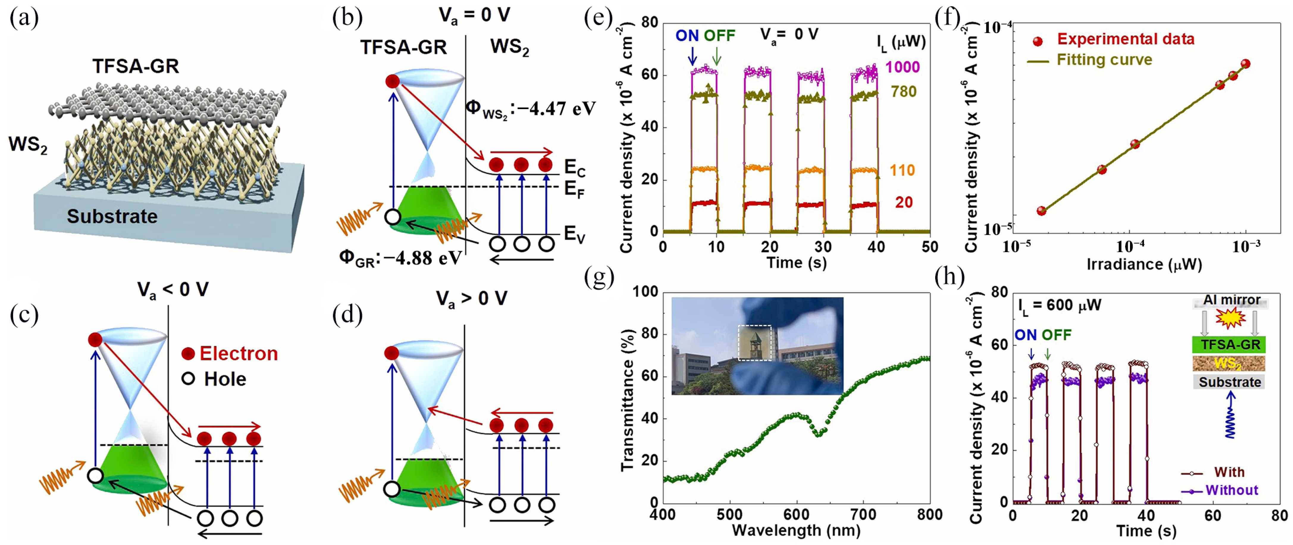
| TFSA-GR/WS2 | Few layers | CVD | Flexible photodetectors | [105] |
| WS2 | Few layers | RF magnetron sputtering and electron-beam irradiation | Flexible photodetectors | [106] |
| WS2/GaAs | Few layers | Two-step thermal decomposition method | Wide spectrum photodetectors | [108] |
| WS2/PbS | Nanosheets | Mechanical exfoliation | Infrared photodetectors | [115] |
| RGO/WS2 | Nanosheets | Hydrothermal reaction | Ultraviolet photodetectors | [117] |
| Materials | WS2 Morphology | Synthesis Route | Application | Ref. |
|---|---|---|---|---|
| WS2 | Few layers | EBVD | Field emission devices | [14] |
| WS2/Si | Nanotubes | High-temperature solid-gas synthetic | Field emission devices | [124] |
| WS2/CNTs | Few layers | RF Magnetron Sputtering | Field emission devices | [126] |
| Materials | WS2 Morphology | Synthesis Route | Application | Ref. |
|---|---|---|---|---|
| WS2/hBN/Graphene | Nanosheets | Mechanical exfoliation | Non-volatile memory devices | [128] |
| Al/WS2/Pt/Ti | Few layers | CVD | Non-volatile memory devices | [129] |
| WS2/WSe2 | Monolayer | Mechanical exfoliation | Non-volatile memory devices | [130] |
| MED WS2 | Monolayer | Monolayer | Non-volatile memory devices | [131] |
| ITO/Al2O3/Ta2O5/Al2O3/WS2 | Few layers | Mechanical exfoliation | Non-volatile memory devices | [132] |
Disclaimer/Publisher’s Note: The statements, opinions and data contained in all publications are solely those of the individual author(s) and contributor(s) and not of MDPI and/or the editor(s). MDPI and/or the editor(s) disclaim responsibility for any injury to people or property resulting from any ideas, methods, instructions or products referred to in the content. |
© 2024 by the authors. Licensee MDPI, Basel, Switzerland. This article is an open access article distributed under the terms and conditions of the Creative Commons Attribution (CC BY) license (https://creativecommons.org/licenses/by/4.0/).
Share and Cite
Li, C.; Sang, D.; Ge, S.; Zou, L.; Wang, Q. Recent Excellent Optoelectronic Applications Based on Two-Dimensional WS2 Nanomaterials: A Review. Molecules 2024, 29, 3341. https://doi.org/10.3390/molecules29143341
Li C, Sang D, Ge S, Zou L, Wang Q. Recent Excellent Optoelectronic Applications Based on Two-Dimensional WS2 Nanomaterials: A Review. Molecules. 2024; 29(14):3341. https://doi.org/10.3390/molecules29143341
Chicago/Turabian StyleLi, Changxing, Dandan Sang, Shunhao Ge, Liangrui Zou, and Qinglin Wang. 2024. "Recent Excellent Optoelectronic Applications Based on Two-Dimensional WS2 Nanomaterials: A Review" Molecules 29, no. 14: 3341. https://doi.org/10.3390/molecules29143341