
Copper(I) Iodide Thin Films: Deposition Methods and Hole-Transporting Performance


Abstract
:
1. Introduction
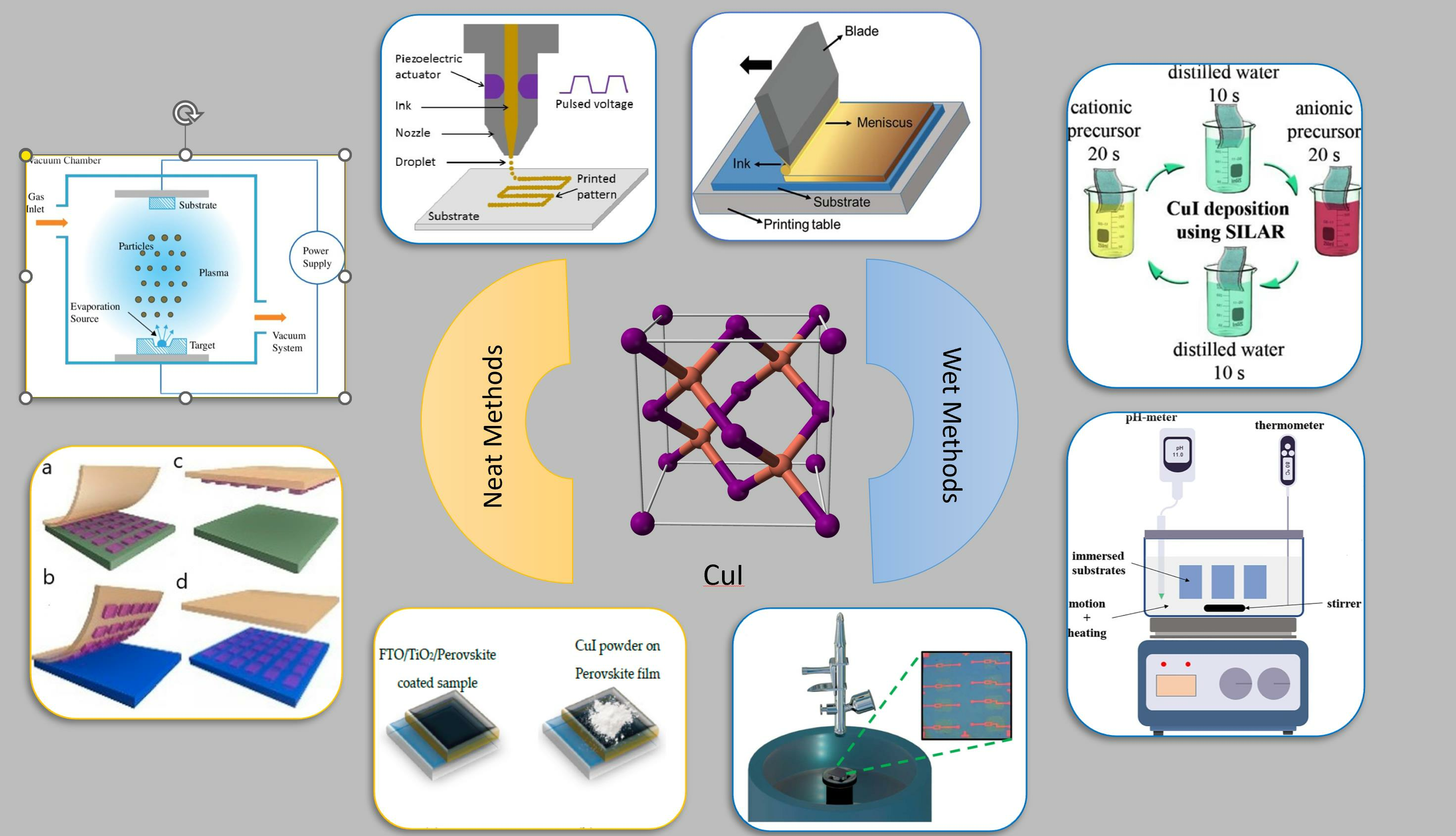
2. Deposition Methods of Copper Iodide Thin Film
2.1. Solution-Processed Methods
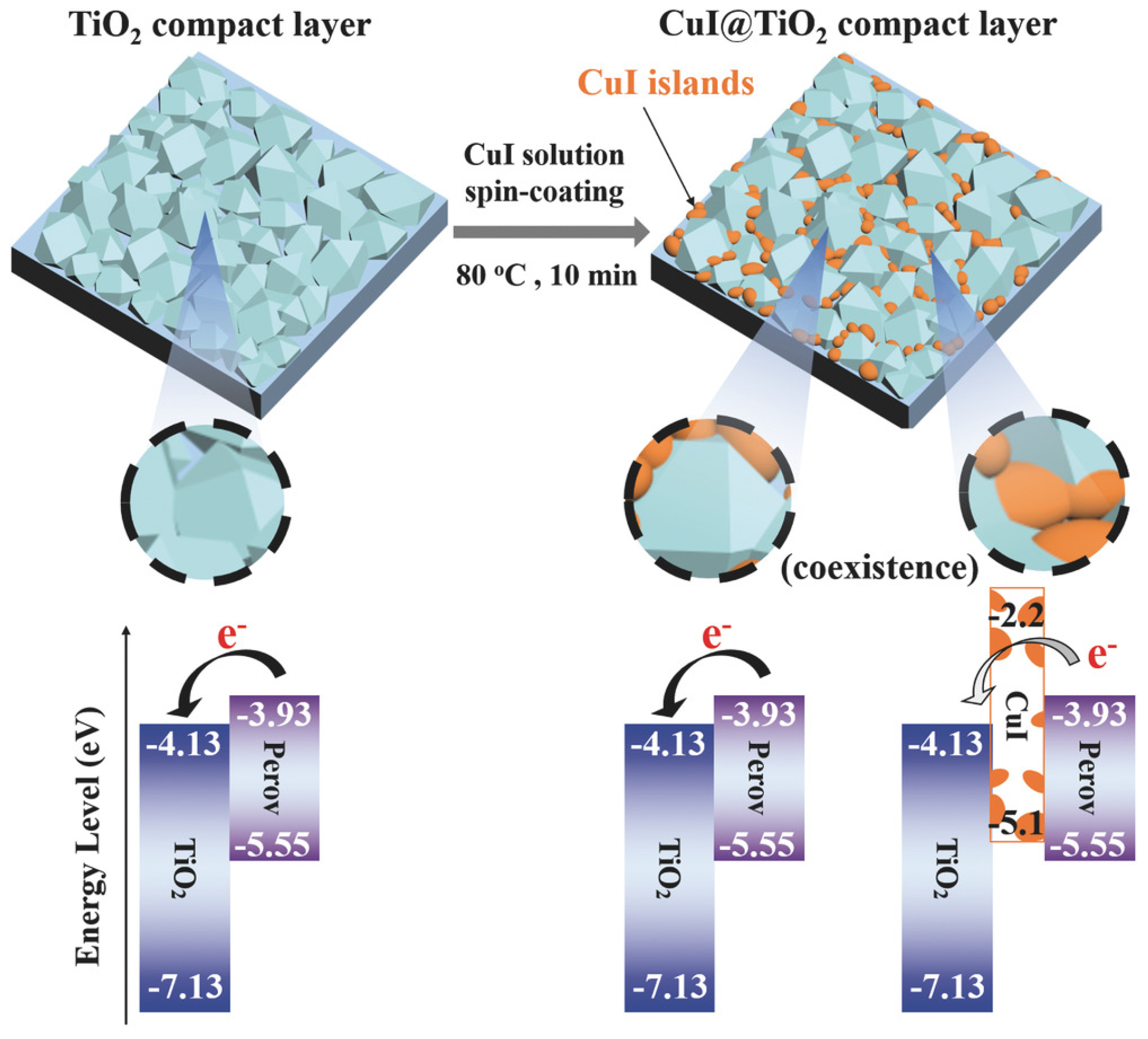
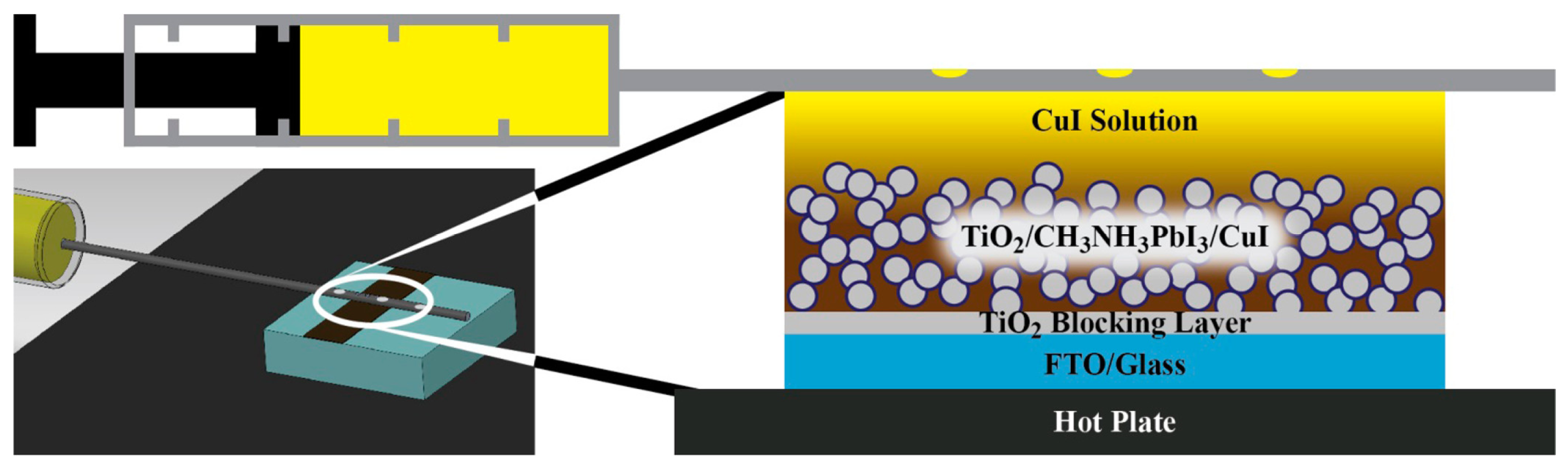
2.1.1. Spin Coating
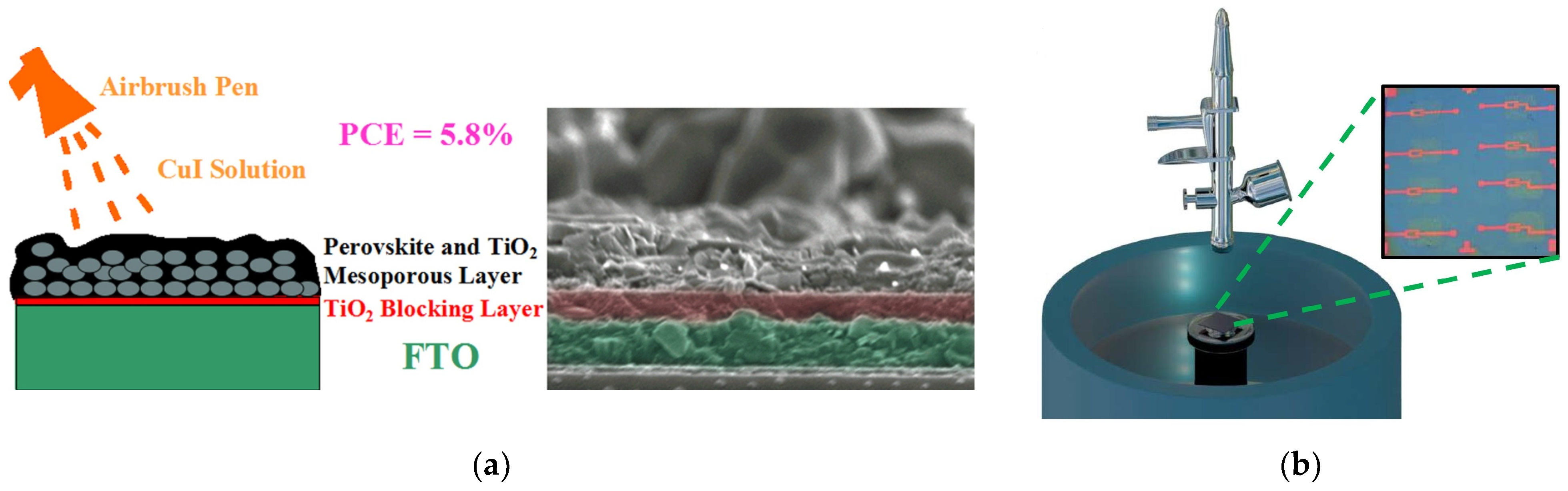
2.1.2. Spray Coating

2.1.3. Spray–Spin Coating
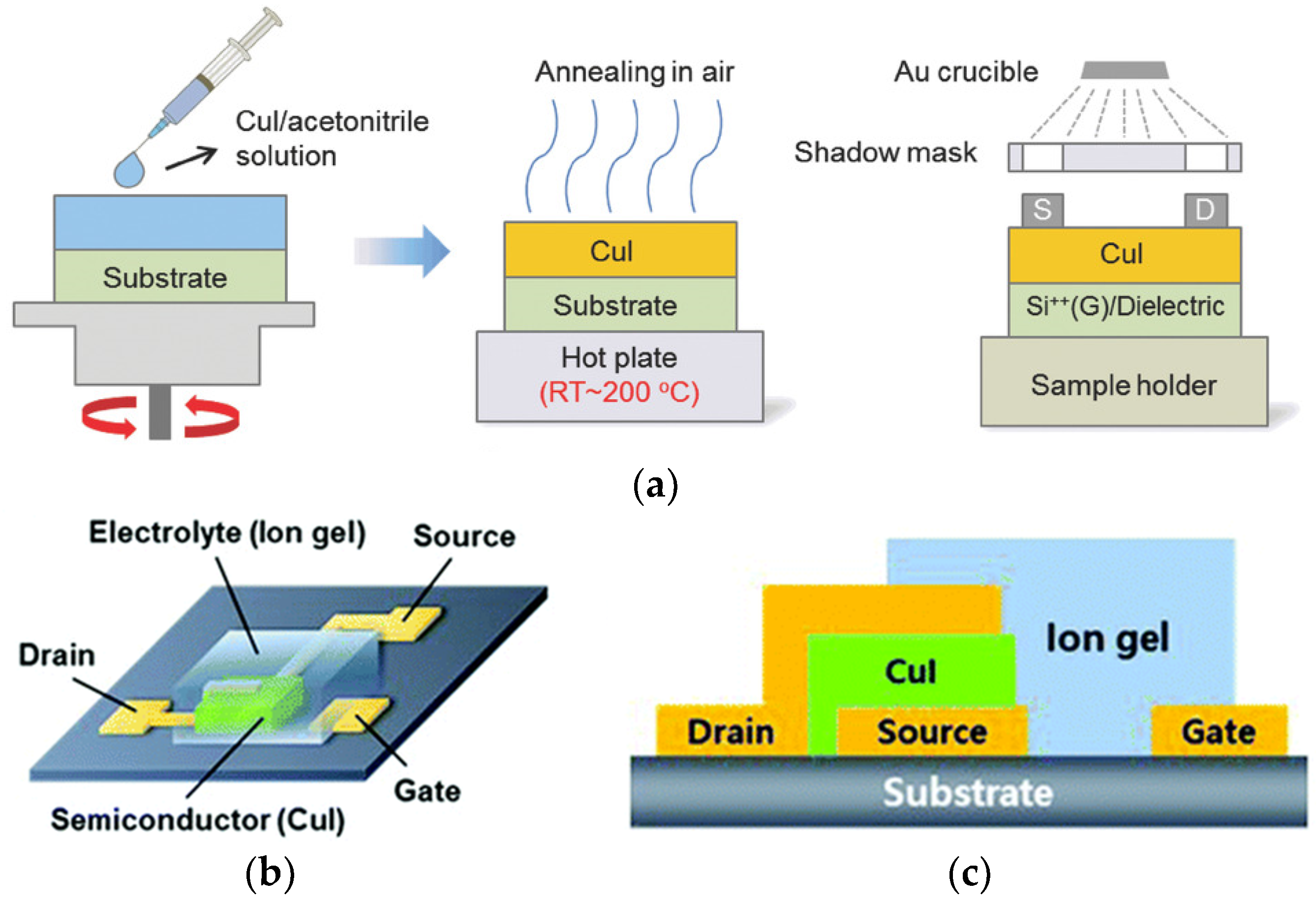
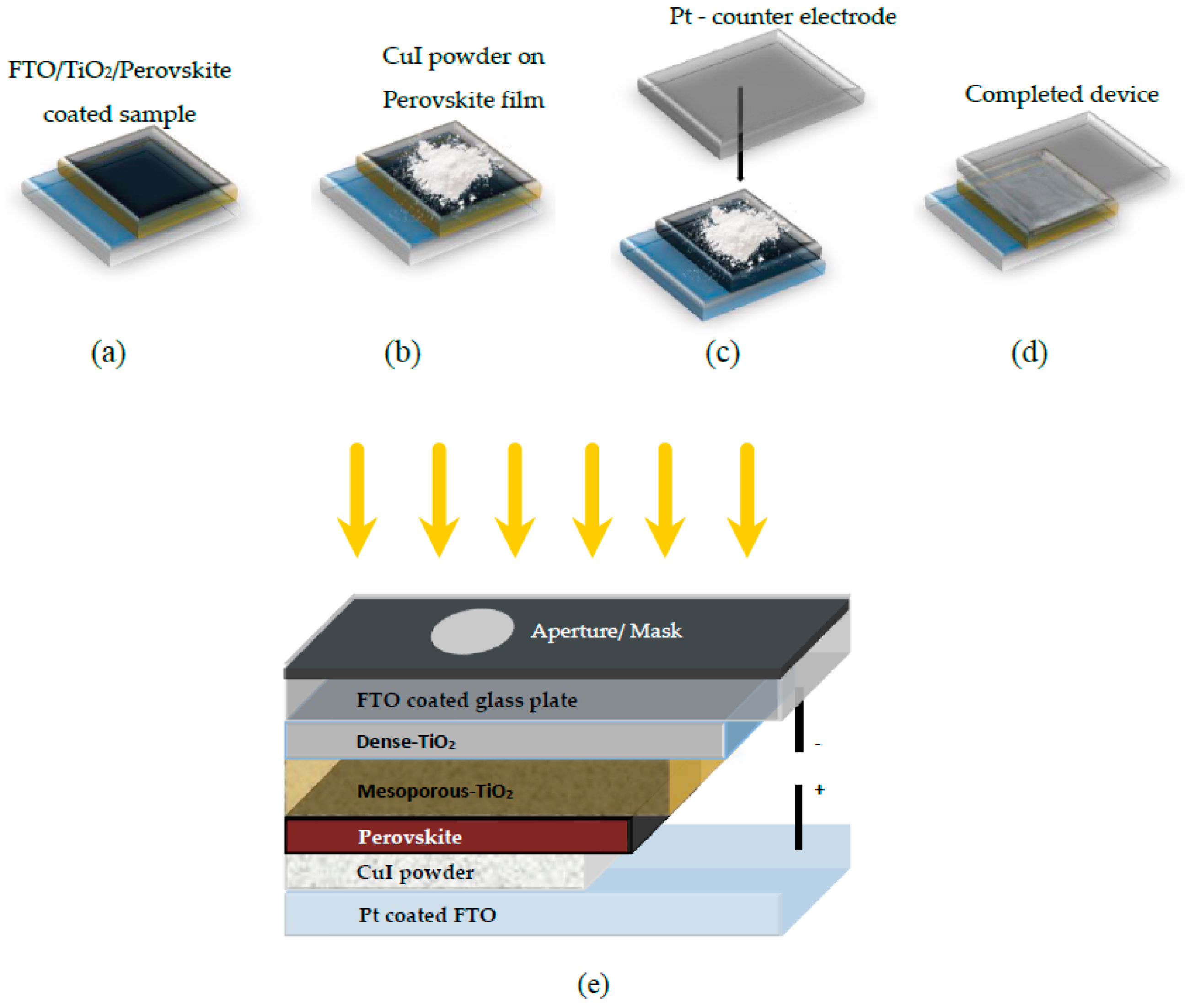
2.1.4. Drop Casting
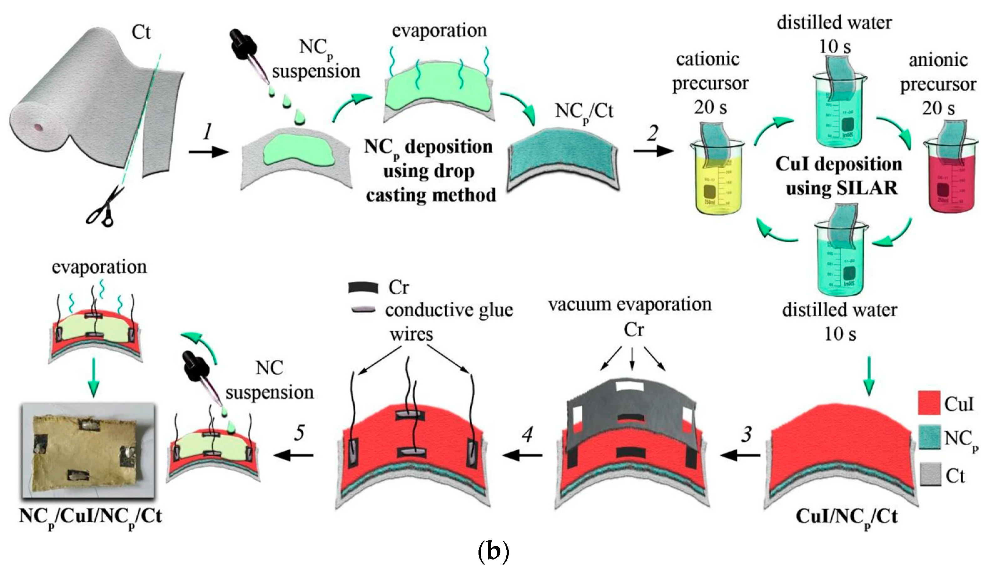
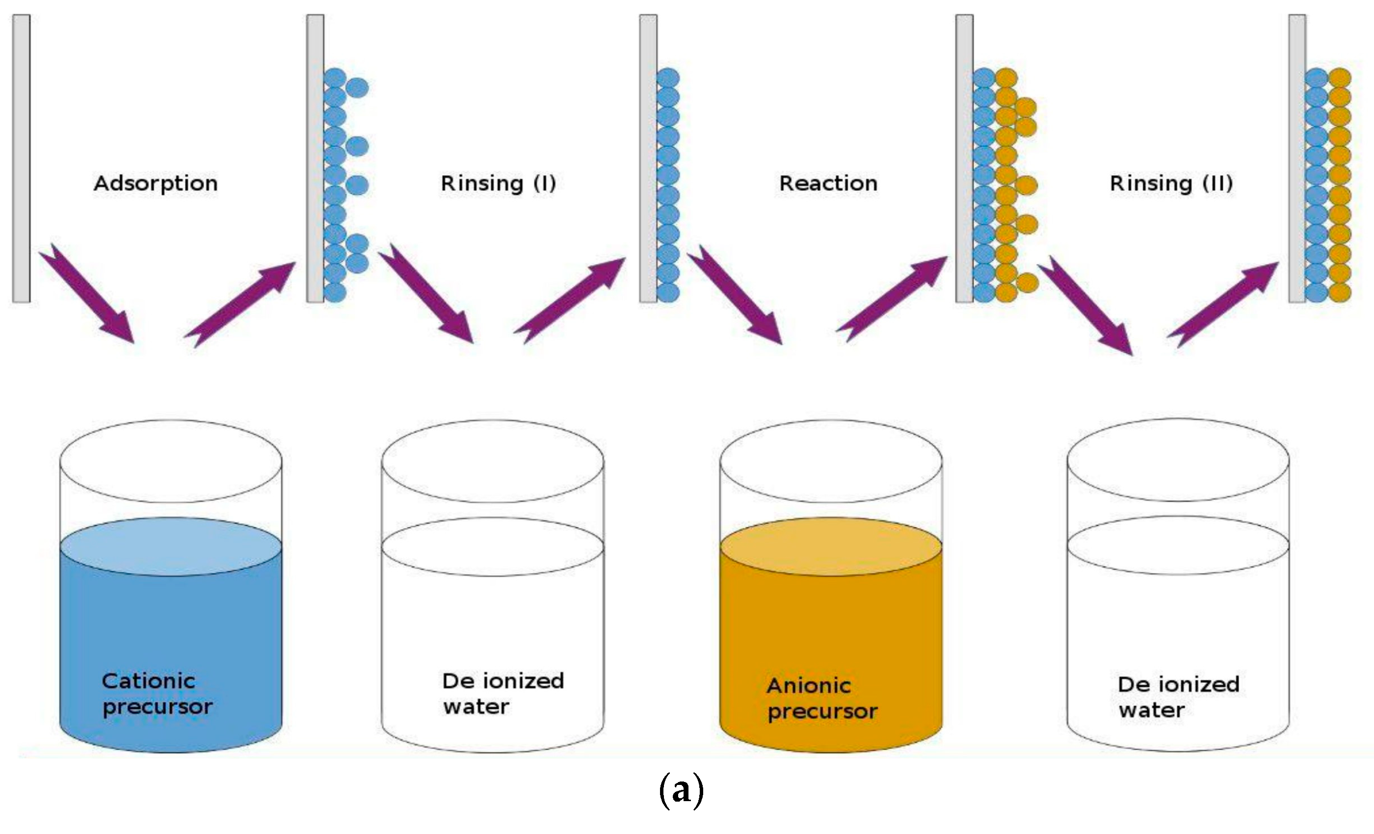
2.1.5. Successive Ionic Layer Adsorption and Reaction (SILAR) Technique
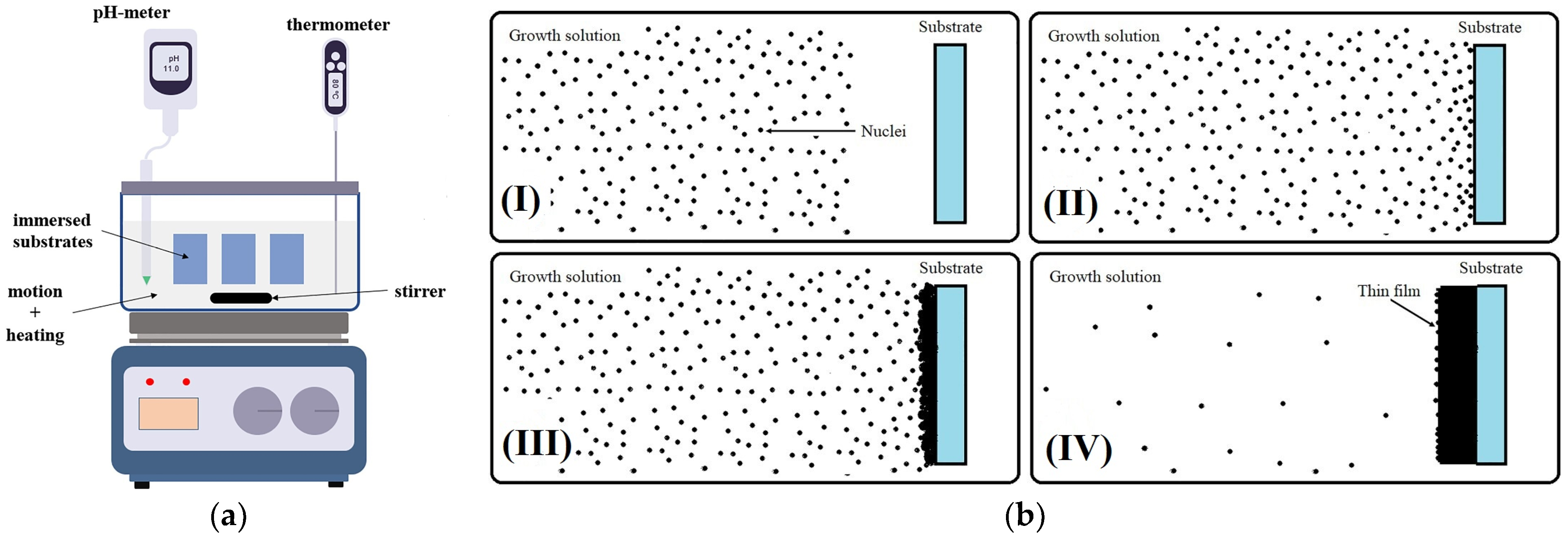
2.1.6. Chemical Bath Deposition (CBD) Technique
2.1.7. Printing Techniques
- Inkjet printing
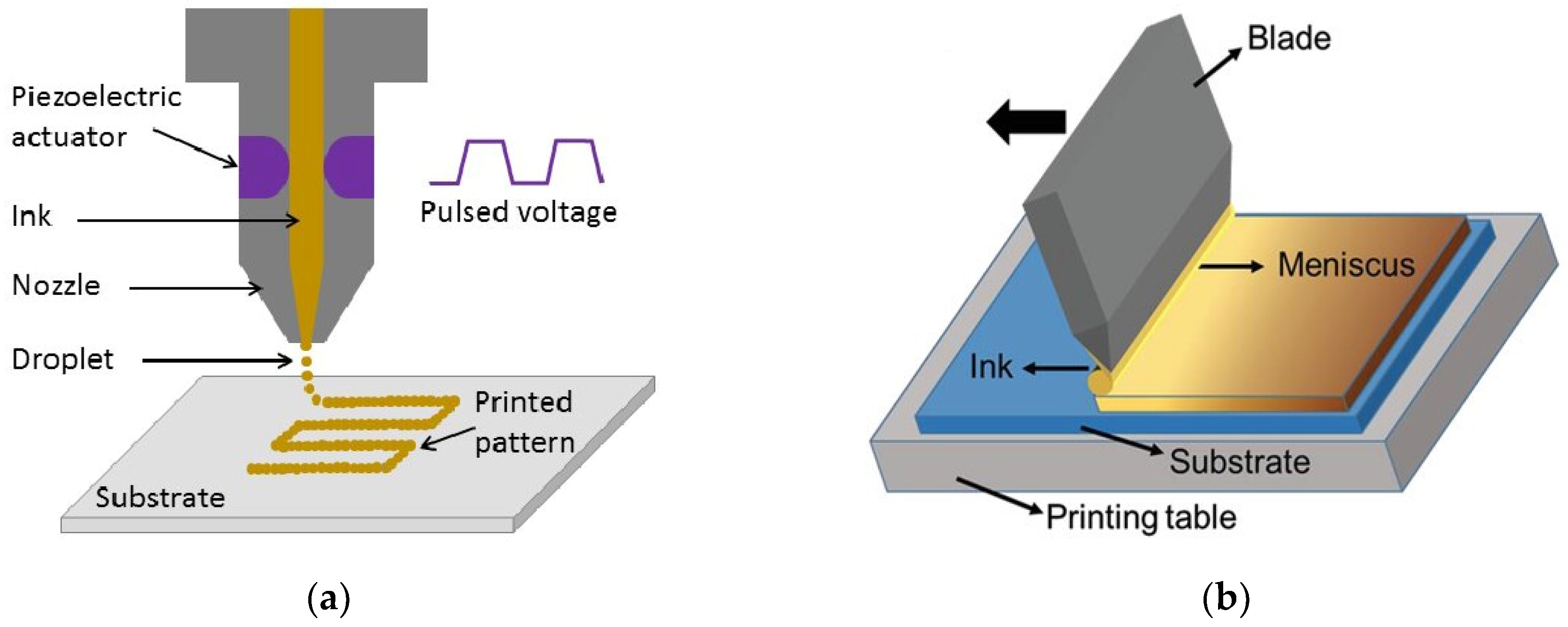

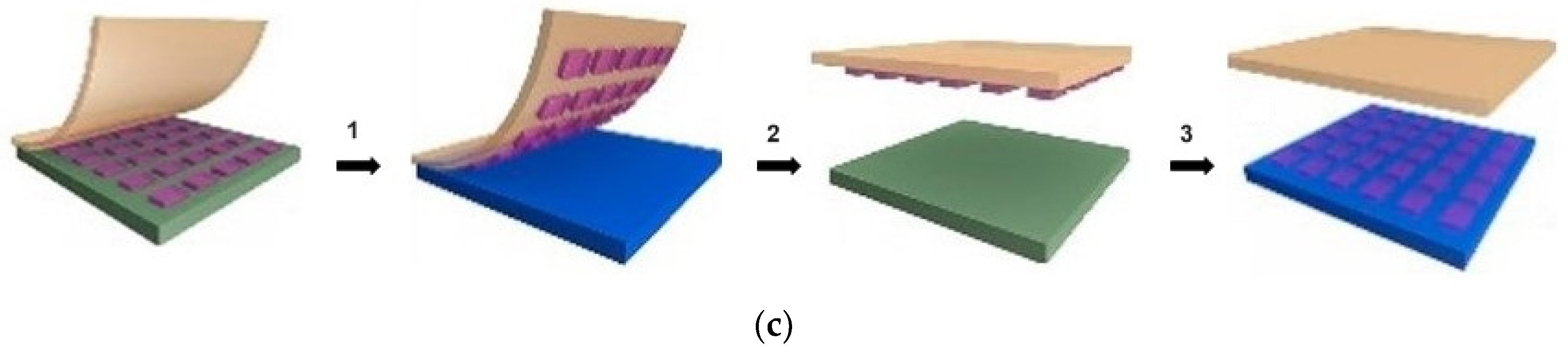
- Transfer printing
- Spray printing technique

| Deposition Method | HTM Thickness [nm] | Device Configuration | Voc [V] | Jsc [mA cm−2] | FF [%] | PCE [%] | Refs. |
|---|---|---|---|---|---|---|---|
| Spin coating | 30 | ITO/CuI/CH3NH3PbI3/C60:BCP/Ag | 0.99 | 22.6 | 71.3 | 16.8 | [90] |
| 30 | ITO/CuI/P3HT:PC61 BM/Ca/Al | 0.55 | 9.02 | 63 | 3.1 | [56] | |
| 30 | ITO/CuI NP/P3HT:PC61 BM/Ca/Al | 0.56 | 9.71 | 63.9 | 3.47 | [56] | |
| ITO/ZnO NP/MEH-PPV:PC61 BM/CuI/Ag | 1.54 | 2.5 | 35 | 1.35 | [91] | ||
| Spin coating [NH3(aq.)] | 30 | ITO/CuI/HaP/PCBM/AZO/Ag | 0.99 | 19.37 | 74 | 14.21 | [92] |
| Spray coating | FTO/TiO2/CH3NH3PbI3−xClx/CuI/A | 0.65 | 21.0 | 33 | 4.5 | [60] | |
| 60 | FTO/c-TiO2/MAPbI3/CuI/Au | 1.03 | 22.78 | 75 | 17.6 | [61] | |
| Drop casting | 1500–2000 | FTO/TiO2/CH3NH3PbI3/CuI/Au | 0.55 | 17.8 | 62 | 6.0 | [66] |
| Doctor blading | 400 | FTO/TiO2/CH3NH3PbI3/CuI/graphite/Cu | 0.78 | 16.7 | 57 | 7.5 | [93] |
| Transfer printing | ITO/SnO2/PVK/CuI/Au | 0.79 | 19.3 | 0.54 | 8.3 | [88] |
- Blade coating (doctor blading)
2.2. Neat Methods (Dry Methods)
2.2.1. Powder Pressing
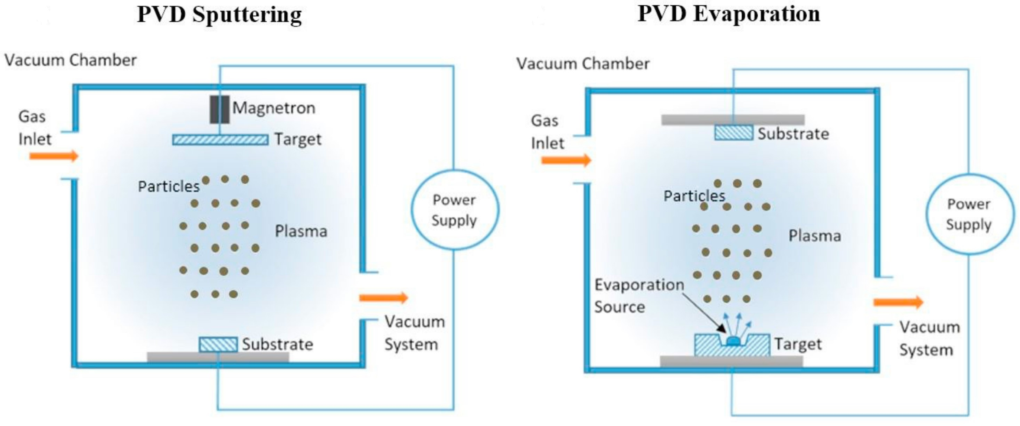
2.2.2. Physical Vapor Deposition Techniques (PVD)
- Thermal evaporation
- Sputter Deposition
- Magnetron sputtering
- Pulsed Laser Deposition (PLD)
3. Conclusions
Funding
Acknowledgments
Conflicts of Interest
References
- Li, B.; Dang, J.; Zhuang, Q.; Lv, Z. Recent Advances in Inorganic Electrochromic Materials from Synthesis to Applications: Critical Review on Functional Chemistry and Structure Engineering. Chem. Asian J. 2022, 17, e202200022. [Google Scholar] [CrossRef]
- Sun, J.; Zhang, B.; Katz, H.E. Materials for Printable, Transparent, and Low-Voltage Transistors. Adv. Funct. Mater. 2011, 21, 29–45. [Google Scholar] [CrossRef]
- Aliprandi, A.; Moreira, T.; Anichini, C.; Stoeckel, M.-A.; Eredia, M.; Sassi, U.; Bruna, M.; Pinheiro, C.; Laia, C.A.T.; Bonacchi, S.; et al. Hybrid Copper-Nanowire–Reduced-Graphene-Oxide Coatings: A “Green Solution” toward Highly Transparent, Highly Conductive, and Flexible Electrodes for (Opto)Electronics. Adv. Mater. 2017, 29, 1703225. [Google Scholar] [CrossRef] [PubMed]
- Al-Jawhari, H.A. Recent Progress of Solution-Processed Copper-based p-Channel Thin-Film Transistors. Adv. Electron. Mater. 2022, 8, 2100893. [Google Scholar] [CrossRef]
- Luo, W.; Zeng, C.; Du, X.; Leng, C.; Yao, W.; Shi, H.; Wei, X.; Du, C.; Lu, S. Copper thiocyanate/copper iodide based hole transport composites with balanced properties for efficient polymer light-emitting diodes. J. Mater. Chem. C 2018, 6, 4895–4902. [Google Scholar] [CrossRef]
- Jamshidi, M.; Bouheriche, J.; Gardner, J.M. Photoluminescent copper(I) iodide alkylpyridine thin films as sensors for volatile halogenated compounds. Front. Chem. 2023, 11, 1330227. [Google Scholar] [CrossRef]
- NREL Chart. March 2023. Available online: https://www.nrel.gov/pv/cell-efficiency.html (accessed on 1 March 2024).
- Kim, J.Y.; Lee, J.-W.; Jung, H.S.; Shin, H.; Park, N.-G. High-Efficiency Perovskite Solar Cells. Chem. Rev. 2020, 120, 7867–7918. [Google Scholar] [CrossRef] [PubMed]
- Correa-Baena, J.-P.; Saliba, M.; Buonassisi, T.; Grätzel, M.; Abate, A.; Tress, W.; Hagfeldt, A. Promises and challenges of perovskite solar cells. Science 2017, 358, 739–744. [Google Scholar] [CrossRef] [PubMed]
- Fortunato, E.; Barquinha, P.; Martins, R. Oxide Semiconductor Thin-Film Transistors: A Review of Recent Advances. Adv. Mater. 2012, 24, 2945–2986. [Google Scholar] [CrossRef]
- Xiong, Z.; Zhang, W.; Cui, Z.; Mei, S.; Hu, Z.; Wen, Z.; He, H.; Duan, Z.; Xie, F.; Guo, R. Eliminating hysteresis effects in flexible organic light-emitting diodes. Org. Electron. 2022, 103, 106467. [Google Scholar] [CrossRef]
- Lee, Y.; Cho, H.; Yoon, H.; Kang, H.; Yoo, H.; Zhou, H.; Jeong, S.; Lee, G.H.; Kim, G.; Go, G.-T.; et al. Advancements in Electronic Materials and Devices for Stretchable Displays. Adv. Mater. Technol. 2023, 8, 2201067. [Google Scholar] [CrossRef]
- Jou, J.-H.; Kumar, S.; Agrawal, A.; Li, T.-H.; Sahoo, S. Approaches for fabricating high efficiency organic light emitting diodes. J. Mater. Chem. C 2015, 3, 2974–3002. [Google Scholar] [CrossRef]
- Zhan, L.; Ying, A.; Qi, Y.; Wu, K.; Tang, Y.; Tan, Y.; Zou, Y.; Xie, G.; Gong, S.; Yang, C. Copper(I) Complex as Sensitizer Enables High-Performance Organic Light-Emitting Diodes with Very Low Efficiency Roll-Off. Adv. Funct. Mater. 2021, 31, 2106345. [Google Scholar] [CrossRef]
- Bi, Y.-G.; Liu, Y.-F.; Zhang, X.-L.; Yin, D.; Wang, W.-Q.; Feng, J.; Sun, H.-B. Ultrathin Metal Films as the Transparent Electrode in ITO-Free Organic Optoelectronic Devices. Adv. Opt. Mater. 2019, 7, 1800778. [Google Scholar] [CrossRef]
- Han, J.; Yang, J.; Gao, W.; Bai, H. Ice-Templated, Large-Area Silver Nanowire Pattern for Flexible Transparent Electrode. Adv. Funct. Mater. 2021, 31, 2010155. [Google Scholar] [CrossRef]
- Lee, S.; Kim, E.H.; Yu, S.; Kim, H.; Park, C.; Lee, S.W.; Han, H.; Jin, W.; Lee, K.; Lee, C.E.; et al. Polymer-Laminated Ti3C2TX MXene Electrodes for Transparent and Flexible Field-Driven Electronics. ACS Nano 2021, 15, 8940–8952. [Google Scholar] [CrossRef]
- Song, J.-K.; Son, D.; Kim, J.; Yoo, Y.J.; Lee, G.J.; Wang, L.; Choi, M.K.; Yang, J.; Lee, M.; Do, K.; et al. Wearable Force Touch Sensor Array Using a Flexible and Transparent Electrode. Adv. Funct. Mater. 2017, 27, 1605286. [Google Scholar] [CrossRef]
- Robertson, J.; Zhang, Z. Doping limits in p-type oxide semiconductors. MRS Bull. 2021, 46, 1037–1043. [Google Scholar] [CrossRef]
- Lee, H.J.; Park, M.-S.; Lee, S.; Kim, B.-J.; Hong, K. Solution-Processed Copper Iodide Film as a p-Type Electrical Conductor and Their Applications. ACS Appl. Electron. Mater. 2022, 4, 1232–1237. [Google Scholar] [CrossRef]
- Ji, Y.; Lee, S.; Lee, H.J.; Choi, K.S.; Jeon, C.; Lee, K.H.; Hong, K. Solution processed vertical p-channel thin film transistors using copper(i) thiocyanate. J. Mater. Chem. C 2020, 8, 5587–5593. [Google Scholar] [CrossRef]
- Benko, F.A.; Koffyberg, F.P. Opto-electronic properties of CuAlO2. J. Phys. Chem. Solids 1984, 45, 57–59. [Google Scholar] [CrossRef]
- Ye, T.; Sun, X.; Zhang, X.; Hao, S. Recent advances of Cu-based hole transport materials and their interface engineering concerning different processing methods in perovskite solar cells. J. Energy Chem. 2021, 62, 459–476. [Google Scholar] [CrossRef]
- Rost, C.; Sieber, I.; Fischer, C.; Lux-Steiner, M.C.; Könenkamp, R. Semiconductor growth on porous substrates. Mater. Sci. Eng. B 2000, 69–70, 570–573. [Google Scholar] [CrossRef]
- Sankapal, B.R.; Goncalves, E.; Ennaoui, A.; Lux-Steiner, M.C. Wide band gap p-type windows by CBD and SILAR methods. Thin Solid Film. 2004, 451–452, 128–132. [Google Scholar] [CrossRef]
- Matebese, F.; Taziwa, R.; Mutukwa, D. Progress on the Synthesis and Application of CuSCN Inorganic Hole Transport Material in Perovskite Solar Cells. Materials 2018, 11, 2592. [Google Scholar] [CrossRef]
- Wang, H.; Yu, Z.; Lai, J.; Song, X.; Yang, X.; Hagfeldt, A.; Sun, L. One plus one greater than two: High-performance inverted planar perovskite solar cells based on a composite CuI/CuSCN hole-transporting layer. J. Mater. Chem. A 2018, 6, 21435–21444. [Google Scholar] [CrossRef]
- Jing, X.; Zhang, Z.; Chen, T.; Luo, J. Review of Inorganic Hole Transport Materials for Perovskite Solar Cells. Energy Technol. 2023, 11, 2201005. [Google Scholar] [CrossRef]
- Keen, D.A.; Hull, S. The high-temperature structural behaviour of copper(I) iodide. J. Phys. Condens. Matter 1995, 7, 5793. [Google Scholar] [CrossRef]
- Zheng-Johansson, J.X.M.; McGreevy, R.L. A molecular dynamics study of ionic conduction in CuI. II. Local ionic motion and conduction mechanisms. Solid State Ion. 1996, 83, 35–48. [Google Scholar] [CrossRef]
- Tennakone, K.; Kumara, G.R.R.A.; Kottegoda, I.R.M.; Perera, V.P.S.; Aponsu, G.M.L.P.; Wijayantha, K.G.U. Deposition of thin conducting films of CuI on glass. Sol. Energy Mater. Sol. Cells 1998, 55, 283–289. [Google Scholar] [CrossRef]
- Bührer, W.; Hälg, W. Crystal Structure of High-Temperature Cuprous Iodide and Cuprous Bromide. In International Symposium on Solid Ionic and Ionic-Electronic Conductors; Armstrong, R.D., Ed.; Pergamon: Oxford, UK, 1977; pp. 701–704. [Google Scholar]
- Seifert, M.; Kawashima, M.; Rödl, C.; Botti, S. Layered CuI: A path to 2D p-type transparent conducting materials. J. Mater. Chem. C 2021, 9, 11284–11291. [Google Scholar] [CrossRef]
- Bernède, J.C.; Cattin, L.; Makha, M.; Jeux, V.; Leriche, P.; Roncali, J.; Froger, V.; Morsli, M.; Addou, M. MoO3/CuI hybrid buffer layer for the optimization of organic solar cells based on a donor–acceptor triphenylamine. Sol. Energy Mater. Sol. Cells 2013, 110, 107–114. [Google Scholar] [CrossRef]
- Konovalov, I.; Szargan, R. Valence band alignment with a small spike at the CuI/CuInS2 interface. Appl. Phys. Lett. 2003, 82, 2088–2090. [Google Scholar] [CrossRef]
- Konovalov, I. Material requirements for CIS solar cells. Thin Solid Film. 2004, 451–452, 413–419. [Google Scholar] [CrossRef]
- Vora-ud, A.; Chaarmart, K.; Kasemsin, W.; Boonkirdram, S.; Seetawan, T. Transparent thermoelectric properties of copper iodide thin films. Phys. B Condens. Matter 2022, 625, 413527. [Google Scholar] [CrossRef]
- Yang, C.; Souchay, D.; Kneiß, M.; Bogner, M.; Wei, H.M.; Lorenz, M.; Oeckler, O.; Benstetter, G.; Fu, Y.Q.; Grundmann, M. Transparent flexible thermoelectric material based on non-toxic earth-abundant p-type copper iodide thin film. Nat. Commun. 2017, 8, 16076. [Google Scholar] [CrossRef] [PubMed]
- Liu, A.; Zhu, H.; Kim, M.-G.; Kim, J.; Noh, Y.-Y. Engineering Copper Iodide (CuI) for Multifunctional p-Type Transparent Semiconductors and Conductors. Adv. Sci. 2021, 8, 2100546. [Google Scholar] [CrossRef] [PubMed]
- Smith, E.; Venkataraman, D. Deleterious Effects of Halides and Solvents used in Electronic Device Fabrication on the Integrity of Copper Iodide Thin-Films**. ChemPlusChem 2022, 87, e202200101. [Google Scholar] [CrossRef]
- Lee, H.-A.; Yatsu, K.; Kim, T.I.; Kwon, H.-I.; Park, I.-J. Synthesis of Vacancy-Controlled Copper Iodide Semiconductor for High-Performance p-Type Thin-Film Transistors. ACS Appl. Mater. Interfaces 2022, 14, 56416–56426. [Google Scholar] [CrossRef]
- Ren, C.; Cao, L.; Wu, T. Meniscus-Guided Deposition of Organic Semiconductor Thin Films: Materials, Mechanism, and Application in Organic Field-Effect Transistors. Small 2023, 19, 2300151. [Google Scholar] [CrossRef]
- Yunus, Y.; Mahadzir, N.A.; Mohamed Ansari, M.N.; Tg Abd Aziz, T.H.; Mohd Afdzaluddin, A.; Anwar, H.; Wang, M.; Ismail, A.G. Review of the Common Deposition Methods of Thin-Film Pentacene, Its Derivatives, and Their Performance. Polymers 2022, 14, 1112. [Google Scholar] [CrossRef]
- Guesnay, Q.; Sahli, F.; Ballif, C.; Jeangros, Q. Vapor deposition of metal halide perovskite thin films: Process control strategies to shape layer properties. APL Mater. 2021, 9, 100703. [Google Scholar] [CrossRef]
- Han, X.; Wu, W.; Chen, H.; Peng, D.; Qiu, L.; Yan, P.; Pan, C. Metal Halide Perovskite Arrays: From Construction to Optoelectronic Applications. Adv. Funct. Mater. 2021, 31, 2005230. [Google Scholar] [CrossRef]
- Xu, X.; Sun, L.; Shen, K.; Zhang, S. Organic and hybrid organic-inorganic flexible optoelectronics: Recent advances and perspectives. Synth. Met. 2019, 256, 116137. [Google Scholar] [CrossRef]
- Zhang, W.; Chen, H.; Guo, X. Precise Control of Interfacial Charge Transport for Building Functional Optoelectronic Devices. Adv. Mater. Technol. 2019, 4, 1800358. [Google Scholar] [CrossRef]
- Takahashi, K.; Suzuki, Y. Perovskite solar cells with CuI inorganic hole conductor. Jpn. J. Appl. Phys. 2017, 56, 08MC04. [Google Scholar] [CrossRef]
- Nur Amalina, M.; Azman, M.A.; Rusop, M.M. Effect of the Precursor Solution Concentration of CuI Thin Film Deposited by Spin Coating Method. Adv. Mater. Res. 2012, 364, 417–421. [Google Scholar] [CrossRef]
- Zhao, K.; Ngongang Ndjawa, G.O.; Jagadamma, L.K.; Labban, A.E.; Hu, H.; Wang, Q.; Li, R.; Abdelsamie, M.; Beaujuge, P.M.; Amassian, A. Highly efficient organic solar cells based on a robust room-temperature solution-processed copper iodide hole transporter. Nano Energy 2015, 16, 458–469. [Google Scholar] [CrossRef]
- Song, J.; Hu, W.; Li, Z.; Wang, X.-F.; Tian, W. A double hole-transport layer strategy toward efficient mixed tin-lead iodide perovskite solar cell. Sol. Energy Mater. Sol. Cells 2020, 207, 110351. [Google Scholar] [CrossRef]
- Chauhan, A.; Oudhia, A.; Shrivastav, A.K. Analysis of eco-friendly tin-halide Cs2SnI6-based perovskite solar cell with all-inorganic charge selective layers. J. Mater. Sci. Mater. Electron. 2022, 33, 1670–1685. [Google Scholar] [CrossRef]
- Inudo, S.; Miyake, M.; Hirato, T. Electrical properties of CuI films prepared by spin coating. Phys. Status Solidi (A) 2013, 210, 2395–2398. [Google Scholar] [CrossRef]
- Liu, A.; Zhu, H.; Park, W.-T.; Kang, S.-J.; Xu, Y.; Kim, M.-G.; Noh, Y.-Y. Room-Temperature Solution-Synthesized p-Type Copper(I) Iodide Semiconductors for Transparent Thin-Film Transistors and Complementary Electronics. Adv. Mater. 2018, 30, 1802379. [Google Scholar] [CrossRef]
- Lee, H.J.; Lee, S.; Lee, K.H.; Hong, K. Amorphous copper iodide: A p-type semiconductor for solution processed p-channel thin-film transistors and inverters. J. Mater. Chem. C 2022, 10, 7815–7821. [Google Scholar] [CrossRef]
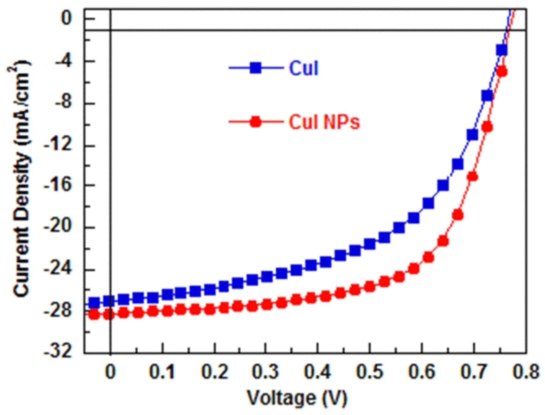
- Zhong, Y.; Li, Y.; Lan, X.; Wang, J.; Wang, J.; Zhang, Y. Enhancing Efficiency and Stability of Polymer Solar Cells Based on CuI Nanoparticles as the Hole Transport Layer. IEEE J. Photovolt. 2021, 11, 668–673. [Google Scholar] [CrossRef]
- Byranvand, M.M.; Kim, T.; Song, S.; Kang, G.; Ryu, S.U.; Park, T. p-Type CuI Islands on TiO2 Electron Transport Layer for a Highly Efficient Planar-Perovskite Solar Cell with Negligible Hysteresis. Adv. Energy Mater. 2018, 8, 1702235. [Google Scholar] [CrossRef]
- Li, M.; Wang, Z.-K.; Yang, Y.-G.; Hu, Y.; Feng, S.-L.; Wang, J.-M.; Gao, X.-Y.; Liao, L.-S. Copper Salts Doped Spiro-OMeTAD for High-Performance Perovskite Solar Cells. Adv. Energy Mater. 2016, 6, 1601156. [Google Scholar] [CrossRef]
- Choudhury, A.; Nagar, M.R.; The, L.; Lin, Y.-J.; Liang, Y.-H.; Chen, S.-Z.; Jou, J.-H. Nanocrystalline copper iodide enabling high-efficiency organic LEDs. Org. Electron. 2022, 111, 106668. [Google Scholar] [CrossRef]
- Huangfu, M.; Shen, Y.; Zhu, G.; Xu, K.; Cao, M.; Gu, F.; Wang, L. Copper iodide as inorganic hole conductor for perovskite solar cells with different thickness of mesoporous layer and hole transport layer. Appl. Surf. Sci. 2015, 357, 2234–2240. [Google Scholar] [CrossRef]
- Li, X.; Yang, J.; Jiang, Q.; Chu, W.; Zhang, D.; Zhou, Z.; Xin, J. Synergistic Effect to High-Performance Perovskite Solar Cells with Reduced Hysteresis and Improved Stability by the Introduction of Na-Treated TiO2 and Spraying-Deposited CuI as Transport Layers. ACS Appl. Mater. Interfaces 2017, 9, 41354–41362. [Google Scholar] [CrossRef]
- Lee, K.; Gyu Oh, J.; Kim, D.; Baek, J.; Ho Kim, I.; Nam, S.; Jeong, Y.J.; Jang, J. Copper iodide and oxide semiconductor thin films patterned by spray-spin coating for fabricating complementary inverters: Improving stability with passivation layers. Appl. Surf. Sci. 2023, 608, 155081. [Google Scholar] [CrossRef]
- Kaliyaraj Selva Kumar, A.; Zhang, Y.; Li, D.; Compton, R.G. A mini-review: How reliable is the drop casting technique? Electrochem. Commun. 2020, 121, 106867. [Google Scholar] [CrossRef]
- Zuo, C.; Scully, A.D.; Gao, M. Drop-Casting Method to Screen Ruddlesden–Popper Perovskite Formulations for Use in Solar Cells. ACS Appl. Mater. Interfaces 2021, 13, 56217–56225. [Google Scholar] [CrossRef] [PubMed]
- Chen, G.; Wang, L.; Sheng, X.; Liu, H.; Pi, X.; Yang, D. Chemical synthesis of Cu(In) metal inks to prepare CuInS2 thin films and solar cells. J. Alloys Compd. 2010, 507, 317–321. [Google Scholar] [CrossRef]
- Christians, J.A.; Fung, R.C.M.; Kamat, P.V. An Inorganic Hole Conductor for Organo-Lead Halide Perovskite Solar Cells. Improved Hole Conductivity with Copper Iodide. J. Am. Chem. Soc. 2014, 136, 758–764. [Google Scholar] [CrossRef] [PubMed]
- Nicolau, Y.F. Solution deposition of thin solid compound films by a successive ionic-layer adsorption and reaction process. Appl. Surf. Sci. 1985, 22–23, 1061–1074. [Google Scholar] [CrossRef]
- Jose, E.; Kumar, M.C.S. Room-temperature wide-range luminescence and structural, optical, and electrical properties of SILAR deposited Cu-Zn-S nano-structured thin films. In Proceedings of the SPIE Nanoscience + Engineering, San Diego, CA, USA, 28 August–1 September 2016; Volume 9929. [Google Scholar]
- Klochko, N.P.; Barbash, V.A.; Petrushenko, S.I.; Kopach, V.R.; Klepikova, K.S.; Zhadan, D.O.; Yashchenko, O.V.; Dukarov, S.V.; Sukhov, V.M.; Khrypunova, A.L. Thermoelectric textile devices with thin films of nanocellulose and copper iodide. J. Mater. Sci. Mater. Electron. 2021, 32, 23246–23265. [Google Scholar] [CrossRef]
- Dhere, S.L.; Latthe, S.S.; Kappenstein, C.; Mukherjee, S.K.; Rao, A.V. Comparative studies on p-type CuI grown on glass and copper substrate by SILAR method. Appl. Surf. Sci. 2010, 256, 3967–3971. [Google Scholar] [CrossRef]
- Klochko, N.P.; Barbash, V.A.; Klepikova, K.S.; Kopach, V.R.; Yashchenko, O.V.; Zhadan, D.O.; Petrushenko, S.I.; Dukarov, S.V.; Sukhov, V.M.; Khrypunova, A.L. Nanostructured CuI thin films on biodegradable nanocellulose flexible substrates for UV-shielding applications. Mol. Cryst. Liq. Cryst. 2021, 717, 80–91. [Google Scholar] [CrossRef]
- Klochko, N.; Klepikova, K.; Zhadan, D.; Kopach, V.; Khrypunova, I.; Petrushenko, S.; Dukarov, S.; Lyubov, V.; Khrypunova, A. Nanostructured ZnO and CuI thin films on poly (ethylene terephthalate) tapes for UV-shielding applications. Nano- Electron. Phys. 2020, 12, 03007. [Google Scholar] [CrossRef] [PubMed]
- Puscher, C. Ueber ein neues und billiges verfahren, ohne anwendung von farben verschiedene metalle (wie gold, silber, kupfer, argentan, messing, tombak, eisen, zink) mit prachtvollen lüsterfarben zu überziehen. Polytech J. 1868, 190. [Google Scholar]
- Oliva, A.I.; González-Chan, I.J.; Várguez, P.E.; Trejo-Ramos, A.I.; Oliva-Avilés, A.I. The chemical process for materials deposition in aqueous solution: A review. Surf. Eng. 2022, 38, 907–929. [Google Scholar] [CrossRef]
- Pawar, S.M.; Pawar, B.S.; Kim, J.H.; Joo, O.-S.; Lokhande, C.D. Recent status of chemical bath deposited metal chalcogenide and metal oxide thin films. Curr. Appl. Phys. 2011, 11, 117–161. [Google Scholar] [CrossRef]
- Bulakhe, R.N.; Shinde, N.M.; Thorat, R.D.; Nikam, S.S.; Lokhande, C.D. Deposition of copper iodide thin films by chemical bath deposition (CBD) and successive ionic layer adsorption and reaction (SILAR) methods. Curr. Appl. Phys. 2013, 13, 1661–1667. [Google Scholar] [CrossRef]
- Reddy, G.; Katakam, R.; Devulapally, K.; Jones, L.A.; Della Gaspera, E.; Upadhyaya, H.M.; Islavath, N.; Giribabu, L. Ambient stable, hydrophobic, electrically conductive porphyrin hole-extracting materials for printable perovskite solar cells. J. Mater. Chem. C 2019, 7, 4702–4708. [Google Scholar] [CrossRef]
- Luo, X.; Zeng, Z.; Wang, X.; Xiao, J.; Gan, Z.; Wu, H.; Hu, Z. Preparing two-dimensional nano-catalytic combustion patterns using direct inkjet printing. J. Power Sources 2014, 271, 174–179. [Google Scholar] [CrossRef]
- Wang, J.; Li, D.; Luo, Y.; Wang, J.; Peng, J. Inkjet Printing Efficient Defined-Pixel Matrix Perovskite Light-Emitting Diodes with a Polar Polymer Modification Layer. Adv. Mater. Technol. 2022, 7, 2200370. [Google Scholar] [CrossRef]
- Samantaray, N.; Parida, B.; Soga, T.; Sharma, A.; Kapoor, A.; Najar, A.; Singh, A. Recent Development and Directions in Printed Perovskite Solar Cells. Phys. Status Solidi (A) 2022, 219, 2100629. [Google Scholar] [CrossRef]
- Choi, C.-H.; Gorecki, J.Y.; Fang, Z.; Allen, M.; Li, S.; Lin, L.-Y.; Cheng, C.-C.; Chang, C.-H. Low-temperature, inkjet printed p-type copper(i) iodide thin film transistors. J. Mater. Chem. C 2016, 4, 10309–10314. [Google Scholar] [CrossRef]
- Jabari, E.; Ahmed, F.; Liravi, F.; Secor, E.B.; Lin, L.; Toyserkani, E. 2D printing of graphene: A review. 2D Materials 2019, 6, 042004. [Google Scholar] [CrossRef]
- Parida, B.; Singh, A.; Kalathil Soopy, A.K.; Sangaraju, S.; Sundaray, M.; Mishra, S.; Liu, S.; Najar, A. Recent Developments in Upscalable Printing Techniques for Perovskite Solar Cells. Adv. Sci. 2022, 9, 2200308. [Google Scholar] [CrossRef]
- Tong, S.; Sun, J.; Yang, J. Printed Thin-Film Transistors: Research from China. ACS Appl. Mater. Interfaces 2018, 10, 25902–25924. [Google Scholar] [CrossRef] [PubMed]
- Carlson, A.; Bowen, A.M.; Huang, Y.; Nuzzo, R.G.; Rogers, J.A. Transfer Printing Techniques for Materials Assembly and Micro/Nanodevice Fabrication. Adv. Mater. 2012, 24, 5284–5318. [Google Scholar] [CrossRef] [PubMed]
- Jakob, T.; Polywka, A.; Stegers, L.; Akdeniz, E.; Kropp, S.; Frorath, M.; Trost, S.; Schneider, T.; Riedl, T.; Görrn, P. Transfer printing of electrodes for organic devices: Nanoscale versus macroscale continuity. Appl. Phys. A 2015, 120, 503–508. [Google Scholar] [CrossRef]
- Chen, L.; Degenaar, P.; Bradley, D.D.C. Polymer Transfer Printing: Application to Layer Coating, Pattern Definition, and Diode Dark Current Blocking. Adv. Mater. 2008, 20, 1679–1683. [Google Scholar] [CrossRef]
- Srivastava, R.P.; Jung, H.-S.; Khang, D.-Y. Transfer-Printed Cuprous Iodide (CuI) Hole Transporting Layer for Low Temperature Processed Perovskite Solar Cells. Nanomaterials 2022, 12, 1467. [Google Scholar] [CrossRef] [PubMed]
- Bae, E.J.; Kim, J.; Han, M.; Kang, Y.H. Precision Doping of Iodine for Highly Conductive Copper(I) Iodide Suitable for the Spray-Printable Thermoelectric Power Generators. ACS Mater. Lett. 2023, 5, 2009–2018. [Google Scholar] [CrossRef]
- Sun, W.; Ye, S.; Rao, H.; Li, Y.; Liu, Z.; Xiao, L.; Chen, Z.; Bian, Z.; Huang, C. Room-temperature and solution-processed copper iodide as the hole transport layer for inverted planar perovskite solar cells. Nanoscale 2016, 8, 15954–15960. [Google Scholar] [CrossRef] [PubMed]
- Salem, A.M.S.; El-Sheikh, S.M.; Harraz, F.A.; Ebrahim, S.; Soliman, M.; Hafez, H.S.; Ibrahim, I.A.; Abdel-Mottaleb, M.S.A. Inverted polymer solar cell based on MEH-PPV/PC61BM coupled with ZnO nanoparticles as electron transport layer. Appl. Surf. Sci. 2017, 425, 156–163. [Google Scholar] [CrossRef]
- Khadka, D.B.; Shirai, Y.; Yanagida, M.; Miyano, K. Ammoniated aqueous precursor ink processed copper iodide as hole transport layer for inverted planar perovskite solar cells. Sol. Energy Mater. Sol. Cells 2020, 210, 110486. [Google Scholar] [CrossRef]
- Sepalage, G.A.; Meyer, S.; Pascoe, A.; Scully, A.D.; Huang, F.; Bach, U.; Cheng, Y.-B.; Spiccia, L. Copper(I) Iodide as Hole-Conductor in Planar Perovskite Solar Cells: Probing the Origin of J–V Hysteresis. Adv. Funct. Mater. 2015, 25, 5650–5661. [Google Scholar] [CrossRef]
- Uthayaraj, S.; Karunarathne, D.G.B.C.; Kumara, G.R.A.; Murugathas, T.; Rasalingam, S.; Rajapakse, R.M.G.; Ravirajan, P.; Velauthapillai, D. Powder Pressed Cuprous Iodide (CuI) as A Hole Transporting Material for Perovskite Solar Cells. Materials 2019, 12, 2037. [Google Scholar] [CrossRef] [PubMed]
- Han, X.; Lu, Y.; Liu, Y.; Wu, M.; Li, Y.; Wang, Z.; Cai, K. CuI/Nylon Membrane Hybrid Film with Large Seebeck Effect. Chin. Phys. Lett. 2021, 38, 126701. [Google Scholar] [CrossRef]
- Baptista, A.; Silva, F.J.G.; Porteiro, J.; Míguez, J.L.; Pinto, G.; Fernandes, L. On the Physical Vapour Deposition (PVD): Evolution of Magnetron Sputtering Processes for Industrial Applications. Procedia Manuf. 2018, 17, 746–757. [Google Scholar] [CrossRef]
- Marshall, K.P.; Walton, R.I.; Hatton, R.A. Tin perovskite/fullerene planar layer photovoltaics: Improving the efficiency and stability of lead-free devices. J. Mater. Chem. A 2015, 3, 11631–11640. [Google Scholar] [CrossRef]
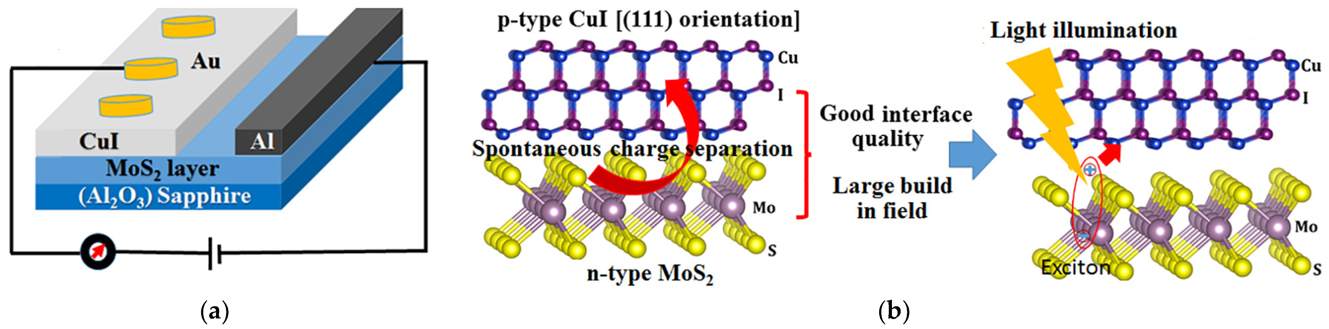
- Mahyavanshi, R.D.; Desai, P.; Ranade, A.; Tanemura, M.; Kalita, G. Observing Charge Transfer Interaction in CuI and MoS2 Heterojunction for Photoresponsive Device Application. ACS Appl. Electron. Mater. 2019, 1, 302–310. [Google Scholar] [CrossRef]
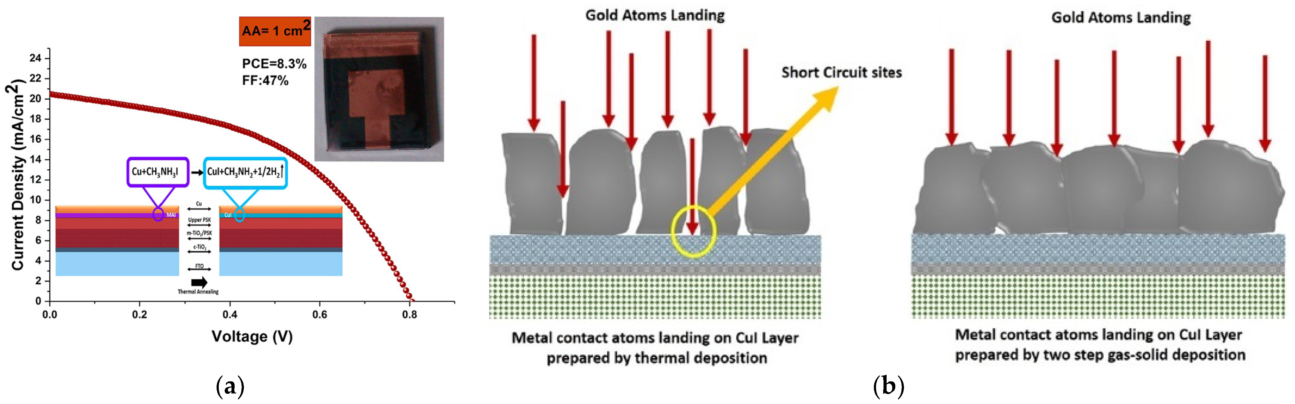
- Nazari, P.; Ansari, F.; Abdollahi Nejand, B.; Ahmadi, V.; Payandeh, M.; Salavati-Niasari, M. Physicochemical Interface Engineering of CuI/Cu as Advanced Potential Hole-Transporting Materials/Metal Contact Couples in Hysteresis-Free Ultralow-Cost and Large-Area Perovskite Solar Cells. J. Phys. Chem. C 2017, 121, 21935–21944. [Google Scholar] [CrossRef]
- Gharibzadeh, S.; Nejand, B.A.; Moshaii, A.; Mohammadian, N.; Alizadeh, A.H.; Mohammadpour, R.; Ahmadi, V.; Alizadeh, A. Two-Step Physical Deposition of a Compact CuI Hole-Transport Layer and the Formation of an Interfacial Species in Perovskite Solar Cells. ChemSusChem 2016, 9, 1929–1937. [Google Scholar] [CrossRef] [PubMed]
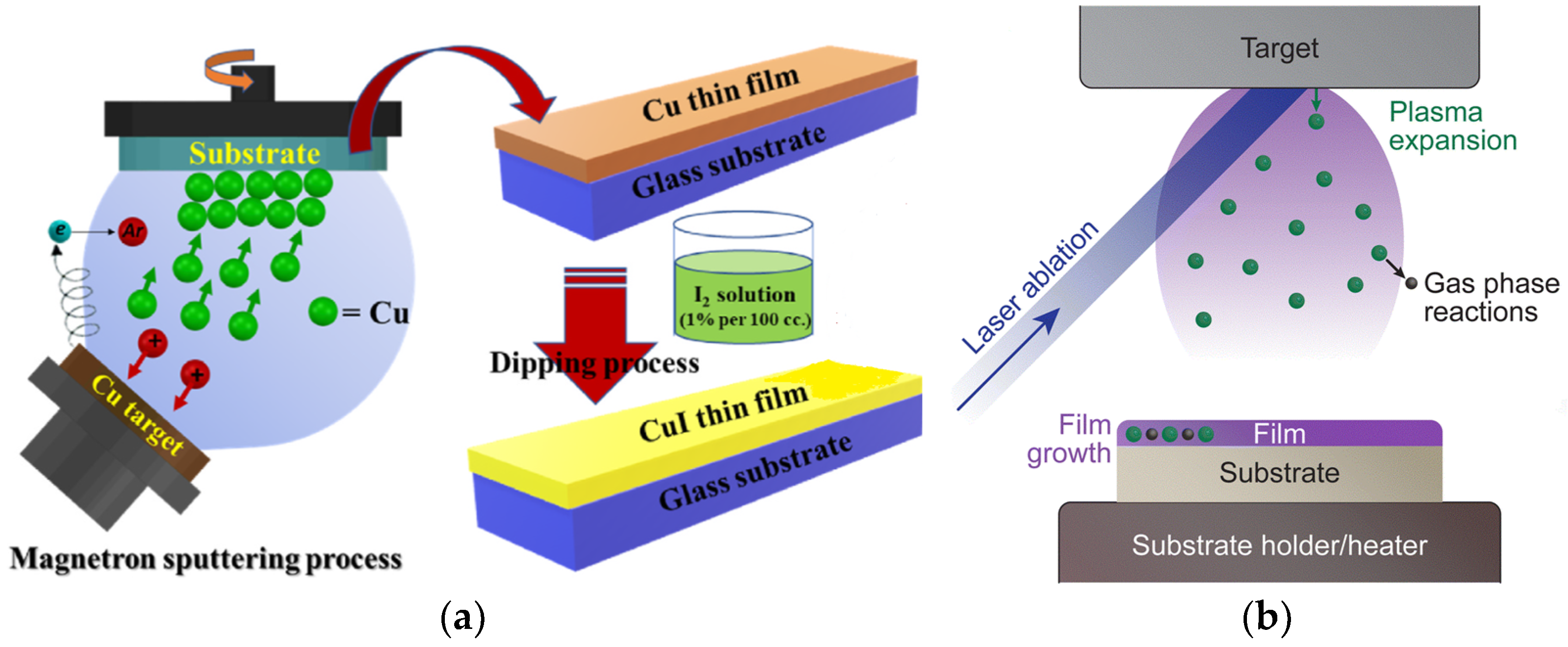
- Ahn, K.; Kim, G.H.; Kim, S.-J.; Kim, J.; Ryu, G.-S.; Lee, P.; Ryu, B.; Cho, J.Y.; Kim, Y.-H.; Kang, J.; et al. Highly Conductive p-Type Transparent Conducting Electrode with Sulfur-Doped Copper Iodide. Chem. Mater. 2022, 34, 10517–10527. [Google Scholar] [CrossRef]
- Wang, M.; Wei, H.; Wu, Y.; Yang, C.; Han, P.; Juan, F.; Chen, Y.; Xu, F.; Cao, B. Highly transparent and conductive γ-CuI films grown by simply dipping copper films into iodine solution. Phys. B Condens. Matter 2019, 573, 45–48. [Google Scholar] [CrossRef]
- Yang, C.; Kneiβ, M.; Lorenz, M.; Grundmann, M. Room-temperature synthesized copper iodide thin film as degenerate p-type transparent conductor with a boosted figure of merit. Proc. Natl. Acad. Sci. USA 2016, 113, 12929–12933. [Google Scholar] [CrossRef]
- Schein, F.-L.; von Wenckstern, H.; Grundmann, M. Transparent p-CuI/n-ZnO heterojunction diodes. Appl. Phys. Lett. 2013, 102, 092109. [Google Scholar] [CrossRef]
- Baek, S.-D.; Kwon, D.-K.; Kim, Y.C.; Myoung, J.-M. Violet Light-Emitting Diodes Based on p-CuI Thin Film/n-MgZnO Quantum Dot Heterojunction. ACS Appl. Mater. Interfaces 2020, 12, 6037–6047. [Google Scholar] [CrossRef] [PubMed]
- Baek, S.-D.; Myoung, J.-M. Enhanced luminescence of quasi-double heterostructured violet light-emitting diodes based on n-Mg0.027Zn0.973O QD and p-Cu1-xZnxI thin films fabricated via simple thermal diffusion and iodination processes. Chem. Eng. J. 2021, 413, 127401. [Google Scholar] [CrossRef]
- Mahdy, B.; Isomura, M.; Kaneko, T. Fabrication of inverted planar perovskite solar cells using the iodine/ethanol solution method for copper iodide as a hole transport layer. Jpn. J. Appl. Phys. 2023, 62, SK1016. [Google Scholar] [CrossRef]
- Shepelin, N.A.; Tehrani, Z.P.; Ohannessian, N.; Schneider, C.W.; Pergolesi, D.; Lippert, T. A practical guide to pulsed laser deposition. Chem. Soc. Rev. 2023, 52, 2294–2321. [Google Scholar] [CrossRef] [PubMed]
- Zhu, B.L.; Zhao, X.Z. Transparent conductive CuI thin films prepared by pulsed laser deposition. Phys. Status Solidi (A) 2011, 208, 91–96. [Google Scholar] [CrossRef]
- Rusop, M.; Shirata, T.; Sirimanne, P.M.; Soga, T.; Jimbo, T. Properties of Pulsed-Laser-Deposited CuI and Characteristics of Constructed Dye-Sensitized TiO2|Dye|CuI Solid-State Photovoltaic Solar Cells. Jpn. J. Appl. Phys. 2003, 42, 4966. [Google Scholar] [CrossRef]
- Storm, P.; Bar, M.S.; Benndorf, G.; Selle, S.; Yang, C.; von Wenckstern, H.; Grundmann, M.; Lorenz, M. High mobility, highly transparent, smooth, p-type CuI thin films grown by pulsed laser deposition. APL Mater. 2020, 8, 091115. [Google Scholar] [CrossRef]
- Sirimanne, P.M.; Rusop, M.; Shirata, T.; Soga, T.; Jimbo, T. Characterization of transparent conducting CuI thin films prepared by pulse laser deposition technique. Chem. Phys. Lett. 2002, 366, 485–489. [Google Scholar] [CrossRef]
- Wang, H.; Yu, Z.; Jiang, X.; Li, J.; Cai, B.; Yang, X.; Sun, L. Efficient and Stable Inverted Planar Perovskite Solar Cells Employing CuI as Hole-Transporting Layer Prepared by Solid–Gas Transformation. Energy Technol. 2017, 5, 1836–1843. [Google Scholar] [CrossRef]


| HTM Deposition Method | HTM Thickness [nm] | Device Configuration | Voc [V] | Jsc [mA cm−2] | FF [%] | PCE [%] | Refs. |
|---|---|---|---|---|---|---|---|
| Powder pressing | 1 mm | FTO-Pt-coated/CuI/PVK/m-TiO2/FTO | 0.67 | 24.23 | 50 | 8.1 | [94] |
| Thermal evaporation | 70 | ITO/CuI/CsSnI3/PCBM/BCP/Al | 0.36 | 8.94 | 54 | 1.72 | [97] |
| 40 | FTO/CuI/PVK/PCBM/PEI-Ag | 1.04 | 20.9 | 68 | 14.7 | [113] | |
| Thermal evaporation/solid–gas reaction | 1200 (Cu) | FTO/TiO2/CH3NH3PbI3/CuI/Au | 0.73 | 32.72 | 31 | 7.40 | [100] |
| 120 (Cu) | FTO/TiO2/CH3NH3PbI3/CuI/Cu | 0.85 | 22.99 | 47 | 9.24 | [99] | |
| Magnetron sputtering | 440 | FTO/CuI/PVK/PCBM/Au | 0.49 | 4.6 | 34 | 0.76 | [107] |
| Pulsed laser | 100 | ITO/TiO2/dye/CuI/Pt | 0.48 | 12.2 | 48 | 2.8 | [110] |
Disclaimer/Publisher’s Note: The statements, opinions and data contained in all publications are solely those of the individual author(s) and contributor(s) and not of MDPI and/or the editor(s). MDPI and/or the editor(s) disclaim responsibility for any injury to people or property resulting from any ideas, methods, instructions or products referred to in the content. |
© 2024 by the authors. Licensee MDPI, Basel, Switzerland. This article is an open access article distributed under the terms and conditions of the Creative Commons Attribution (CC BY) license (https://creativecommons.org/licenses/by/4.0/).
Share and Cite
Jamshidi, M.; Gardner, J.M. Copper(I) Iodide Thin Films: Deposition Methods and Hole-Transporting Performance. Molecules 2024, 29, 1723. https://doi.org/10.3390/molecules29081723
Jamshidi M, Gardner JM. Copper(I) Iodide Thin Films: Deposition Methods and Hole-Transporting Performance. Molecules. 2024; 29(8):1723. https://doi.org/10.3390/molecules29081723
Chicago/Turabian StyleJamshidi, Mahboubeh, and James M. Gardner. 2024. "Copper(I) Iodide Thin Films: Deposition Methods and Hole-Transporting Performance" Molecules 29, no. 8: 1723. https://doi.org/10.3390/molecules29081723
APA StyleJamshidi, M., & Gardner, J. M. (2024). Copper(I) Iodide Thin Films: Deposition Methods and Hole-Transporting Performance. Molecules, 29(8), 1723. https://doi.org/10.3390/molecules29081723