Article

Optimal Energy Efficiency Tracking in the Energy-Stored Quasi-Z-Source Inverter

1
College of Electrical Engineering, Zhejiang University, Hangzhou 310027, China
2
Department of Energy Engineering, Zhejiang University, Hangzhou 310027, China
*
Author to whom correspondence should be addressed.
Energies 2020, 13(22), 5902; https://doi.org/10.3390/en13225902
Submission received: 23 September 2020 / Revised: 30 October 2020 / Accepted: 10 November 2020 / Published: 12 November 2020

Abstract

:
In this paper, the interaction between the energy storage (ES) power distribution and system efficiency enhancement is researched based on the energy stored quasi-Z-source inverter. The corresponding current counteraction, stress reduction, power loss profile, and efficiency enhancement around the embedded energy storage units are studied in details. Firstly, the current counteraction effect on the device current is presented with the embedded ES source. The corresponding reduction in the device current stress is revealed. Then, the detailed device power loss expressions with current redistribution in the impedance network are explored mathematically. A quasi-inverted-trapezoidal power loss profile is found with the embedded source power distribution. To further increase the overall system efficiency, an optimal energy efficiency tracking strategy is proposed for the ES-qZSI (energy-stored quasi-Z-source inverter) based on the power distribution control. Both the simulation and the experiment verified that the power loss is reduced by over 40% through the proposed efficiency enhancement method. The device current and loss analysis for the embedding of energy storage can also be extended to the operating range optimization in other ES systems.

1. Introduction

The energy storage system (ESS) has been attractive in various ancillary services for renewable energy generation and other applications [1,2]. To supply energy for longer durations and improve the benefits provided by multi-energy storage systems, the optimal overall efficiency should be achieved considering each subordinate energy storage. Different from the power generation applications with maximum power point tracking (MPPT) requirement, like PV and wind turbines, an ideal energy storage system usually aims to achieve maximum energy efficiency tracking (MEET) [3,4]. A MEET scheme for the micro-grid was studied [5] through the optimal power distribution. The optimization criterion is based the system achieving high efficiency with a battery at a low state of charge (SOC). Improving efficiency through power distribution regulation was proposed [6]. These power distribution methods were also applied for applications such as electric vehicles and elevators [7,8,9]. MEET has proved to be effective for power conversion system (PCS) applications in AC or DC micro-grids. However, owing to the fluctuation in output power and SOC, the MEET for ESSs does not currently have the capability to handle a wide operation range.
The energy-stored quasi-Z-source inverter (ES-qZSI) is characterized by single-stage power conversion and high efficiency. Its operation principle with multiple energy storages, including both battery and ultra-capacitor, has been demonstrated [10,11]. The topology was researched widely for applications such as photovoltaic power generation and electric vehicles [12,13,14]. Methods like soft-switching and modulation strategy, aiming at device current stress reduction, were applied for efficiency improvement [15,16,17]. An optimal power distribution to improve efficiency has been given in [18,19], but the principle and operation range are still obscure due to the lack of interaction studies on the impedance network, the switching device stress, and the energy storage units.
In this paper, the principle for the current counteraction and stress reduction around the energy-storage units embedding in the ES-qZSI is studied in detail. The device power loss with the current redistribution in the impedance network is explored mathematically. A quasi-inverted-trapezoidal power loss profile is found with power distribution between the input source and the embedded source. Finally, a wide range optimal energy efficiency tracking technology in the ES-qZSI is proposed. The effectiveness of the theatrical analysis and proposed method are validated by both a simulation and experiment. The power loss of the ES-qZSI can be reduced by more than 40% compared with the conventional qZSI.

2. Principle of Current Counteraction in ES-qZSI

The circuit of the ES-qZSI is demonstrated in Figure 1. The input of the ES-qZSI, denoted as source 1, is connected with a DC source, such as PV, which is similar to the conventional qZSI topology. Compared with the conventional qZSI topology, an energy storage unit, such as a battery, is embedded parallel with the capacitor C2 in the ES-qZSI and is denoted as source 2.
The system can be separated into two parts by the DC-bus based on the system operation, as shown as the AC and DC sides in Figure 1. In the shoot-through (ST) state, the switch S7 in the DC side turns off and at least one phase leg in the AC side is short-circuited. In the non-shoot-through (NST) states, S7 turns on and S1S6 operate like the conventional voltage source inverter (VSI) [18].
Due to the embedded energy storage unit, Vbus is clamped by the voltages of sources 1 and 2. Then S7 and the ST state are adopted to distribute the power between the two sources. Based on the power conservation, the source current distribution in the ES-qZSI is derived as Equation (1) [18], where D represents the ST duty ratio, Isource1 represents the current from source 1, and Isource2 represents the current from source 2. The current allocation of the two sources is achieved through the regulation of the ST duty ratio.
I bus = ( 1 2 D ) I source 1 + D I source 2
Compared with the conventional qZSI, the current from source 2 has an impact on the internal current distribution of the impedance network on the DC side. For the traditional qZSI, the inductor current IL2 is clamped by the inductor current IL1 due to the zero average currents through C1 and C2, as shown in Equation (2), where Vbus is the DC-link voltage, Po is the output power, and B is the ratio between Vbus and the voltage of source 1.
I L 2 = I L 1 = B P o V bus ,   B = V bus V source 1
For the ES-qZSI, the injected current from the embedded source 2 flows through the inductor L2 and counteracts IL1, as shown in Figure 1. Therefore, IL2 is reduced. The current counteraction effect is demonstrated in Equations (3)–(5) based on the power conservation and the ampere-second balance, where Psource2 is the power of source 2 and K is the distribution ratio between Psource2 and Po.
I L 1 = ( 1 K ) B P o V bus
I L 2 = I L 1 I source 2 = ( B K B ( B + 1 ) B 1 ) P o V bus
K = P source 2 P o
According to Equations (3)–(5), the inductor currents in ES-qZSI can be redistributed with K, which is the ratio of the power from source 2 to the output power. The inductor currents of qZSI in Equation (2) is a special case where Isource2 = 0 or K = 0. The embedded energy storage unit can help reduce both IL1 and IL2 by sharing part of the output power.

3. Stress Reduction and Power Loss Profile in ES-qZSI

3.1. Device Stress Analysis for ES-qZSI

The inductor current redistribution due to current counteraction can ease the switching device current stress in ES-qZSI. The current stress reduction is demonstrated with the current commutation in different states in Figure 2.
During the ST state, as demonstrated in Equation (6) and Figure 2(a2), the ST current IST equals the sum of IL1 and IL2, where the output power Po can be expressed as Equation (7). M represents the modulation index, Iph represents the amplitude of the phase current, and φ represents the power factor angle.
I ST = I L 1 + I L 2 = 2 ( B B 2 K B 1 ) P o V bus
P o = 3 2 M V bus I ph cos φ
For the AC-side switch devices, as the three-phase ST method [15] is adopted, the ST current is shared equally by the three bridges, and the device stress in any bridge is derived as:
I Sn - ST = 1 3 I ST + 1 2 I ph
During the NST states, S1S6 conduct the phase currents, so the device current stress is the same as the conventional VSI [20]:
I Sn - NST = I ph
According to Figure 2(a1), the current expression of S7 in the DC side during the NST state is:
I S 7 = I L 1 + I L 2 I dc _ link = I ST I dc _ link
Idc_link is the DC-link current and its expression is 0, ±IA, ±IB, and ±IC based on the states of S1S6 [21]. Combining Equations (6), (8), and (10), the ST current and the current stress in S1S7 can be alleviated through the power provided by the energy storage unit. This indicates that the device loss can be reduced and the energy transfer efficiency can be improved through power distribution in the ES-qZSI.

3.2. Power Loss Profile Derivation for ES-qZSI

In this section, the switching and conduction loss of the AC and DC sides are presented with the power distribution in ES-qZSI. The device current expressions in Section 3.1 are adopted for the power loss modeling. The inductors losses are also included. Due to the low internal resistance, the power loss of the energy storage unit is far less than in the power electronic devices. Therefore, the power loss of the energy storage unit can be neglected. The derivation is demonstrated in Appendix A and the result is shown in Table 1. Due to the combination of the ST current and the phase current in the devices S1S7, as in Equations (8) and (10), the zero-crossing point of device current and the commutation duration of the diode change. Its effect on the device power losses is represented by the coefficients α1α6 in Table 1.
According to Table 1, the variation in the system power losses with respect to IST is demonstrated in Figure 3. It can be seen that the system power losses can be divided into three types based on their variation profiles.
(1) As shown in Equations (8) and (9), the coefficient of IST is smaller compared with that of Iph. Therefore, the AC side device switching loss Psw-ac and conduction loss Pcon-ac are mainly dominated by Iph and are relatively insensitive to IST, as shown in Figure 3.
(2) The coefficient of IS7 in Equation (10) increases. Therefore, the DC-side device switching loss Psw-S7 and conduction loss Pcon-S7 are more sensitive to IST. It can be seen from Table 1 that Psw-S7 varies as a V-type curve. Its minimum value appears at the operation point O1 where IST reaches zero. For Pcon-S7, the variation curve also presents as a V-type curve, as shown in Figure 3. According to Equation (10), IST is fully counteracted by Iph at the operation point O2 where IST equals Iph, and thus the minimum value of Pcon-S7 appears.
(3) As shown in Table 1, PL is a quadratic function of IST. Thus, the profile PL varies like a parabolic curve. Its minimal point is located between O1 and O2, so the variation in PL within this operation range is flat.
The total system loss Ploss can be obtained by combining Pcon-S7, Psw-S7, PL, Pcon-ac, and Psw-ac. As the profiles of Pcon-S7 and Psw-S7 are V-type curves with different minimal points, their combination forms a quasi-inverted-trapezoidal profile with a flat valley. The parabolic profile of PL also contributes to shaping a quasi-inverted-trapezoidal profile, whereas Pcon-ac and Psw-ac have a minimal effect on the total power loss profile. Thus, Ploss appears as a quasi-inverted-trapezoidal profile with respect to IST, as shown in Figure 3. The flat valley of Ploss, which represents the optimal efficiency operation range, is located between the minimal points of Pcon-S7 and Psw-S7 (O1O2).
According to Equations (6) and (7), the conventional qZSI operates at O3 where K is zero and IST equals 3 BMIph (B means the ratio of Vbus to Vsource1, M means the modulation index and Iph means the amplitude of the phase current). For high boost ratio applications, like BM ≥ 1, O3 is located outside the optimal efficiency operation range (O1O2), as shown in Figure 3. Thus the efficiency gets enhanced in the ES-qZSI compared with the conventional qZSI.

4. Optimal Energy Efficiency Tracking and Practical Implementation

An optimal energy efficiency tracking method is presented in this section to guide the ES-qZSI working at the optimal operation range O1O2. From Equations (6) and (7), the expression of K is derived as:
K = B 1 3 B 2 I ST M I ph cos φ + B 1 B
Then, the corresponding power distribution ratios at O1 (IST = Iph) and O2 (IST = 0) can be obtained as:
K O 1 = B 1 B ,   K O 2 = B 1 B B 1 3 B 2 M cos φ
According to Equation (12), the optimal efficiency tracking can be implemented based on the regulation of K. The control scheme is embedded in the vector control for the ES-qZSI, as shown in Figure 4a. The practical implementation for optimal efficiency tracking is divided into three steps and demonstrated by the flowchart in Figure 4b.
Step 1: Obtain the system operation parameters like Vsource1, Vsource2, Iph, M, and φ. Then, calculate Po according to Equation (7).
Step 2: Based on Equation (12), find the boundaries of the efficiency enhancement range KO1 and KO2. Select the K reference between KO1 and KO2.
Step 3: Calculate the reference value of Isource based on Equation (5). Then, the ST duty ratio D is adopted to regulate Isource based on Equation (1).
Figure 5 shows the theoretical loss with different output powers. It is obtained from the parameters in Table 2. We found that the power losses related to S7 and inductors are significantly reduced in the energy efficiency enhancement range. The system efficiency of ES-qZSI working within KO1KO2 improved compared with the conventional qZSI (K = 0). The efficiency enhancement was found to be effective for different output powers.

5. Simulation and Experimental Verification

The effectiveness of the proposed analysis and optimal energy efficiency tracking was verified by a simulation and an experiment. The simulation was performed with the software platform PLECS based on the parameters from the datasheet of the switching device. The experimental platform is demonstrated in Figure 6 and the system parameters are listed in Table 2.
Figure 7 and Figure 8 show the device current waveforms in one switching period for the DC and AC sides. The output power was 400 W. Figure 7 shows the current waveform of S7 on the DC side. In the conventional qZSI (K = 0), the current stress for S7 in the active states is 9 A, which is much larger than the phase current (3.8 A). This results in S7 suffering from large current stress. In Figure 7b, the operation point O1 is reached when K is 0.5. Thus, IST decreases to zero and the current stress for S7 in the active states is close to the phase current value (3.8 A). Thereby, the current stress alleviation based on Equation (10) was verified.
Figure 8 shows the current waveform of S1 on the AC side during one switching period. The current during the ST state reduced from 5 to 2 A as K increased from 0 to 0.5. The results match the calculation based on Equation (8) and IST and Iph in Figure 7.
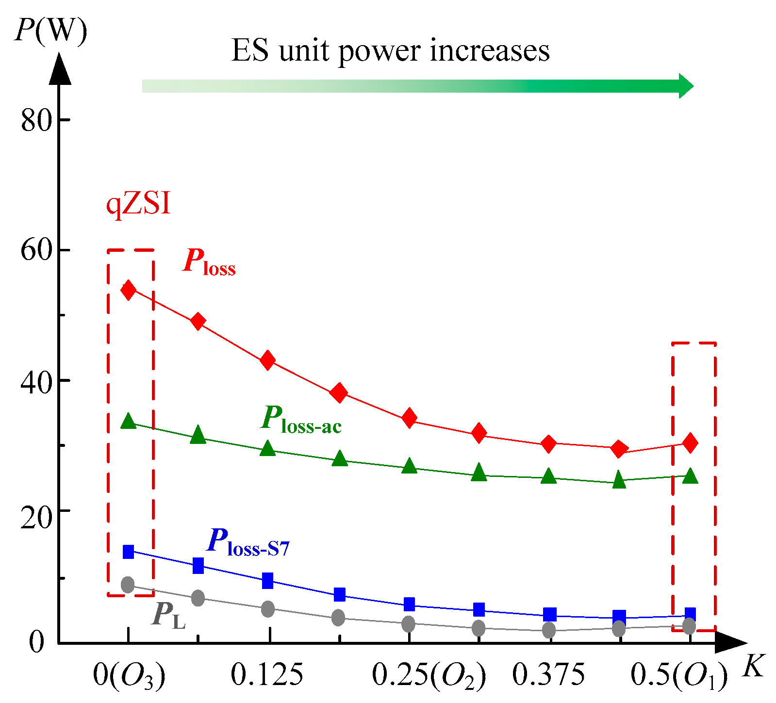
The experimental power loss profile between O1 and O3 is demonstrated in Figure 9. A low valley appears within the operation range of O1O2, verifying the analysis for profile of Ploss. From the experiment, the total power loss was reduced by up to 40% with the power distribution regulation in ES-qZSI compared with the conventional qZSI. More than 70% of reduction was provided by S7 and the passive components.
Figure 10 shows the simulation verification for the optimal energy efficiency tracking method. Initially, the system works as the conventional qZSI with K = 0. A large current value in IST can be observed. After that, the optimal energy efficiency tracking is activated and the system enters the optimal operation range. Isource2 from the energy storage units helps to reduce IST. Then, the system efficiency is improved by more than 4% through the regulation of the power distribution.
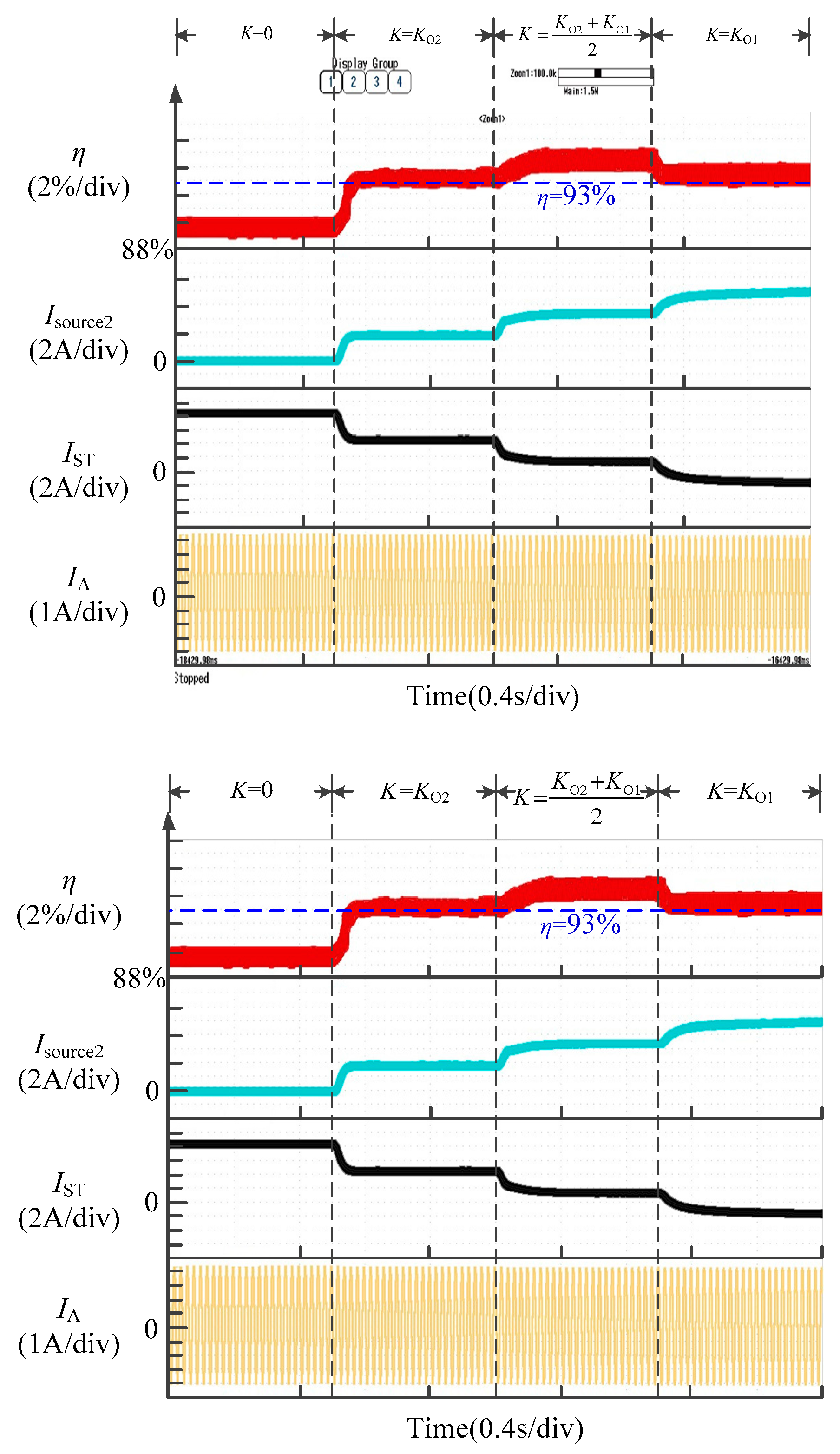
The related experimental results are shown in Figure 11. With increasing Isource2, the system efficiency increased to over 93%. Meanwhile, the shoot-through current increased up to 8 A when K = 0, which caused large current stress on S7. Through the power distribution, the ST current was reduced to nearly zero, which relieved the current stress on S7.
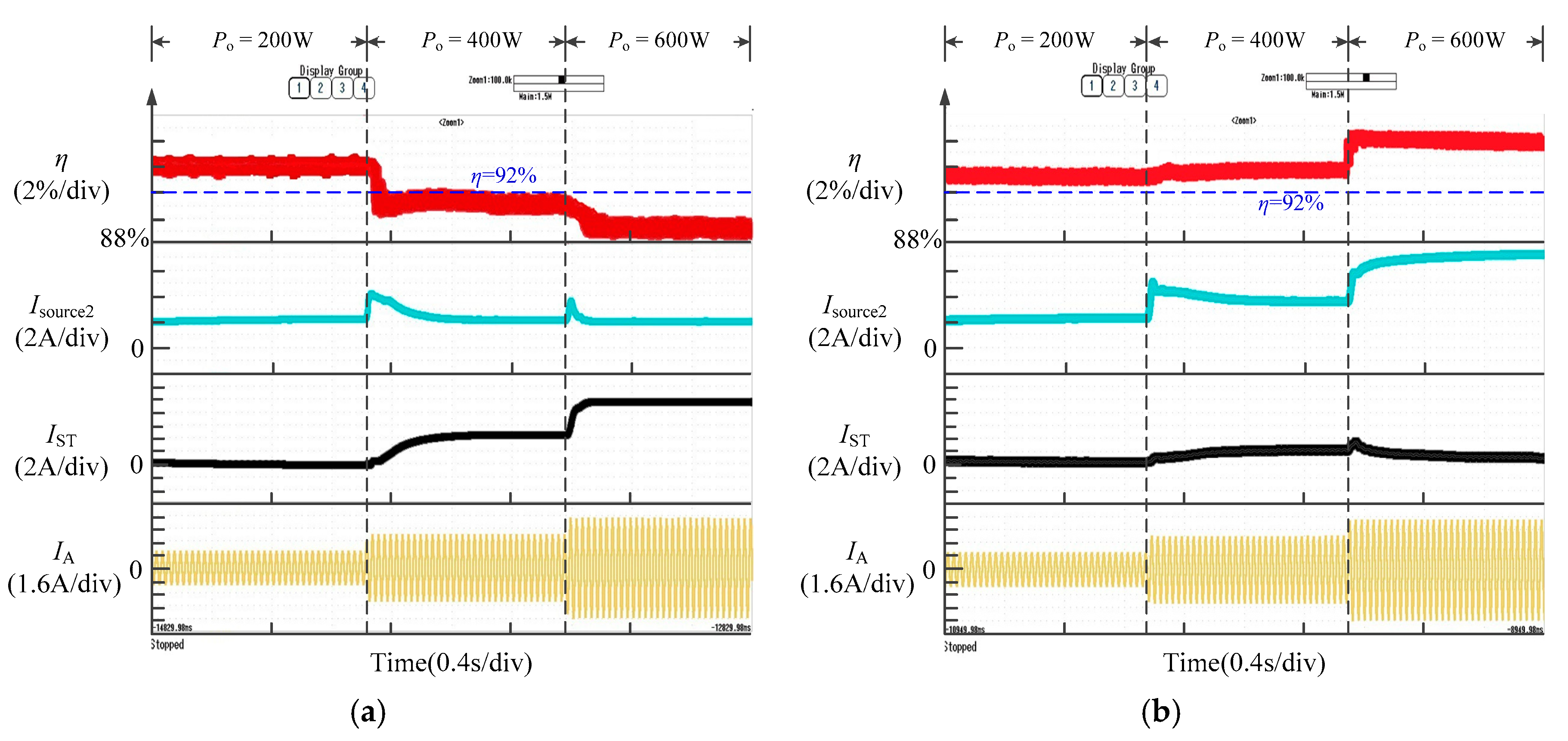
Figure 12 demonstrates the experiment waveforms to validate the optimal energy efficiency tracking method with a load power variation. In Figure 12a, the optimal energy efficiency tracking is not used and Isource2 is kept unchanged. Thus, IST increased when the load power increased, and the efficiency decreased to below 92%. In Figure 12b, Isource2 is regulated according to the optimal energy efficiency tracking method. The system operated around O1 when IST was kept at a low value during the output power variation. Then, the efficiency was maintained above 92% and the optimal energy efficiency tracking was verified.

6. Conclusions

This paper presented a detailed system power loss analysis for the ES-qZSI from the power distribution view. The current counteraction effect was studied to alleviate the device current stress. An efficiency enhancement scheme was then presented based on the quasi-inverted-trapezoidal loss profile and power distribution around the embedded energy storage units. The effectiveness of the proposed efficiency enhanced method was verified by a simulation and an experiment, resulting in a power loss decrease of over 40%. The analysis and proposed scheme may also be extended to other impedance-source-network-based energy storage systems.

Author Contributions

S.H., Z.L., and J.Z. developed the ideas of this research; Z.L. and S.H. performed the simulations and the experiments; X.Y. and S.H. revised the manuscript. All authors have read and agreed to the published version of the manuscript.

Funding

This research was funded by the National Natural Science Foundation of China (under Grant 51777188) and Grants from the Power Electronics Science and Education Development Program of Delta Environmental & Educational Foundation (DREG2019019).

Conflicts of Interest

The authors declare no conflict of interest.

Nomenclature

VbusVoltage of the DC link
Vsource1Voltage of source 1
Vsource2Voltage of source 2
Idc_linkDC-link current
IbusAverage value of DC-link current
Isource1Current of source 1
Isource2Current of source 2
DShoot-through duty ratio
ISTShoot-through current
PoOutput power
Psource1Power of source 1
Psource2Power of source 2
ηEfficiency of the system
KPower distribution ratio for source 2
IL1, IL2Current of inductors L1 and L2
BBoost ratio, Vbus/Vsource1
MModulation index
IphPeak value of the phase current
ISnCurrent of switching device Sn
IA, IB, ICPhase currents
EDiode, EIGBTSwitching energy loss of diode and IGBT (insulated gate bipolar transistor) per unit voltage and per unit current
fsSwitching frequency
E on * , E off * Energy loss during turn-on and turn-off processes from the datasheet
Vref, IrefTurn-off voltage and turn-on current in the test condition from the datasheet
I rrm * Peak value of the reverse recovery current of the diode
t rr * Reverse recovery time of the diode
Psw-S7, Pcon-S7Switching and conduction loss of DC side
Psw-ac, Pcon-acSwitching and conduction loss of AC side
fgFrequency of the grid
TsSwitching period
T1, T2Operation time for the active vectors
VCE0Forward voltage drop of IGBT or diode
ronOn resistance of IGBT or diode
rLParasitic resistance of inductors L1 and L2

Appendix A

Appendix A1. Switching Loss Derivation

The following derivation is based on the assumption that the current switching ripples are slight and can be neglected. For the DC side, two switching actions of S7 occur in one switching period with the seven-segment SVPWM (space vector pulse width modulation) algorithm. According to Equation (10) and Figure 2, IS7 switches between IST and zero when the system switches between the zero state and the ST state. Thus, the switching loss of S7 can be written as:
P sw - S 7 = { 2 f s E Diode V bus I ST I ST > 0 2 f s E IGBT V bus I ST I ST < 0
where Ediode and EIGBT are expressed as:
E IGBT = E on * + E off * V ref I ref ,   E Diode = V ref I rrm * t rr * 2 V ref I ref = I rrm * t rr * 2 I ref
For the AC side, the switching loss of all devices are the same for a balanced three-phase system. Taking S1 as an example, the switching loss can be written as:
P sw - S 1 = f g i = 1 N E IGBT V bus I A + f g i = 1 N E Diode V bus I A + 2 f g i = 0 N 1 E Diode V bus ( 1 2 I A 1 3 I ST ) + 2 f g i = N 1 + 1 N E IGBT V bus ( 1 3 I ST 1 2 I A )
The phase current in phase A can be expressed as Equation (A4). N1 represents the device current zero crossing point in ST state and is expressed as Equation (A5). Then, the switching loss on the AC side can be obtained as Equation (A6).
I A = I ph cos ( π N i + φ ) ,   N = f s 2 f g
N 1 = N π arccos 2 | I ST | 3 I ph
P sw - ac = 6 P sw - S 1

Appendix A2. Conduction Loss Derivation

The voltage drop on the switching device can be expressed as:
V on = V CE 0 + r on I on
According to Equation (10), IS7 is related to the output voltage vector. Based on the symmetry, the loss in one grid period is six times of that in one sector of the SVPWM. Here, the conduction loss in sector I (with output voltage vector 100 and 110) is shown as P’con-S7 in Equation (A8).
P con - S 7 = 6 P con - S 7 P con - S 7 = f g i = 1 N / 3 ( V CE 0 | I ST | + r on I ST 2 ) ( T s T 1 T 2 D T s ) Zero   state + f g i = 1 N / 3 [ V CE 0 | I ST I A | + r on ( I ST I A ) 2 ] T 1 Vector   100 + f g i = 1 N / 3 [ V CE 0 | I ST + I C | + r on ( I ST + I C ) 2 ] T 2 Vector   110 T 1 = M T s sin ( π 3 π N i ) ,   T 2 = M T s sin ( π N i )
The phase current in phase C is expressed as:
I C = I ph cos ( π N i + φ + 2 π 3 )
The conduction loss of the AC side are six times that of S1 with the balanced three phase-system. The conduction loss of S1 can be written as:
P con - ac = 6 P con - S 1 P con - S 1 = 2 f g i = 1 N V CE 0 | 1 2 I A 1 3 I ST | D T s + 2 f g i = 1 N r on ( 1 2 I A 1 3 I ST ) 2 D T s    + f g ( 1 D ) T s i = 1 N ( V CE 0 | I A | + r on I A 2 )
The accumulation items in Equations (A3), (A8), and (A10) are approximated by the definite integrals, and then the approximate expression of Psw-ac, Pcon-S7, and Pcon-ac can be obtained as shown in Table 1.

Appendix A3. Inductor Conduction Loss Derivation

For the inductors L1 and L2, as the ripple of inductor current is slight and neglected, the inductor loss is mainly determined by the copper DC loss, which is expressed as:
P L = r L ( I L 1 2 + I L 2 2 )
Combining Equations (3)–(5) and (A11), PL is obtained as demonstrated in Table 1.

References

  1. Xiao, J.; Wang, P.; Setyawan, L. Hierarchical control of hybrid energy storage system in DC microgrids. IEEE Trans. Ind. Electron. 2015, 62, 4915–4924. [Google Scholar] [CrossRef]
  2. Cao, J.; Emadi, A. A new battery/ultracapacitor hybrid energy storage system for electric, hybrid, and plug-in hybrid electric vehicles. IEEE Trans. Power Electron. 2012, 27, 22–132. [Google Scholar]
  3. Faisal, M.; Hannan, M.A.; Ker, P.J.; Hussain, A.; Mansor, M.B.; Blaabjerg, F. Review of energy storage system technologies in microgrid applications: Issues and challenges. IEEE Access 2018, 6, 35143–35164. [Google Scholar] [CrossRef]
  4. Wang, G.; Konstantinou, G.; Townsend, C.D.; Pou, J.; Vazquez, S.; Demetriades, G.D.; Agelidis, V.G. A review of power electronics for grid connection of utility-scale battery energy storage systems. IEEE Trans. Sustain. Energy 2016, 7, 1778–1790. [Google Scholar] [CrossRef] [Green Version]
  5. Choi, J.; Choi, I.-S.; Ahn, G.-H.; Wong, D.-J. Advanced power sharing method to improve the energy efficiency of multiple battery energy storages system. IEEE Trans. Smart Grid 2018, 9, 1292–1300. [Google Scholar] [CrossRef]
  6. Tran, D.; Khambadkone, A.M. Energy management for lifetime extension of energy storage system in micro-grid applications. IEEE Trans. Smart Grid 2013, 4, 1289–1296. [Google Scholar] [CrossRef]
  7. Dusmez, S.; Khaligh, A. A supervisory power splitting approach for a new ultracapacitor-battery vehicle deploying two propulsion machines. IEEE Trans. Ind. Informat. 2014, 10, 1960–1971. [Google Scholar] [CrossRef]
  8. Alobeidli, K.; Khadkikar, V. A new ultracapacitor state of charge control concept to enhance battery lifespan of dual storage electric vehicles. IEEE Trans. Veh. Technol. 2018, 67, 10470–10481. [Google Scholar] [CrossRef]
  9. Bilbao, E.; Barrade, P.; Etxeberria-Otadui, I.; Rufer, A.; Luri, S.; Gil, I. Optimal energy management strategy of an improved elevator with energy storage capacity based on dynamic programming. IEEE Trans. Ind. Appl. 2014, 50, 1233–1244. [Google Scholar] [CrossRef]
  10. Hu, S.; Liang, Z.; He, X. Ultracapacitor-battery hybrid energy storage system based on the asymmetric bidirectional Z-source topology for EV. IEEE Trans. Power Electron. 2016, 31, 7489–7498. [Google Scholar] [CrossRef]
  11. Liu, Y.; Ge, B.; Abu-Rub, H.; Peng, F.Z. Control system design of battery-assisted quasi-Z-source inverter for grid-tie photovoltaic power generation. IEEE Trans. Sustain. Energy 2013, 4, 994–1001. [Google Scholar] [CrossRef]
  12. Abu-Rub, H.; Iqbal, A.; Ahmed, S.M.; Li, Y.; Ge, B. Quasi-Z-source inverter-based photovoltaic generation system with maximum power tracking control using ANFIS. IEEE Trans. Sustain. Energy 2013, 4, 11–20. [Google Scholar] [CrossRef]
  13. Ge, B.; Liu, Y.; Abu-Rub, H.; Peng, F.Z. State-of-charge balancing control for a battery-energy-stored quasi-Z-source cascaded-multilevel-inverter-based photovoltaic power system. IEEE Trans. Ind. Electron. 2018, 65, 2268–2279. [Google Scholar] [CrossRef]
  14. Lashab, A.; Sera, D.; Martins, J.; Guerrero, J.M. Dual-input quasi-z-source PV inverter: Dynamic modeling, design, and control. IEEE Trans. Ind. Electron. 2020, 67, 6483–6493. [Google Scholar] [CrossRef]
  15. Abdelhakim, A.; Davari, P.; Blaabjerg, F.; Mattavelli, P. Switching loss reduction in the three-phase quasi-Z-source inverters utilizing modified space vector modulation strategies. IEEE Trans. Power Electron. 2018, 33, 4045–4060. [Google Scholar] [CrossRef] [Green Version]
  16. Liu, Y.; Ge, B.; Abu-Rub, H.; Peng, F.Z. Overview of space vector modulations for three-phase Z-source/quasi-Z-source inverters. IEEE Trans. Power Electron. 2014, 29, 2098–2108. [Google Scholar] [CrossRef]
  17. Wolski, K.; Majtczak, P.; Rabkowski, J. Minimum-hard-switching-number modulation method for high-frequency SiC-based impedance-source inverters. IEEE Trans. Ind. Electron. 2018, 65, 8351–8360. [Google Scholar] [CrossRef]
  18. Hu, S.; Liang, Z.; Fan, D.; He, X. Hybrid ultracapacitor-battery energy storage system based on quasi-Z-source topology and enhanced frequency dividing coordinated control for EV. IEEE Trans. Power Electron. 2016, 31, 7598–7610. [Google Scholar] [CrossRef]
  19. Meng, Y.; Wang, Y.; Xiong, M.; Hu, S.; He, X. power allocation for energy stored quasi-z-source inverter based on the power loss modelling. In Proceedings of the 11th Annual IEEE Energy Conversion Congress and Exposition, Baltimore, MD, USA, 29 September–3 October 2019; IEEE: Piscataway, NJ, USA, 2019; pp. 1–5. [Google Scholar]
  20. Zhou, Y.; Wu, Q.; Li, Z.; Hong, F. Research on a time-variant shoot-through modulation strategy for quasi-Z-source inverter. IEEE Trans. Power Electron. 2018, 33, 9104–9109. [Google Scholar] [CrossRef]
  21. Battiston, A.; Martin, J.; Miliani, E.; Nahid-Mobarakeh, B.; Pierfederici, S.; Meibody-Tabar, F. Comparison criteria for electric traction system using Z-source/quasi Z-source inverter and conventional architectures. IEEE J. Emerg. Sel. Top. Power Electron. 2014, 2, 467–476. [Google Scholar] [CrossRef]
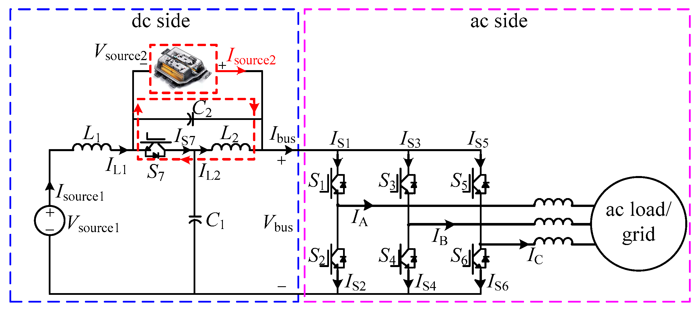
Figure 1. Current counteraction in the ES-qZSI.
Energies 13 05902 g001
Figure 2. Current commutation of the ES-qZSI and qZSI in different states: (a) ES-qZSI; (b) qZSI.
Energies 13 05902 g002
Figure 3. Power loss variation profile with respect to the shoot-through current IST.
Energies 13 05902 g003
Figure 4. Implementation of the proposed optimal energy efficiency tracking: (a) System control scheme; (b) flowchart for optimal energy efficiency tracking unit.
Energies 13 05902 g004
Figure 5. Theoretical power loss by the optimal energy efficiency tracking: (a) Po = 400 W; (b) Po = 1000 W.
Energies 13 05902 g005
Figure 6. Platform for experimental test.
Energies 13 05902 g006
Figure 7. Experimental waveform of IS7 under same output load power: (a) power distribution ratio K = 0; (b) power distribution ratio K = 0.5.
Energies 13 05902 g007
Figure 8. Experimental waveform of IS1 in ST state under same output load power: (a) Power distribution ratio K = 0; (b) Power distribution ratio K = 0.5.
Energies 13 05902 g008
Figure 9. Experimental power loss profile with respect to the power distribution ratio.
Energies 13 05902 g009
Figure 10. Simulation verification for the proposed efficiency enhancement method.
Energies 13 05902 g010
Figure 11. Experimental waveforms for the validation of the proposed efficiency enhancement method.
Energies 13 05902 g011
Figure 12. Experimental verification with load variation: (a) without and (b) with optimal energy efficiency tracking.
Energies 13 05902 g012
Table 1. Power loss of the ES-qZSI.
ItemExpressionCoefficient
Switching lossDC side P sw - S 7 = 2 α 1 f s V bus | I ST | α 1 = { E IGBT I ST < 0 E Diode I ST 0
α 2 = { E Diode I ST < 0 E IGBT I ST 0
α 3 = { E IGBT + E Diode | I ST | / I ph 1.5 0 | I ST | / I ph > 1.5
α 4 = { 2 V CE 0 | I ST | / I ph 1.5 0 | I ST | / I ph > 1.5
α 5 = { r on I ph I ST I ph   o r   I ST 0 r on I ph + V CE 0 0 < I ST < I ph
α 6 = { 3 2 M V CE 0 I ph cos φ I ST I ph 3 2 M V CE 0 I ph cos φ I ST < I ph
AC side P sw - ac = 2 α 2 f s V bus | I ST | + 6 π ( E IGBT + E Diode ) f s V bus I ph + 1 π α 3 f s V bus [ 9 I ph 2 4 I ST 2 2 | I ST | arccos 2 | I ST | 3 I ph ]
Conduction lossDC side P con - S 7 = ( 1 D ) r on I ST 2 + ( 1 D ) V CE 0 I ST 3 α 5 M I ST cos φ + M 2 π r on I ph 2 ( 3 + 2 cos 2 φ ) + α 6
AC side P con - ac = 6 ( 1 D ) π V CE 0 I ph + 6 3 D 4 r on I ph 2 + 2 D V CE 0 | I ST | + 2 3 D r on I ST 2 + 2 π α 4 D ( 9 I ph 2 4 I ST 2 2 | I ST | arccos 2 | I ST | 3 I ph )
Inductor loss P L = r L ( P o + V source 2 I ST V bus ) 2 + r L ( P o + V source 2 I ST + V source 1 I ST V bus ) 2
Table 2. System parameters of the test platform.
ItemValue
Frequency of the grid fg50 Hz
Switching frequency fs10 kHz
Voltage of source 2 Vsource250 V
Voltage of source 1 Vsource1100 V
Inductors L1, L24 mH
Capacitors C1, C2820 μF
Inductor parasitic resistance rL80 mΩ
Switching Device S1S7IKW40N120T2
Publisher’s Note: MDPI stays neutral with regard to jurisdictional claims in published maps and institutional affiliations.