Article

DGX-A100 Face to Face DGX-2—Performance, Power and Thermal Behavior Evaluation

IT4Innovations National Supercomputing Center, VŠB—Technical University of Ostrava, 708 00 Ostrava, Czech Republic
*
Author to whom correspondence should be addressed.
Energies 2021, 14(2), 376; https://doi.org/10.3390/en14020376
Submission received: 21 December 2020 / Revised: 7 January 2021 / Accepted: 8 January 2021 / Published: 12 January 2021
(This article belongs to the Special Issue Performance–Power Tradeoffs in Parallel Applications)

Abstract

:
Nvidia is a leading producer of GPUs for high-performance computing and artificial intelligence, bringing top performance and energy-efficiency. We present performance, power consumption, and thermal behavior analysis of the new Nvidia DGX-A100 server equipped with eight A100 Ampere microarchitecture GPUs. The results are compared against the previous generation of the server, Nvidia DGX-2, based on Tesla V100 GPUs. We developed a synthetic benchmark to measure the raw performance of floating-point computing units including Tensor Cores. Furthermore, thermal stability was investigated. In addition, Dynamic Frequency and Voltage Scaling (DVFS) analysis was performed to determine the best energy-efficient configuration of the GPUs executing workloads of various arithmetical intensities. Under the energy-optimal configuration the A100 GPU reaches efficiency of 51 GFLOPS/W for double-precision workload and 91 GFLOPS/W for tensor core double precision workload, which makes the A100 the most energy-efficient server accelerator for scientific simulations in the market.

1. Introduction

The modern High-Performance Computing (HPC) servers more and more often accommodate a heterogeneous hardware, which brings high computational performance hand in hand with high power efficiency in comparison to general purpose server processors [1]. Especially accelerators are considered to be a hardware platform that will enable a construction of the future exascale systems with reasonable power consumption, since their energy-efficiency is much higher when compared to general purpose server processors. The most common piece of such hardware in the list of the most powerful supercomputers nowadays are Nvidia GPUs. In November 2020, 140 of 147 accelerated systems are powered by Nvidia GPUs [2].
Besides the GPU development, in 2016, Nvidia came with the first generation of their server system called DGX-1 [3] based on their top server General Purpose GPUSs (GPGPU) with high-speed interconnect to accelerate deep learning applications. In this paper, we compare the second and the third generation of this server—DGX-2 [4] and DGX-A100 [5]. DGX-2 contains 16 Tesla V100 based on Volta architecture [6] and DGX-A100 accommodates 8 A100 GPUs based on the latest Ampere [7] architecture.
These GPUs, as well as the DGX server, not only provide high performance in half- or mixed-precision, which are the data types used in artificial intelligence (AI) applications, but also in double precision, which is required for most of the HPC workloads. In particular, the Ampere GPU comes with the first Nvidia Tensor Cores, which support double-precision computation. These Tensor Cores boost the overall 64 bit floating point performance by nearly 100% [7].
To make the DGX architecture even more interesting for data center operators, together with the DGX-A100, Nvidia came up with DGX SuperPOD platform, which is a rack of five DGX-A100, delivered in 4 up to 28 rack systems. Such a system provides massive performance. Moreover, it is deployable in weeks rather than in months with a fraction of the power consumption of a traditional supercomputer [8]. On behalf of the energy efficiency of this platform, the DGX SuperPOD composed of 140 DGX-A100 ranked as 170 in the most powerful supercomputer list Top500, and it is leading the Green500 list from November 2020 with 26.2 GFLOPS/W energy efficiency [1].
This paper is an extension to our previous conference paper [9], which presented the performance evaluation of the DGX-2. In this paper, we added the analysis of DGX-A100, and more importantly, we provide a comparison of these two flagship GPGPU servers both in terms of performance and power consumption.
The performance of these systems was evaluated using our synthetic benchmark, designed to achieve and measure the peak performance of both CPUs and GPUs, including all their vector units capabilities. For this paper, a new version of the benchmark with advanced support for Tensor Core units [10] was developed. Using the benchmark, we were able to compare our measurements to the peak performance stated by Nvidia. In addition, we measured GPU memory and NVLink throughput.
A prior research work focused on different aspects of the DGX-2 system. For instance, in Reference [11] the authors are focused on the V100 GPU architecture and explored the whole V100 memory hierarchy, including throughput and latency measurements in great details. They also inspected native Volta instructions with issue latency measurements. Furthermore, the work presented in Reference [12] focused on GPU communication technologies. It analysed aspects like throughput, latency and topology of different GPU interconnects that are used in today’s GPU servers, including the DGX-2.
In addition to the evaluation of the performance for different precisions supported by the hardware and different compute units, this paper also evaluates the thermal behavior and power consumption of both GPU architectures.
We performed Dynamic Frequency and Voltage Scaling (DVFS) [13] for compute, memory, and communication bound workloads since each of them has different hardware requirements, and identified the most energy-efficient configurations. This research follows research in DVFS on Nvidia GPUs, that has been done on Titan X [14], K20 [15], or Fermi and Maxwell [16] GPUs.
In this paper, the benchmark presented in Reference [9] is extended to support new data types introduced in Ampere GPU architecture: Bfloat on regular compute units as well as double-precision data type on the new generation of Tensor Core units. The recent GPU server from Nvidia: DGX-A100 based on the new Ampere architecture is compared with the previous generation GPU server DGX-2 based on Volta GPU architecture. The performance of floating-point units and Tensor Core units are evaluated on V100 as well as A100 GPUs for different floating point data types to verify their specification. The power consumption of these workloads is measured as well. The power throttling behavior has been examined, since it causes the down-scaling of the streaming-multiprocessor frequency resulting in performance decrease. The optimal frequency for peak energy efficiency of the new server has been identified using DVFS.

1.1. DGX-2 Platform Description

The Nvidia DGX-2 server is designed to accelerate tasks in artificial intelligence, providing a massive performance in half-precision floating-point computation: 250 TFLOPS of FP32 (float), 125 TFLOPS of FP64 (double), and 2 PFLOPS of Tensor Core FP16 (half). These values were computed from the single GPU performance multiplied by their count in the server [4,6]. In this paper the unit FLOPS refers to Floating Point Operatins Per Second. However, it is also well-suited to run any multi-GPU application. The server is composed of 16 Tesla V100-SXM3 GPUs interconnected with high speed NVLink [6]. Besides the GPUs, the DGX-2 server consists of a pair of Intel Xeon Platinum 8168 CPUs, 1.5 TB of memory, and 30 TB of fast NVMe SSD storage. The server can be equipped with either eight EDR Infiniband or 100 Gb Ethernet network cards [4]. The GPUs are spread across two trays, each containing 8 GPUs in two rows. Cooling fans are located in front of the tray as shown in Figure 1.
The Tesla V100-SXM3 GPU is equipped with 80 streaming multiprocessors (SMs) and 32 GB of HBM2 memory. Each SM consists of the following processing units: 64 FP32 (float), 64 INT32 (32 bit integer), 32 FP64 (double-precision), and 8 Tensor Cores (16 bit floating-point—half-precision) [6]. The basic operations with 16 bit floating-point data type, half-precision, are performed by FP32 floating-point units. It can also perform half2 vector operations and reach double the performance of float. In this paper, we have executed a benchmark using the vector operations.
GPUs on DGX-2 system are interconnected with hi-speed interconnect called NVLink in version 2 [6]. Single NVLink-V2 link can provide 25 GBps throughput in a single direction and 50 GBps in both directions. The system is also equipped with 12 NVSwitches. Each GPU is connected to six of these switches with a single NVLink-V2 link, providing 300 GBps bidirectional peer-to-peer (P2P) throughput [6,12].
The Volta architecture introduces Tensor Cores with 4 times higher raw compute performance compared to regular compute units in half-precision. These processing units are designed to perform fused multiply-add matrix operation D = A B + C with half precision matrices described by the tuple M × N × K , where A is an K × N matrix, B is a K × N matrix, while C and D are M × N matrices, the available tuples being .m16n16k16, .m8n32k16, and .m32n8k16 [18]. The accumulation of results can be done either in half-precision or in single-precision [10].

1.2. DGX-A100 Platform Description

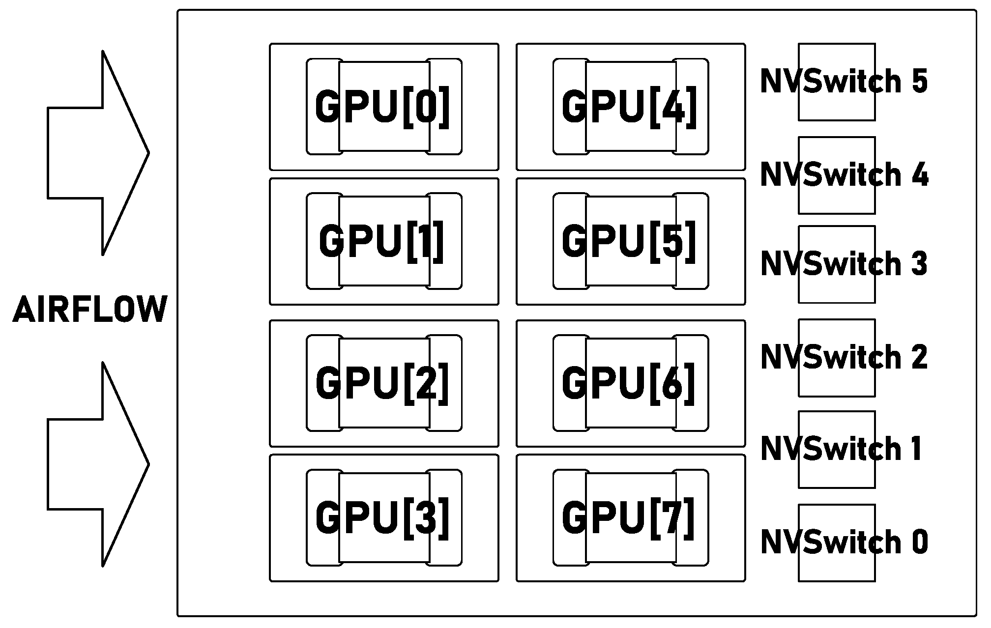
Unlike the DGX-2, its new generation, the DGX-A100 is equipped with 8 Tesla A100-SXM4 GPUs only. Altogether, these GPUs provide 156 TFLOPS of FP32, 77 TFLOPS of FP64, 156 TFLOPS of FP64 on Tensor Cores and 2.5 PFLOPS of FP16 Tensor Core performance [5,7]. The server consists of two 64 core AMD EPYC 7742 CPUs [19]. These CPUs were chosen instead of Intel Xeon CPUs because they provide PCI Express 4.0 support with more lanes. Compared to Intel CPUs, these do not have AVX-512 support, they support only AVX-2. However, they have support for PCI Express 4.0 for faster communication between CPUs and Ampere GPUs. In addition, higher energy efficiency is achieved due to TSMC’s (Taiwan Semiconductor Manufacturing Company) 7 nm fabrication process compared to Intel’s 14 nm. The server is also equipped with 1 TB of memory and 15 TB of NVMe SSD storage. Hi-speed network connectivity is provided by 200 GBps HDR Infiniband [5]. Figure 2 shows that GPUs in DGX-A100’s single GPU tray are aligned in an order different than that of the DGX-2.
The Ampere generation A100 GPU is fabricated with TSMC’s 7 nm process, compared to 12 nm process used for Volta V100 GPU. This means that A100 can fit 54.2 billion transistors in 826 mm2 die size while V100 fits only 21.1 billion transistors in 815 mm2. It uses a lower maximum frequency: 1410 MHz compared to V100’s 1597 MHz. Nevertheless, A100 incorporates more streaming multiprocessors (SMs): 108, and larger HBM2 memory: 40 GB [7]. There is also a version of A100 GPU equipped with 80 GB of HBM2e memory with higher throughput 2039 GBps [20]. In this paper, we tested the 40 GB version. Each SM of a A100 GPU contains the same number of floating-point computational units as V100’s SM: 64 FP32, 64 INT32, and 32 FP64. The difference is in the number of Tensor Cores: there are only 4 per SM but a single Tensor Core on A100 GPU has 4 times the performance of Tensor Core in V100 GPU [7].
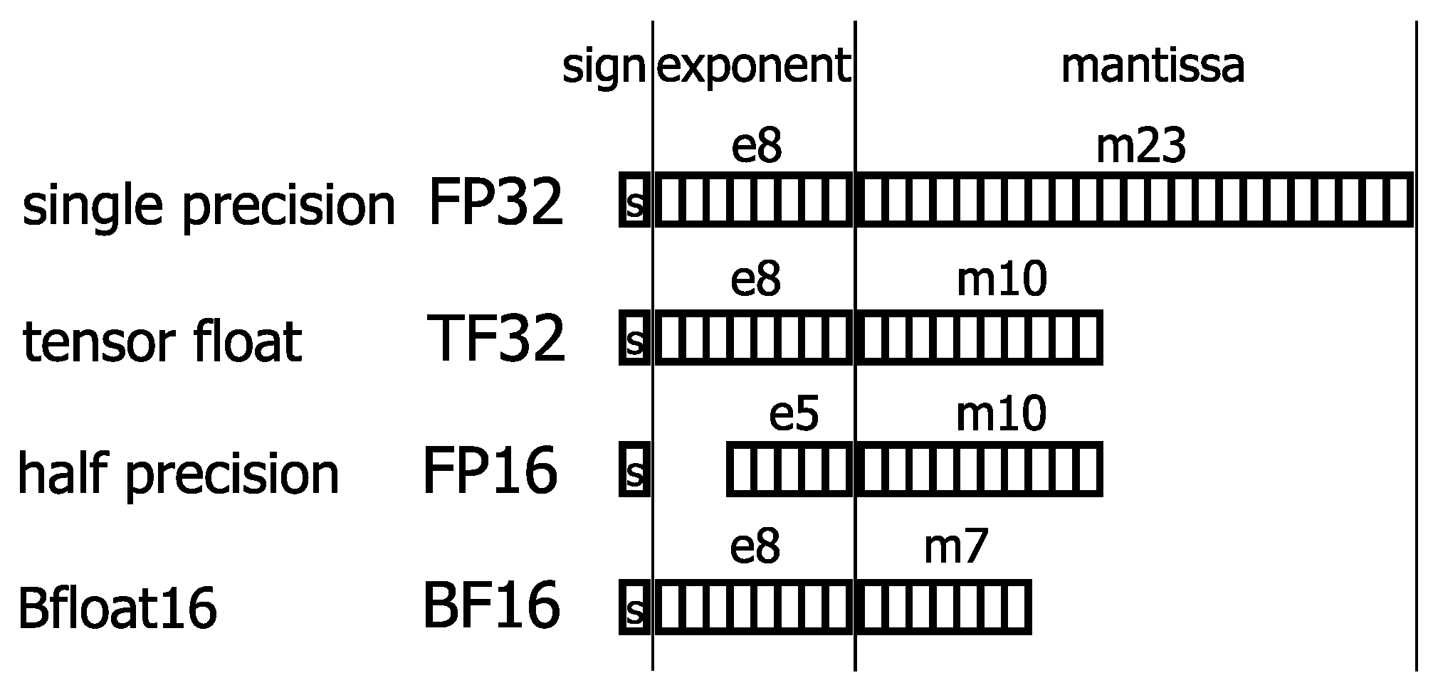
The third generation of Tensor Cores also introduced support for several new data types. Most significantly, Tensor Cores support FP64 (double-precision) computation, which makes these units more valuable for HPC. Further, data types intended for acceleration of artificial intelligence tasks are the BF16 (Bfloat16) and TF32 (tensor float). Bfloat16 is similarly to FP16 (half) stored in 16 bits, but with different arrangement. A half-precision data type is composed of 5 bits for the exponent and 10 bits for the mantissa, whereas Bfloat16 has 8 bits for the exponent and 7 bits for the mantissa. A tensor float is stored in 19 bits and keeps 8 bits for the exponent and 10 bits for the mantissa. In addition, INT8, INT4 and binary integer arithmetics is supported.
Figure 3 shows the format of these newly supported floating-point data types. All of these data types have support for matrix operations in Tensor Cores. Furthermore, Bfloat16 has additional support in regular arithmetic on single-precision compute units. Since it is 16 bits long, it supports the same vector operations as half-precision data type [7].
Ampere GPU architecture introduces a new generation of NVLink. A single link of NVLink version 3 provides similar bandwidth as the second version used in Volta: 25 GBps in single direction and 50 GBps bidirectionally. The difference is that the number of links used doubled from 6 in V100 to 12 in A100. DGX-A100 has 6 NVSwitches. Each GPU is connected to each NVSwitch with two third generation NVLinks. This means that A100 GPU achieves 300 GBps unidirectional peer-to-peer throughput and 600 GBps in both directions over NVLink [7]. Parameters of both GPU servers are compared in Table 1.

2. Measurement Methodology Description

This section describes the methodology used for both performance and energy measurements. First, the GPU implementation of our Mandelbrot benchmark is analyzed. Moreover, the necessary modifications that enable the benchmark to run on Tensor Cores are explained. Then, the tools for GPU power consumption measurement are presented together with tools for performing the DVFS. In addition, the parameters of the frequency scaling experiments are described.

2.1. Benchmarks

The Mandelbrot benchmark [9,21] is designed to measure pure floating-point performance of the processor at very high arithmetic intensity. The aim of the benchmark is to provide floating point operations load in the domain of finite numbers in the sense of IEEE 754-1975 [22], while minimizing any overheads from memory access, branching and similar. Further aim is to force floating point operations and prevent unwanted optimization, by always executing consecutive instructions with different operand. The benchmark comes in two flavors: scalar and tensor. The scalar version executes the Mandelbrot iterations z k + 1 , i = z k i 2 + c i where z 0 i = 0 and the constants c i are from the Mandelbrot set of complex numbers. The Mandelbrot iterations may be repeated indefinitely and remain bounded. For simplicity and efficiency, we select the constants c i only from the numbers on the real axis. The benchmark is implemented in CUDA PTX assembly code [18]. Each thread on the GPU device is initialized with eight unique constants c i . We use 32 threads per block and 12 blocks per streaming multiprocessor. After the initialization, all computation run in the registers only, avoiding any references to memory. The algorithm loops over k updates all values of z k i using FMA instructions. Furthermore, the loop is unrolled 100 times, counting 800 consecutive fused mulitply-add instructions, in order to out-weight the loop overhead of three instructions. The loop counter runs one million times to vastly outrun the clock granularity and provide reliable performance measurements. The measurement may be repeated number of times. The arithmetic intensity of the scalar benchmark is 12.5 × 10 6 FLOP per byte in FP64 and up to quadruple of that in FP32 and FP16 precision.
The Mandelbrot benchmark may be naturally extended to matrix domain. In matrix form, the square matrix Z is updated as Z k + 1 = Z k Z k + C , where the ∗ refers to matrix-matrix multiplication, the matrix Z 0 = 0 and the square matrix C has eigenvalues from the Mandelbrot set. Such matrix iterations may be repeated indefinitely and the matrix Z will remain bounded. It would be natural to use the matrix Mandelbrot iterations as a load to benchmark the Tensor Cores. However, the WMMA interface does not allow to insert the output of the WMMA instruction as an input into the next WMMA instruction directly due to the fact that the matrix fragments held by individual thread registers are not identical for input and output matrices.
The tensor version of benchmark executes Mandelbrot-inspired iterations of the form Z k + 1 , i = Z k i Z k i + C i , where the square matrices C i are selected such that their eigenvalues lie well within the bounds of the Mandelbrot set.
Reusing the output registers as input registers into the WMMA instruction is problematic. It can not be directly done, that is, when the accumulator and input operands are of different data type. For FP16 accumulator and input operands with shape .m16n16k16 [18], the register reuse introduces permutations into the matrix. In addition to that, some matrix elements are repeated and some are lost. For FP64 accumulator and input operands, the additional problem is that the the only available matrix shape is .m8n8k4, the accumulator and the operands are thus of different shapes: 8 × 8 for accumulator, 8 × 4 and 4 × 8 for input operands. The reuse of register introduces permutations and loss of elements into the Z k i matrix input operands.
Nevertheless, the l2 norm of the Z k i input matrices created in this way is bounded from above with respect to the source output matrix Z k 1 . The property of sub-additivity and sub-multiplicativity of the l2 norm along with selection of the C i matrices as real valued, random matrices, taken such that their eigenvalues lie well within the bounds of the Mandelbrot set allows us to establish matrix iterations that remain bounded indefinitely. Utilizing this result, the tensor Mandelbrot benchmark is implemented using the PTX WMMA instructions API [18]. The data are kept only in the registers. The matrices C i are FP16 16 × 16 matrices or FP64 8 × 8 matrices. Each block is initialized to an unique C i matrix. The C i matrices are pre-computed off the benchmark code, by shifting and scaling a randomly generated square matrices.
The block count, loop unrolling, and loop count of the tensor version benchmark remains the same as for the scalar version. The arithmetic intensity is 1.6 × 10 9 FLOP per byte for the FP16 and 1.0 × 10 8 FLOP per byte for the FP64 operations [21].
The throughput of the memory subsystem was measured by STREAM [23] benchmark, modified for GPUs, also available at the GIT repository [21]. All functions of the STREAM benchmark were measured—copy, scale, add, triadd. The throughput of the NVLink interconnect was measured by performing peer-to-peer (P2P) data transfer between two GPUs with cudaMemcpyPeerAsync() call [24]. The throughput was measured in single direction as well as bidirectionally.

2.2. Frequency Scaling and Energy Measurement Methodology

Performance of each part of a complex code is limited due to a different reason. Such kernels could be compute, memory, communication, or I/O bounded as presented in Reference [25] and further evaluated for CPU architectures in References [26,27]. Each kind of bottleneck means that other resources are not fully utilized. If the underlying hardware provides a possibility to be tuned, a resource which is not the bottleneck of the current workload can be limited without a performance penalty and also gain energy savings. Moreover, if attacking a power limit, power overprovisioning between the resources in advantage of the limiting resource may lead to improved performance [28].
Compute and memory bound workloads to evaluate the platform’s behavior including possible power and energy savings were prepared. To simulate a compute-bound workload, the Mandelbrot benchmark is used. On the other hand, memory bound workload is represented by the STREAM benchmark. Furthermore, measurement of P2P data transfer over NVLink was also performed. In this paper, the same methodology to measure energy efficiency as described in the Green500 tutorial [29] is used, the exception is that the Mandelbrot benchmark is used to determine peak performance instead of LINPACK benchmark.
When executing these workloads, DVFS is performed, using the Nvidia System Management Interface (nvidia-smi) [30]. For Volta architecture, it is possible to tune frequencies of GPU memory and streaming multiprocessors (SMs). The available SMs’ frequencies depend on the memory frequency, while for the lowest memory frequencies the upper limit of the SMs’ frequency is reduced. In comparison to server CPUs, that are usually scaled with 100 MHz step, the GPU SMs’ provide around ten times finer granularity. The GPU memory allows to set only a few frequencies. Despite that the range is quite long, and that some platforms does not allow to tune the memory frequency at all, which is the case of the tested V100 and A100 GPUs.
The frequency of V100 GPU was decreased from 1597 MHz up to 675 MHz in approximately 7 MHz predefined steps. HBM2 memory frequency cannot be tuned, thus staying at 958 MHz even when the card is idle. Since A100 GPU has lower maximum frequency, the tested range was from 1410 MHz to 690 MHz in 15 MHz steps. Memory frequency stayed at 1215 MHz.
Besides the frequency tuning, the nvidia-smi was used for power, temperature, and frequency monitoring, recorded at approximately 100 Hz sampling rate. Also, Nvidia Management Library (NVML) [31] was used for energy consumption measurement.

3. Results

The performance measurements of V100 and A100 GPUs of different data type workloads are presented in this section. The Mandelbrot benchmark described in the previous section was used for the measurements. Furthermore, the bandwidth of the GPU memory and the NVLink interconnect was measured as well. Subsequently, the power and the thermal properties of both GPU servers are also analyzed. Lastly, the DVFS was performed to find the most energy-efficient frequency for each workload type.

3.1. Performance

To the best knowledge of the authors, the peak performance numbers were not published for V100-SXM3 GPU which is used in DGX-2 server. However, the numbers were retrieved from Nvidia Profiler. The performance of Tensor Cores is not stated for this version of V100 GPU. V100-SXM2 revision has Tensor Core peak performance of 125 TFLOPS in the half-precision, running at 1530 MHz [6]. If it is scaled-up to match SXM3’s 1597 MHz, it is possible to achieve 130.484 TFLOPS in half-precision. The performance measurements of our Mandelbrot benchmark are shown in Table 2. Global memory bandwidth is according to Nvidia Profiler 980.992 GBps. Table 3 shows the bandwidth measured by STREAM benchmark. NVLink’s unidirectional P2P throughput is 150 GBps and 300 GBps in both directions and the results of our P2P benchmark are shown in Table 4.
Peak performance numbers for A100 GPU are specified in Ampere architecture whitepaper [7]. Table 2 compares the peak performance measurement to the specification. Global memory throughput of A100 GPU is 1555 GBps. The third generation of NVLink has 300 GBps unidirectional and 600 GBps bidirectional throughput. The measurement of Tensor Float and Bfloat16 on Tensor Cores is omitted because it uses type conversion before and after the computation and this does not allow data reuse within the computation, which is an essential requirements of our Mandelbrot based benchmark. The measurements were conducted on GPU rank 2 with the lowest power consumption, which is presented in the following subsection.
With the Mandelbrot benchmark, the specified performance was matched only with double data type. The performance was slightly lower than the specified performance for the other analysis. Half2 reached the peak power consumption of 410 W only for short moment and immediately lowered the frequency to 1380 MHz—this means 3% performance loss. Half on TC did not throttle the performance but the power consumption was getting close to 380 W. During this benchmark the SM utilization was at 99.52% according the Nsight Compute profiler.

3.2. Power and Thermal Properties

The cold air is not distributed equally among all the GPUs due to the physical layout of the DGX-2 server. The GPUs are placed in two trays, where each tray contains 8 GPUs in two rows. High-RPM cooling fans are located at the front of these trays. GPUs placed in the first row are facing these fans directly and receive cold air, while GPUs in the second row receive air that has been already heated by the GPUs in the first row.
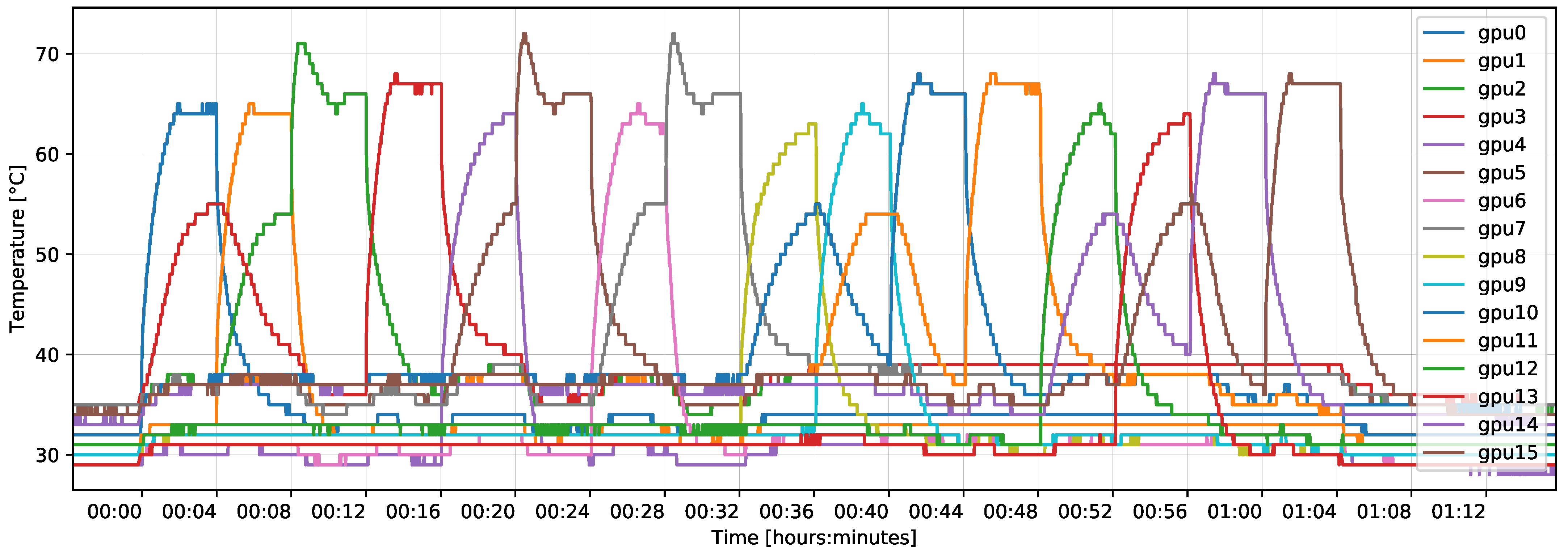
In general, this causes the GPUs in the second row to run at higher temperature than the ones in the first row. This also means that rear GPUs reach their TDP of 350 W when they are under the full load and thermal throttling must be performed, which results in performance imbalance among the GPUs. Figure 4 shows how GPUs in the first row influence GPUs in the second row by running the Mandelbrot benchmark on Tensor Cores on all 16 GPUs one after another.
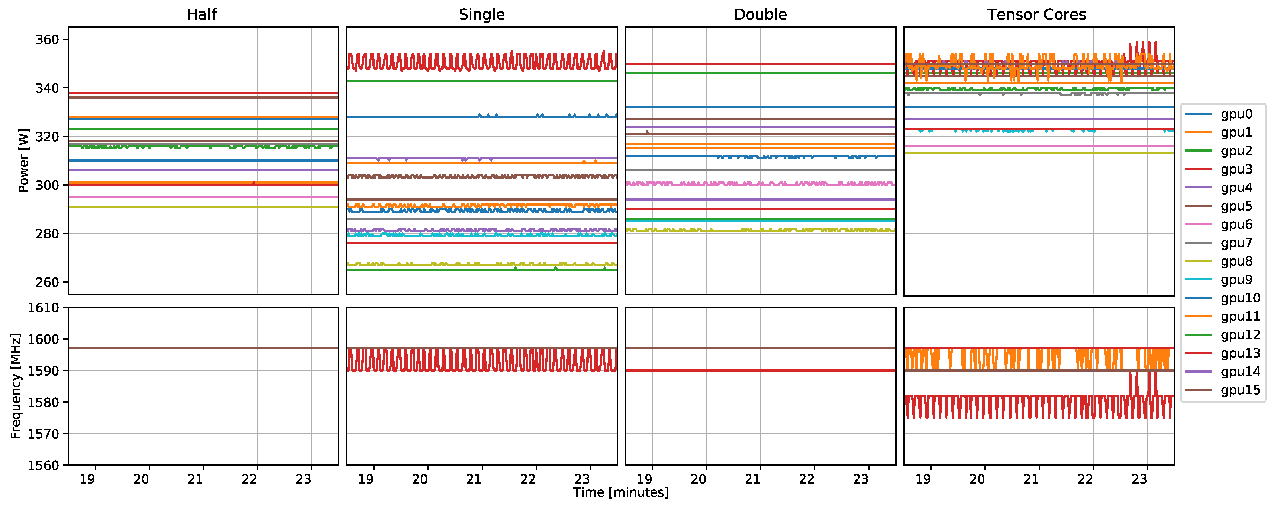
When running Tensor Core Mandelbrot benchmark on all 16 GPUs at once, GPUs in the front row reach a maximum temperature of 57 °C while GPUs in the second row peak reach 72 °C. During this benchmark, certain GPUs from the second row tend to throttle down their frequencies to as low as 1575 MHz (from the maximum 1597 MHz) causing approximately 1% performance loss, see Figure 5. It shows that running the same Mandelbrot benchmark on all the GPUs results in significant variations in power consumption of individual GPUs, reaching up to 23% for single precision version. We attribute this effect to both their location in the server, as well as their manufacturing variations. It is also observed that for single-precision, double-precision and Tensor Core version, when some GPUs reach the TDP, they under-clock their frequencies.
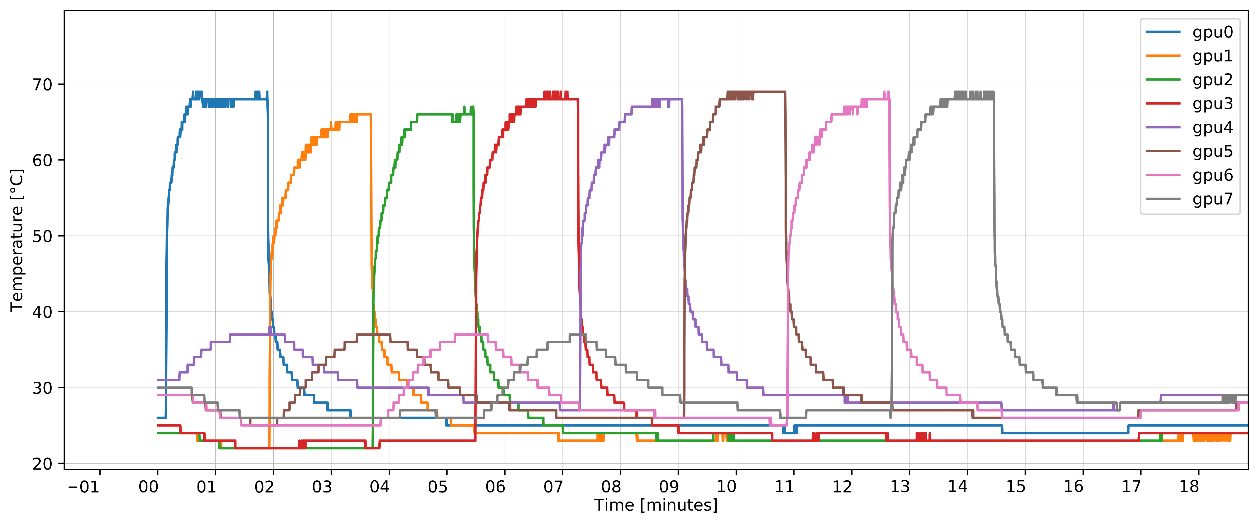
Similar to DGX-2, the DGX-A100 has GPUs placed in two rows on the GPU tray. The front row contains GPU 0–3 and the rear row has GPU 4–7. This placement is confirmed in Figure 6. It shows the temperature of GPUs when they are sequentially loaded with the Mandelbrot benchmark in half2 precision. The temperature increase of the rear GPUs is not as significant as in DGX-2 but it is still noticeable.
When all the GPUs are loaded with half2 benchmark for a time long enough to stabilize their temperatures, the temperature of GPUs in the front row peaks at 67 °C while rear row GPUs reach a maximum of 77 °C. Power consumption during this benchmark reaches the 400 W TDP limit and all GPUs underclock their frequencies. Some of them go as low as 1350 MHz. This behaviour is shown in Figure 7. It also shows that most of the GPUs reach their TDP during half benchmark on Tensor Cores. We observe underclock the frequency to as low as 1380 MHz. The A100 GPU power consumption varies within 50 W range maximum—approximately 15% for all data types of Mandelbrot benchmark.
As well as modern CPU architectures, the Nvidia GPUs support a power limiting mechanism. Well known Intel Running Average Power Limit (RAPL) [32] has a long-term power limit and a short-term power limit. In default configuration, the long-term power limit is set at approximately one second length and the Thermal Design Power (TDP) of the architecture. The short-term power limit, in default configuration is set to a fraction of a second with the power limit exceeding the TDP about extra 20%. The time windows allow the power limiting system to ignore power consumption peaks and react systematically on a power limit exceeding power requirements by reducing the frequency of the CPU, as presented in Reference [26].
The NVML provides a possibility neither to set nor to read the length of a running time window of the power limiting system. Only the power limit can be changed. As visible in the figures presenting the power consumption and the frequency of the streaming multiprocessors for V100 (Figure 5) and A100 (Figure 7), when reaching the power limit, the system reduces immediately the frequency to fulfil the power limit. Only in sporadic cases, the power consumption at the newly set frequency level results in power consumption, which the power limiting system considers as optimal. Otherwise, the frequency jitters in between two frequency levels.

3.3. Frequency Scaling

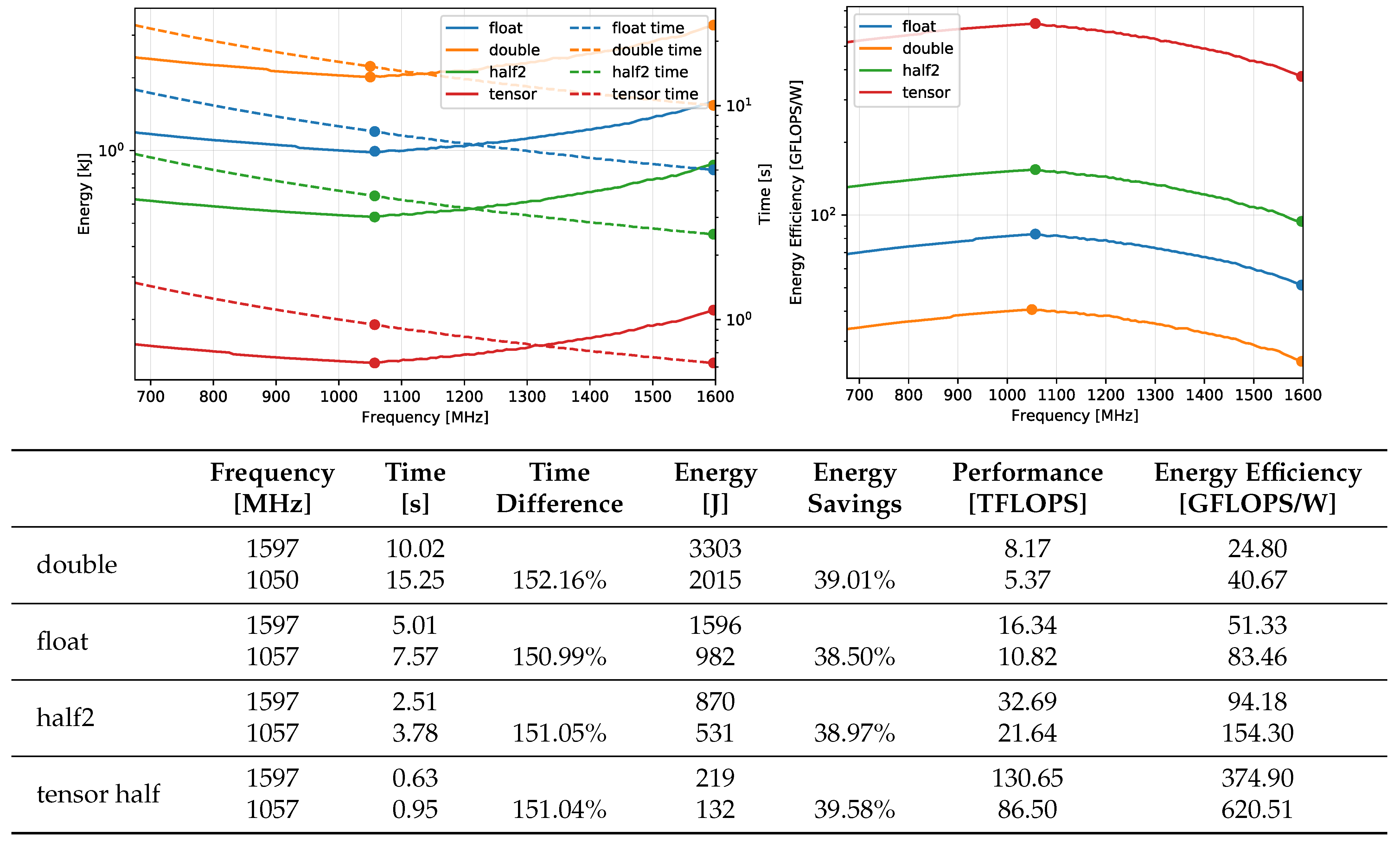
To determine whether better energy efficiency is achievable out of the evaluated GPUs, the DVFS tuning tests are performed for compute bound, memory bound, and NVLink workloads. The first frequency scaling test was performed for all the data types of the Mandelbrot benchmark (float, double, half2, tensor). The benchmark did not perform the same amount of operations. The amount of workload was adjusted according to the performance of individual compute units so that it runs approximately the same time. The results shown in Figure 8 were afterwards normalized to the same amount of work. The time and energy spent was adjusted to match 81,920 × 10 9 operations performed by benchmark in double-precision. The frequency was scaled from 1597 MHz to 675 MHz in approximately 7 MHz steps. Each frequency step was measured 6 times, and the average value is reported. The heat up runs were performed before the actual measurement.
Figure 8 shows the result of the frequency scaling. The two plots in the figure display the data in logarithmic scale. Table at the bottom of the Figure 8 compares runs at the base frequency 1597 MHz with the runs at the most energy-efficient frequency for each workload type.
In general, the most efficient frequency for compute bound workload is 1057 MHz. Running at this frequency, 39% of the energy can be saved while the run-time increases by 51%. Interesting number to point out is the energy efficiency of double data type. Running at base frequency the efficiency reaches 24.8 GFLOPS/W whereas running at 1050 MHz the efficiency reaches 40.67 GFLOPS/W. The peak performance at this frequency is only 5.37 TFLOPS, which is 66% of the original 8.17 TFLOPS. However, this efficiency number is getting close to 50 GFLOPS/W, which is the limit that was originally specified for operating a system of one exaflop peak performance with overall 20 MW power consumption [33]. This power consumption constraint had been reevaluated afterwards, while future system Aurora power consumption suppose to be around 60 MW [34].
The same measurements were done for A100-SXM4 including the newly supported data types: Bfloat16 and tensor double. The measured frequency in this case ranged from 1410 MHz to 690 MHz with 15 MHz steps. To achieve peak performance on A100 GPU, its streaming multiprocessor pipeline had to be kept full. Therefore, it was necessary to adjust the workload size for A100 GPU since it has more streaming multiprocessors than V100. The results shown in Figure 9 are normalized to match V100’s amount of workload.
The most energy-efficient frequency for A100 GPU is between 1035–1020 MHz. Depending on the data type, the achievable energy savings are in range 25–35% with 36% time increase. Although V100 can reach higher energy savings—39% the energy efficiency in the optimal frequency is 20% higher than A100 has. The performance in optimal frequency is 33% higher on A100 compared to V100. The energy-efficiency of the A100 GPU running at the maximum frequency is similar to V100’s energy efficiency running at optimal frequency for double and float datatype. On the other hand A100’s performance in optimal configuration is similar to the performance of V100 running at maximum frequency. The performance of double data type at the most energy-efficient frequency is 73% of the peak performance at the maximum frequency. In terms of energy efficiency this means 51 GFLOPS/W, which overcomes the exaflop limit. This is even more significant if double precision computations are done on Tensor Cores—91 GFLOPS/W in optimal frequency. But this is specialized hardware designed to do matrix multiplication and not general computation.
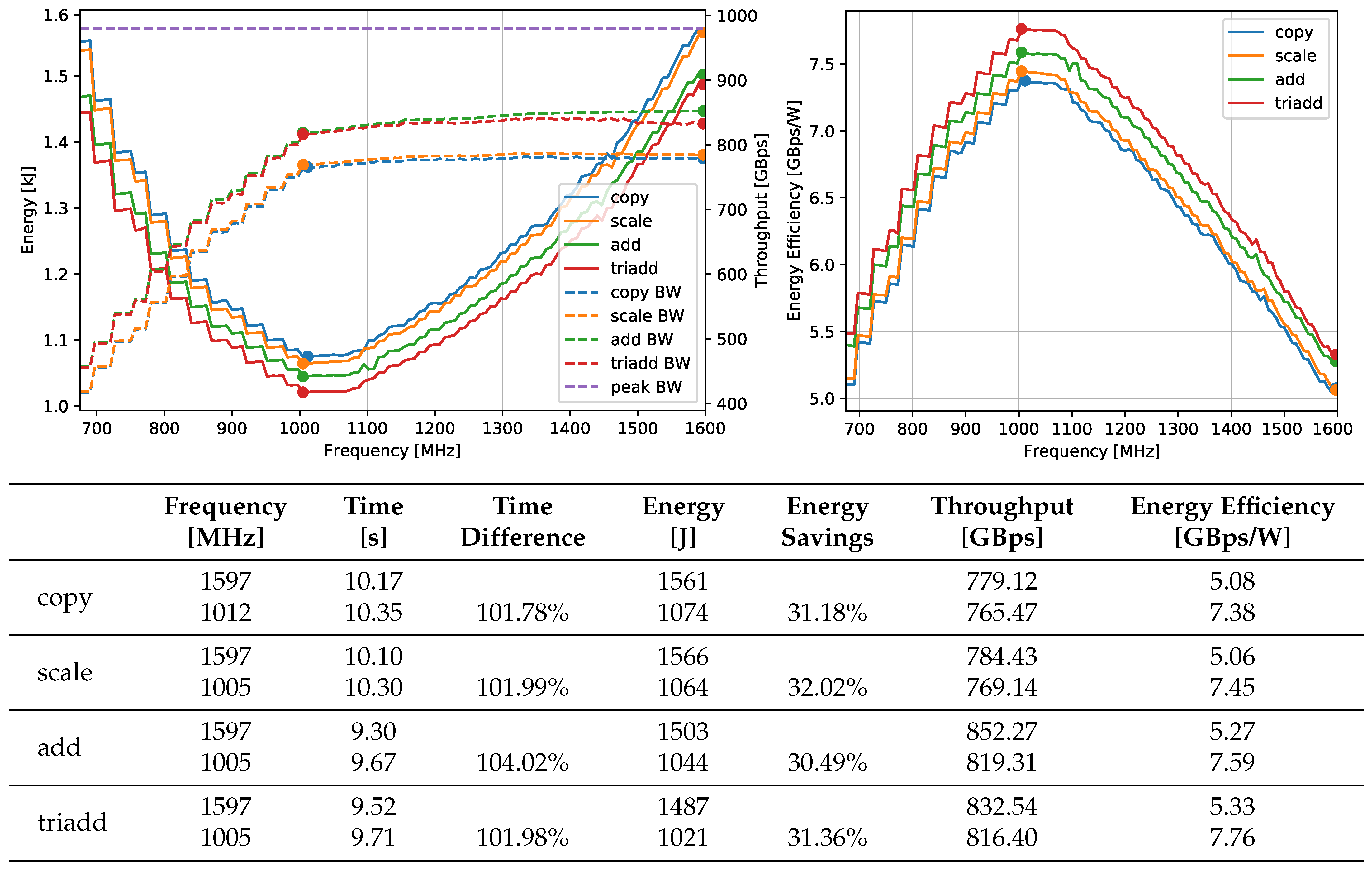
The second frequency scaling test was done using the STREAM benchmark. During this experiment, each workload transferred the same amount of data: 7.924 TB. Each frequency step was measured 6 times and average value is reported. Before the measurement started, heat up runs were performed. The frequency range and step stayed the same as during Mandelbrot benchmark on V100 GPU: from 1597 MHz to 675 MHz.
The results of the frequency scaling of the STREAM benchmark are shown in the Figure 10. The peak throughput achieved during this experiment is lower than in the Section 3.1 because the average throughput was measured and not the best case like the original STREAM does. Furthermore, the Figure 10 also shows a staircase shape when the frequency is lower than 1 GHz. This is probably caused by the GPU having certain memory operation modes. These modes do not match the granularity of which the streaming multiprocessor can change its frequency. The result of the energy consumption for base frequency and the most efficient frequency is shown in table at the bottom of the Figure 10. On average, up to 31% of the energy can be saved by scaling down to 1005 MHz. By doing that, the transfer time increased by 2%, which is almost identical in comparison to the data transfer at the base frequency.
The same experiment was also conducted for A100. Since this GPU has higher memory capacity than V100, it transfers of more data for the measurement. However, the results shown in Table at the bottom of Figure 11 were normalized to the same volume that V100 has transferred to allow direct comparison. The results are displayed in Figure 11. Significant energy decrease can be seen from the maximum frequency 1410 MHz to 1035 Mhz. The energy consumption curve then flattens from 1035 MHz lower but not completely. Therefore, in our measured frequency range 1410–690 MHz the optimal frequency for energy consumption was not found because at 690 MHz it is still slightly decreasing. The frequency 945 MHz was selected as optimal in this case because at this frequency the transfer time starts to increase, and it has the best ratio between the transfer time and energy consumed. During the frequency scaling experiment, the time of the data transfer changed only within 100 ms. The add and triadd tests run faster at optimal frequency rather than at maximum frequency.
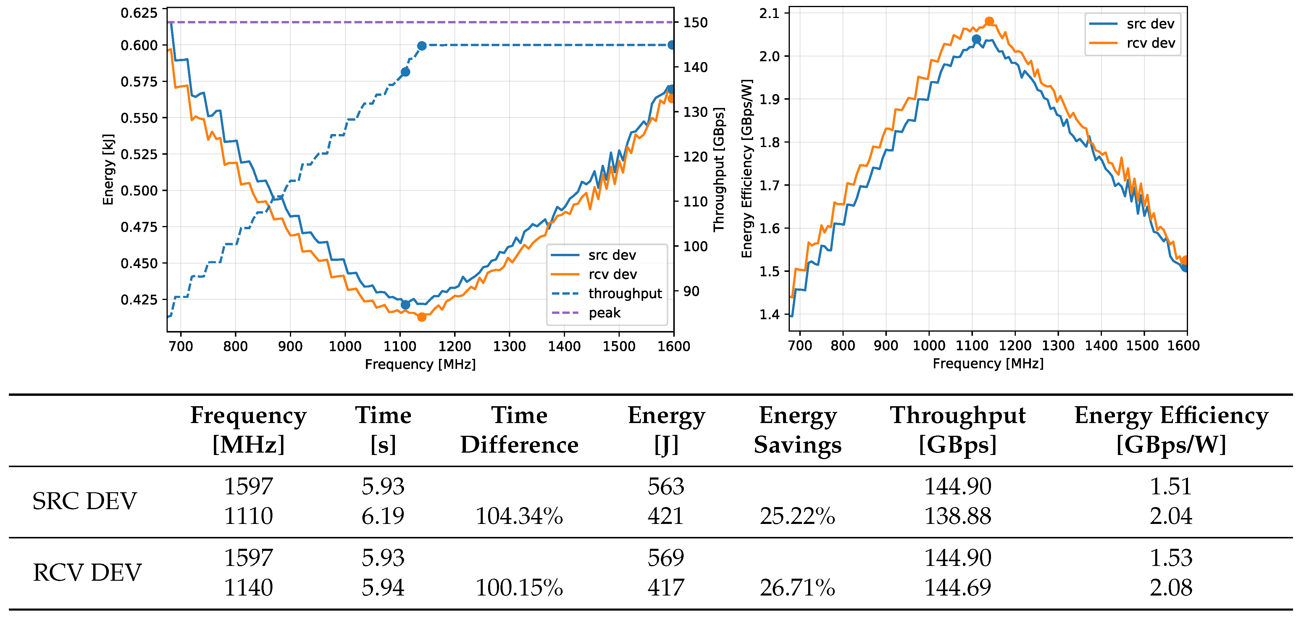
The last frequency scaling experiment was done for unidirectional P2P data transfer over NVLink. The amount of transferred data was 859 GB. One frequency step was measured 10 times. Figure 12 shows the result of this experiment. Running at 1140 MHz can save up to 26% energy without any throughput penalty. The throughput starts to drop when the frequency decreases from 1140 MHz. In addition, the staircase shape similar to Figure 10 can be seen. The table in Figure 10 shows the most efficient frequency for source and receive device and compares it to the base frequency.
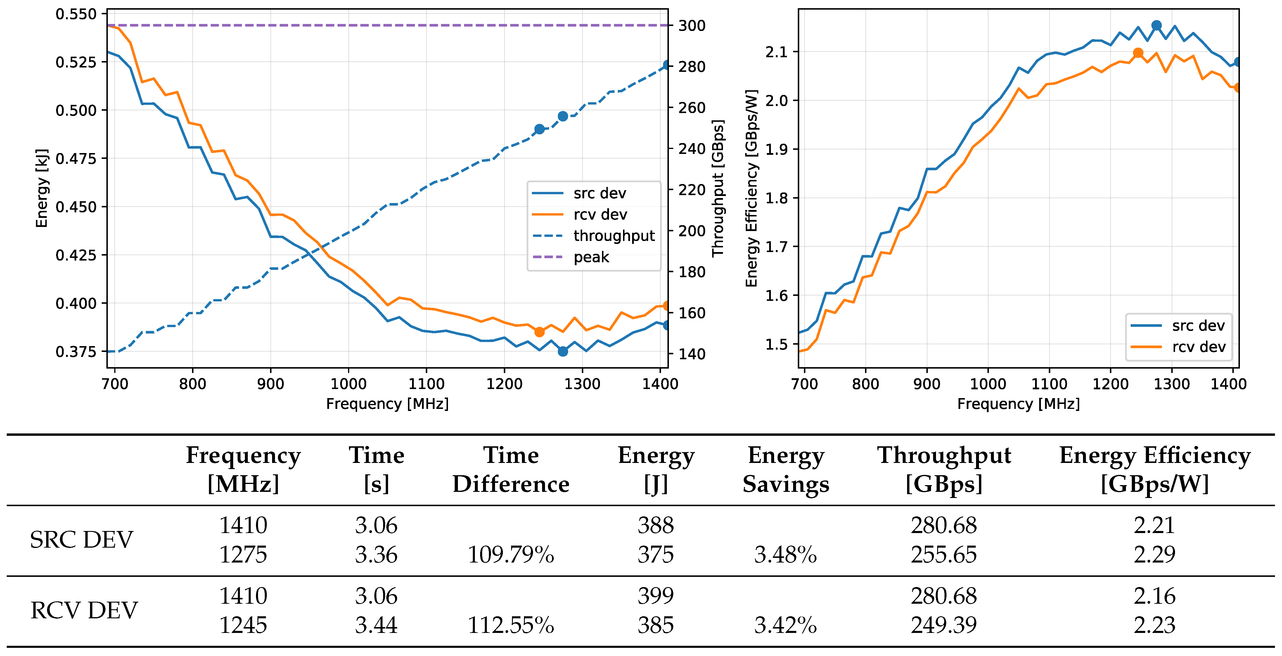
The exact same experiment was done for A100 with the same amount of data transferred. The results in Figure 13 show that the NVLink throughput drops immediately after the scaling down of the frequency is started. As a result, the optimal frequency for NVLink transfer is higher: 1275–1245 MHz. The energy savings are only 3.4% with approximately 10% throughput penalty.

4. Conclusions

The performance of floating-point units and Tensor Core units was measured on V100 as well as A100 GPUs for different floating-point data types. Our benchmarks have reached and confirmed the performance of floating point as well as Tensor Core units presented in the specification for both V100 and A100 GPUs. The power consumption of these workloads was measured as well. The A100 has the highest power consumption when it performs the computation in half-precision on regular compute units. This was the only case when we observed a power throttling due to which the streaming multiprocessor down-scaled its frequency, that caused approximately 3% performance loss. The physical layouts of the DGX-2 and DGX-A100, where the air cooled GPUs are stored in two rows, caused increased power consumption of the GPUs in the second row, which resulted in power throttling of some GPUs of DGX-2 for Tensor Core half-precision workload, and DGX-A100 half-precision tensor cores and cuda cores as well.
Our measurements identified that the power limiting mechanism of monitored GPUs is may be very unstable, causing frequent frequency changes. A CPU core frequency change is connected with a transition latency, during which the processor does not perform any computation. As future work, we plan for a deeper investigation to determine what the streaming multiprocessor transition latency is.
By using DVFS on the examined GPUs, it is possible to improve their energy efficiency. For compute bound workload on V100 it is possible to save 39% energy with 51% time increase. On A100, the same workload can save 25–35% energy depending on the data type with 36% time increase. The best generation improvement is noticeable for half-precision workload on Tensor Cores when the A100 doubled the V100’s energy efficiency from 0.62 GFLOPS/W to 1.26 GFLOPS/W.
Executing a compute bound workload for double data type at A100 in its optimal energy efficient configuration provides 20% higher energy efficiency and 33% higher performance when compared to V100’s energy-optimal frequency run. In this case, the performance of A100 in its energy-optimal frequency is getting close to the performance of V100 in its maximum frequency. The V100 reaches double-precision energy efficiency 40 GFLOPS/W. When operating the A100 GPU at its energy-optimal frequency of the streaming multiprocessors, the GPU reaches 51 GFLOPS/W in double-precision and 91 GFLOPS/W in double-precision on Tensor Cores. This implies that it is the very first server architecture that overcomes the limit of 50 GFLOPS/W, that was originally specified to build an exascale supercomputer of overall power consumption not exceeding 20 MW.
For memory bound workload on V100, it is possible to save 31% of energy and on A100 27% without a significant throughput loss. During the NVLink communication the V100 can save 25% energy without any throughput penalty. Major improvement in default energy efficiency of both V100 and A100 may be achieved by scaling down the SM frequency to approximately 1100 MHz via DVFS.

Author Contributions

Data curation, M.Š.; Investigation, M.Š. and O.V.; Methodology, L.Ř. and B.J.; Supervision, L.Ř. All authors have read and agreed to the published version of the manuscript.

Funding

This work was supported by The Ministry of Education, Youth and Sports from the Large Infrastructures for Research, Experimental Development and Innovations project “e-Infrastructure CZ–LM2018140”. This work was also partially supported by the SGC grant No. SP2020/21 “Infrastructure research and development of HPC libraries and tools II”, VŠB–Technical University of Ostrava, Czech Republic.

Institutional Review Board Statement

Not applicable.

Informed Consent Statement

Not applicable.

Data Availability Statement

The data presented in this study are openly available in the Zenodo repository at https://dx.doi.org/10.5281/zenodo.4432801, reference number [35].

Conflicts of Interest

The authors declare no conflict of interest.

References

  1. Strochmaier, E. Highlights of the 56th TOP500 List. 2020. Available online: https://sc20.supercomputing.org/presentation/?id=bof130&sess=sess314 (accessed on 4 January 2021).
  2. TOP500 List. Highlights—November 2020. 2020. Available online: https://www.top500.org/lists/top500/2020/11/highs/ (accessed on 4 January 2021).
  3. NVIDIA Corp. NVIDIA DGX-1 System Architecture White Paper. 2017. Available online: https://images.nvidia.com/content/pdf/dgx1-system-architecture-whitepaper1.pdf (accessed on 15 December 2020).
  4. NVIDIA Corp. DGX-2/2H SYSTEM User Guide. 2019. Available online: https://docs.nvidia.com/dgx/pdf/dgx2-user-guide.pdf (accessed on 15 July 2019).
  5. NVIDIA Corp. DGX A100 SYSTEM User Guide. 2020. Available online: https://docs.nvidia.com/dgx/pdf/dgxa100-user-guide.pdf (accessed on 1 December 2020).
  6. NVIDIA Corp. NVIDIA Tesla V100 GPU Architecture. 2017. Available online: http://images.nvidia.com/content/volta-architecture/pdf/volta-architecture-whitepaper.pdf (accessed on 12 July 2019).
  7. NVIDIA Corp. NVIDIA A100 Tensor Core GPU Architecture. 2020. Available online: https://www.nvidia.com/content/dam/en-zz/Solutions/Data-Center/nvidia-ampere-architecture-whitepaper.pdf (accessed on 3 December 2020).
  8. NVIDIA Corp. NVIDIA DGX SuperPOD: Scalable Infrastructure for AI Leadership. 2020. Available online: http://images.nvidia.com/aem-dam/Solutions/Data-Center/gated-resources/nvidia-dgx-superpod-a100.pdf (accessed on 11 December 2020).
  9. Spetko, M.; Riha, L.; Jansik, B. Performance, power consumption and thermal behavioral evaluation of the DGX-2 platform. In Parallel Computing: Technology Trends; IOS Press: Amsterdam, The Netherlands, 2020; Volume 36, pp. 614–623. [Google Scholar] [CrossRef]
  10. Raihan, M.A.; Goli, N.; Aamodt, T.M. Modeling Deep Learning Accelerator Enabled GPUs. In Proceedings of the 2019 IEEE International Symposium on Performance Analysis of Systems and Software (ISPASS), Madison, WI, USA, 24–26 March 2019; pp. 79–92. [Google Scholar] [CrossRef] [Green Version]
  11. Jia, Z.; Maggioni, M.; Staiger, B.; Scarpazza, D.P. Dissecting the NVIDIA Volta GPU Architecture via Microbenchmarking. arXiv 2018, arXiv:1804.06826. [Google Scholar]
  12. Li, A.; Song, S.; Chen, J.; Li, J.; Liu, X.; Tallent, N.R.; Barker, K.J. Evaluating Modern GPU Interconnect: PCIe, NVLink, NV-SLI, NVSwitch and GPUDirect. arXiv 2019, arXiv:1903.04611. [Google Scholar] [CrossRef] [Green Version]
  13. Von Kaenel, V.; Macken, P.; Degrauwe, M.G.R. A voltage reduction technique for battery-operated systems. IEEE J. Solid State Circuits 1990, 25, 1136–1140. [Google Scholar] [CrossRef]
  14. Fan, K.; Cosenza, B.; Juurlink, B. Predictable GPUs Frequency Scaling for Energy and Performance. In Proceedings of the 48th International Conference on Parallel Processing, Kyoto, Japan, 5–8 August 2019; Association for Computing Machinery: New York, NY, USA, 2019. [Google Scholar] [CrossRef] [Green Version]
  15. Ge, R.; Vogt, R.; Majumder, A.J.; Alam, M.A.U.; Burtscher, M.; Zong, Z. Effects of Dynamic Voltage and Frequency Scaling on a K20 GPU. In Proceedings of the 2013 42nd International Conference on Parallel Processing, Lyon, France, 1–4 October 2013; pp. 826–833. [Google Scholar] [CrossRef] [Green Version]
  16. Mei, X.; Wang, Q.; Chu, X. A survey and measurement study of GPU DVFS on energy conservation. Digit. Commun. Netw. 2017, 3, 89–100. [Google Scholar] [CrossRef]
  17. NVIDIA Corp. The schematic of GPU layout placed on the DGX-2 server’s chassis. Unpublished.
  18. NVIDIA Corp. Parallel Thread Execution ISA. 2019. Available online: https://docs.nvidia.com/cuda/pdf/ptx_isa_6.4.pdf (accessed on 12 July 2019).
  19. AMD Inc. AMD EPYC 7002 Series Processors Data Sheet. 2020. Available online: https://www.amd.com/system/files/documents/AMD-EPYC-7002-Series-Datasheet.pdf (accessed on 15 December 2020).
  20. NVIDIA Corp. NVIDIA A100 Tensor Core GPU. 2020. Available online: https://www.nvidia.com/content/dam/en-zz/Solutions/Data-Center/a100/pdf/a100-80gb-datasheet-update-a4-nvidia-1485612-r12-web.pdf (accessed on 1 December 2020).
  21. IT4Innovations. Mandelbrot CPU Benchmark. Available online: https://code.it4i.cz/jansik/mandelbrot. (accessed on 12 July 2019).
  22. IEEE Standard for Binary Floating-Point Arithmetic. ANSI/IEEE Std 754-1985 1985, 1–20. [CrossRef]
  23. McCalpin, J.D. Memory Bandwidth and Machine Balance in Current High Performance Computers; IEEE Computer Society Technical Committee on Computer Architecture (TCCA) Newsletter; IEEE: Piscataway, NJ, USA, 1995; pp. 19–25. [Google Scholar]
  24. NVIDIA Corp. CUDA Runtime API. 2019. Available online: https://docs.nvidia.com/pdf/CUDA_Runtime_API.pdf (accessed on 24 September 2019).
  25. Asifuzzaman, K.; Radulovic, M.; Radojkovic, P. ExaNoDe: Reporton the HPC Application Bottlenecks. Deliverable 2.5, BSC. 2017. Available online: https://exanode.eu/wp-content/uploads/2017/04/D2.5.pdf (accessed on 20 December 2020).
  26. Haidar, A.; Jagode, H.; Vaccaro, P.; YarKhan, A.; Tomov, S.; Dongarra, J. Investigating power capping toward energy-efficient scientific applications. Concurr. Comput. Pract. Exp. 2019, 31, e4485. [Google Scholar] [CrossRef]
  27. Vysocky, O.; Beseda, M.; Riha, L.; Zapletal, J.; Nikl, V.; Lysaght, M.; Kannan, V. Evaluation of the HPC Applications Dynamic Behavior in Terms of Energy Consumption. In Proceedings of the Fifth International Conference on Parallel, Distributed, Grid and Cloud Computing for Engineering, Pecs, Hungary, 30–31 May 2017; pp. 1–19, Paper 3. [Google Scholar] [CrossRef]
  28. Patki, T.; Lowenthal, D.K.; Rountree, B.; Schulz, M.; de Supinski, B.R. Exploring Hardware Overprovisioning in Power-Constrained, High Performance Computing. In Proceedings of the 27th International ACM Conference on International Conference on Supercomputing, Eugene, OR, USA, 10–14 June 2013; Association for Computing Machinery: New York, NY, USA, 2013; pp. 173–182. [Google Scholar] [CrossRef] [Green Version]
  29. Ge, R.; Feng, X.; Pyla, H.; Cameron, K.; Feng, W. Power Measurement Tutorial for the Green500 List. 2007. Available online: https://www.top500.org/files/green500/tutorial.pdf (accessed on 24 September 2019).
  30. NVIDIA Corp. Nvidia-Smi—NVIDIA System Management Interface Program. 2016. Available online: http://developer.download.nvidia.com/compute/DCGM/docs/nvidia-smi-367.38.pdf (accessed on 4 December 2020).
  31. NVIDIA Corp. NVML Reference Manual. 2019. Available online: https://docs.nvidia.com/pdf/NVML_API_Reference_Guide.pdf (accessed on 16 September 2019).
  32. Gholkar, N.; Mueller, F.; Rountree, B. Power Tuning HPC Jobs on Power-Constrained Systems. In Proceedings of the 2016 International Conference on Parallel Architectures and Compilation, Haifa, Israel, 11–15 September 2016; ACM: New York, NY, USA, 2016; pp. 179–191. [Google Scholar] [CrossRef] [Green Version]
  33. Bergman, K.; Borkar, S.; Campbell, D.; Carlson, W.; Dally, W.; Denneau, M.; Franzon, P.; Harrod, W.; Hiller, J.; Karp, S.; et al. ExaScale Computing Study: Technology Challenges in Achieving Exascale Systems. 2008. Available online: https://people.eecs.berkeley.edu/~yelick/papers/Exascale_final_report.pdf (accessed on 20 December 2020).
  34. Argonne National Laboratory. Aurora. 2020. Available online: https://www.alcf.anl.gov/aurora (accessed on 20 December 2020).
  35. Spetko, M.; Vysocky, O.; Jansik, B.; Riha, L. DGX-A100 Face to Face DGX-2—Performance, Power and Thermal Behavior Evaluation. Zenodo. 2021. Available online: https://dx.doi.org/10.5281/zenodo.4432801 (accessed on 20 December 2020).
Figure 1. Physical GPU layout of the DGX-2 server [17].
Energies 14 00376 g001
Figure 2. Physical GPU layout of the DGX-A100 server [5].
Energies 14 00376 g002
Figure 3. New data types supported in Ampere architecture [7].
Energies 14 00376 g003
Figure 4. Temperature of the DGX-2 GPUs when fully loaded with Tensor Core benchmark one after another. A GPU in the first row (0, 1, 4, 6, 8, 9, 12, 13) increases also temperature of the GPU located directly behind it in the second row (2, 3, 5, 7, 10, 11, 14, 15).
Energies 14 00376 g004
Figure 5. Power consumption variation of all the GPUs in the DGX-2 when under full load using compute bound workload with four different data-types. The variation for the single-precision workload is up to 23%.
Energies 14 00376 g005
Figure 6. Temperature of the 8 GPUs in the DGX-A100 when fully loaded with half2 benchmark one after another. A GPU in the first row (0, 1, 2, 3) increases also temperature of the GPU located directly behind it in the second row (4, 5, 6, 7). When a GPU in the second row is loaded it does not influence the temperature of any GPU in the first row.
Energies 14 00376 g006
Figure 7. Power consumption variation of all the GPUs in the DGX-A100 when under full load using compute bound workload with six different data-types.
Energies 14 00376 g007
Figure 8. DGX-2 frequency scaling of Mandelbrot benchmark. The plot in the top left corner shows consumed energy and run-time of workload. The plot in the top right corner shows energy efficiency. The plots are in logarithmic scale. The table shows the time difference, energy savings, and energy efficiency of the Mandelbrot benchmark at the base and at the optimal frequency. The marker in the plot highlights the two frequencies from the table.
Energies 14 00376 g008
Figure 9. DGX-A100 frequency scaling of Mandelbrot benchmark. The plot in the top left corner shows consumed energy and run-time of workload. The plot in the top right corner shows energy efficiency. The plots are in logarithmic scale. The table at the bottom of the figure shows the time difference, energy savings, and energy efficiency of the Mandelbrot benchmark at the base and at the optimal frequency. The marker in the plot highlights the two frequencies from the table. * During half2 test the maximum frequency 1410 MHz was not reached due to power throttling.
Energies 14 00376 g009
Figure 10. DGX-2 frequency scaling of the STREAM benchmark. The plot on the left shows consumed energy and throughput. The plot on the right shows the energy efficiency. The table at the bottom shows the time difference, energy savings, and energy efficiency of the STREAM benchmark at the base and at the optimal frequency. The marker in the plot highlights the two frequencies from the table.
Energies 14 00376 g010
Figure 11. DGX-A100 frequency scaling of the STREAM benchmark. The plot on the left shows consumed energy and throughput. The plot on the right shows the energy efficiency. The table shows the time difference, energy savings, and energy efficiency of the STREAM benchmark functions at the base and at the optimal frequency. The marker in the plot highlights the two frequencies from the table.
Energies 14 00376 g011
Figure 12. DGX-2 Frequency scaling of the NVLink P2P transfer benchmark. The plot on the left shows consumed energy and throughput. The plot on the right shows the energy efficiency. The table shows the time difference, energy savings, and energy efficiency of the NVLink transfer at the base and at the optimal frequency. The marker in the plot highlights the two frequencies from the table.
Energies 14 00376 g012
Figure 13. DGX-A100 Frequency scaling of the NVLink P2P transfer benchmark. Plot on the left shows consumed energy and throughput. Plot on the right shows the energy efficiency. The table shows the time difference, energy savings, and energy efficiency of the NVLink transfer at the base and at the optimal frequency. The marker in the plot highlights the two frequencies from the table.
Energies 14 00376 g013
Table 1. Parameters of both DGX servers. Data are collected from Nvidia Profiler and References [4,5,6,7,20].
DGX-2DGX-A100
CPU modelIntel Xeon 8168AMD EPYC 7742
PCI Express Version Support3.04.0
FP64 Performance (double)125 TFLOPS77 TFLOPS
FP32 Performance (float)250 TFLOPS156 TFLOPS
BF16 Performance (Bfloat16)312 TFLOPS
FP16 Tensor Core Performance (half)2 PFLOPS2.5 PFLOPS
TF32 Tensor Core Performance (tensor float TC)1248 TFLOPS
FP64 Tensor Core Performance (double TC)156 TFLOPS
Number of GPUs168
GPU modelV100-SXM3A100-SXM4
GPU SM/Memory Maximum Frequency1597/958 MHz1410/1215 MHz
GPU Power consumption (single GPU)350 W400 W
GPU Memory Size (single GPU)32 GB40/80 GB
GPU Memory Bandwidth (single GPU)980 GBps1555/2039 GBps
NVLink Bandwidth (bidirectional)300 GBps600 GBps
Table 2. Performance comparison V100 on the left to A100 on the right. Performance measured by Mandelbrot benchmark compared to specification.
Mandelbrot Benchmark
V100A100
Specification
[TFLOPS]
Measurement
[TFLOPS]
Specification
[TFLOPS]
Measurement
[TFLOPS]
double8.1778.1765double9.79.715
float16.35316.3530float19.519.375
half232.70732.7038half27875.654
tensor130.484130.7928half TC312310.3
Bfloat163938.752
double TC19.519.435
Table 3. V100 and A100 memory throughput measured by the STREAM benchmark compared to specification.
STREAM Benchmark Throughput [GBps]
GPUV100A100
specification980.991555.00
copy825.471329.58
scale826.521327.59
add873.631376.84
triadd872.371377.21
Table 4. P2P data transfer over NVLink interconnect parameters.
GPUV100A100
specification unidirectional150.00 GBps300.00 GBps
specification bidirectional300.00 GBps600.00 GBps
measured latency2.45 us3.65 us
measured unidirectional145.16 GBps281.00 GBps
measured bidirectional266.46 GBps531.17 GBps
Publisher’s Note: MDPI stays neutral with regard to jurisdictional claims in published maps and institutional affiliations.