1. Introduction
A fundamental understanding of the electronic and ionic transport phenomena in conjugated conducting and semiconducting polymers is of great importance and will facilitate their adoption in various device applications. The complex nanostructure of ordered crystalline areas embedded in an amorphous matrix needs to be precisely tuned and controlled to avoid the localization of charge carriers. Generally, the motion of charge carriers through the crystalline regions is faster than the amorphous areas because of the large amount of π-orbital overlap in the crystalline region [
1,
2,
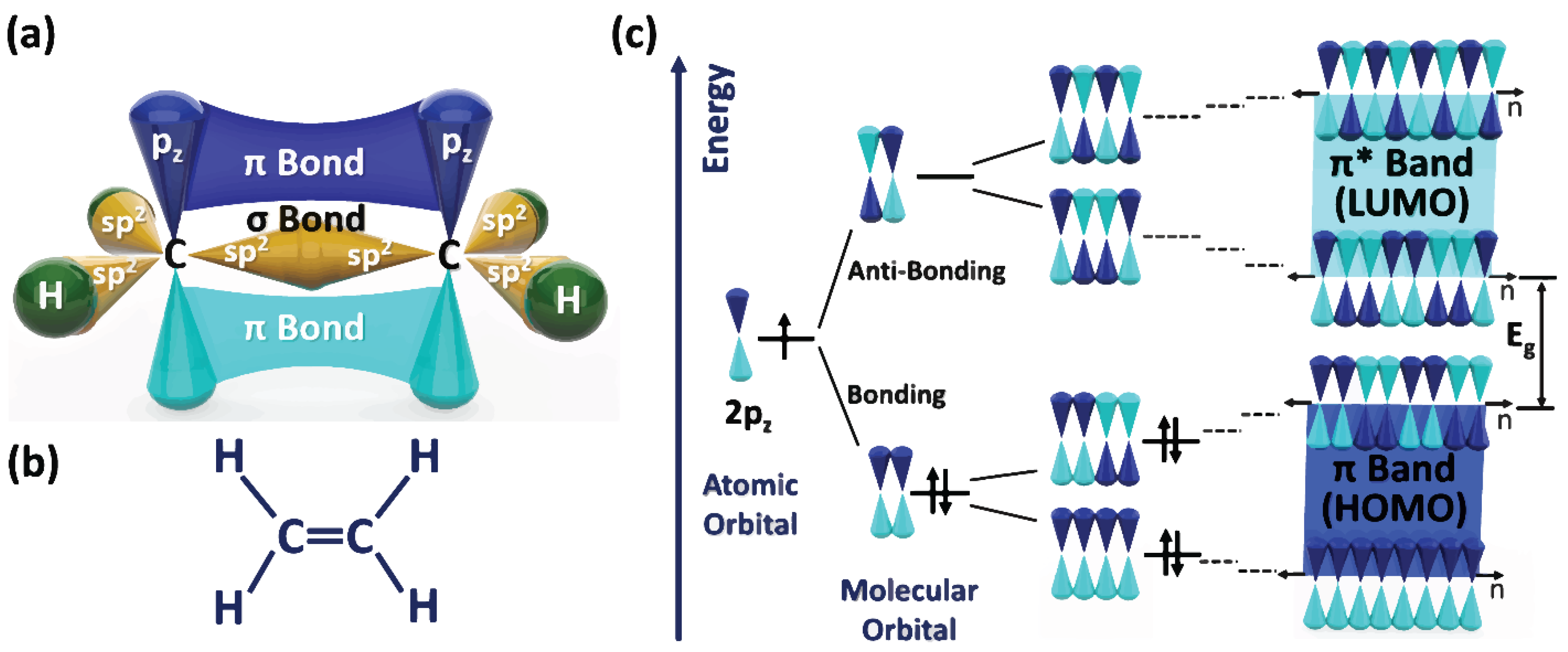
3]. Typically, there is a weak interaction of π-orbital overlap inside the amorphous regions as a consequence of the random polymer chain orientations in the amorphous areas. The backbone structure of conjugated conducting/semiconducting polymers is the source of conductivity. The backbone of conjugated conducting/semiconducting polymers is made of alternating single and double bonds. The single bond has a localized sigma (σ) integrant. In contrast, the double bond in addition to the σ integrant has a less strongly localized pi (π) component (as displayed in
Figure 1a,b) [
1].
A constituent repeat of σ and π bonded atoms along the polymer chain gives rise to the delocalization of π orbitals. The electronic interaction resulting from the movement of π-electrons along the polymer chain yields to the bonding and anti-bonding mechanism of orbitals [
1,
4,
5]. As the outcome of bonding and anti-bonding coupling between electronic and elastic properties, known as Peirerles instability, the energy level splitting of π bonds happens. As illustrated in
Figure 1c, the valence band (the highest occupied molecular orbital (HOMO)) emerges from the π band, while the conduction band (the lowest unoccupied molecular orbital (LUMO)) appears from the π* band [
1,
4,
6].
Some critical parameters of the electronic structure, such as the bandgap (
Eg), work function (
WF), Fermi level (
Ef), vacuum level energy (
Evac), ionization energy (
IE), and electron affinity (
EA), are shown in
Figure 2. These parameters need to be adjusted to optimize the device performance and generally be regulated by modifying the fabrication parameters, post-deposition, doping, and annealing steps. The bandgap (
Eg) is generally interpreted as the energy difference between the HOMO and LOMO. The work function is defined as the energy difference between the Fermi and vacuum level and displays the energy barrier for an electron to escape from a solid. The level of electrons at absolute zero is defined by the Fermi level (
Ef). The vacuum-level energy (
Evac) represents the energy level of an electron in its rest state with no kinetic energy. The energy difference between the vacuum level and the HOMO represents the ionization energy (
IE). The ionization energy refers to the minimum amount of required energy to release an electron from the top of the valence band. The electron affinity (
EA) means the obtained energy of a system by joining an electron from the vacuum level to the lowest energy level of the LUMO.
According to Mott’s theory, the extended states (known as delocalized states) are placed at the band’s center. In contrast, the localized states are situated adjacent to the band’s tails [
1]. The mobility edge (
Ec) is the critical energy at which a conversion from the localized states to the extended states occurs [
1,
7,
8]. Generally, charge carriers that have energies higher than the mobility edge play a part in conductivity, while charge carriers with energies lower than the mobility edge do not participate in conductivity. As illustrated in
Figure 2, localized states consist of shallow and deep traps. The movement of charge carriers in extended states occurs via a transport mechanism known as the band-like. In contrast, the motion of charge carriers in the shallow traps, as illustrated in
Figure 2, happens via the hopping mechanism or the multiple trapping and release (MTR) mechanism [
1]. The MTR mechanism is based on the capture of moving charges in the extended states through the existing shallow traps then the release of charges to the energy band in the pathway that is governed by a thermal activation [
1,
9].
The metallic characteristic of materials depends on the position of the Fermi level [
1,
6]. The metallic conduction behavior happens when the Fermi level passes the mobility edge and locates in the range of extended states. In contrast, materials show non-metallic conduction in the case of locating the Fermi level in localized state regions. The conduction mechanism changes from metallic to the Fermi glass insulator in the case that the Fermi level forms in the range of localized states, such as: (i) in a gap between the valence band and the bipolaron band; (ii) localized states in the polaron bands; and (iii) localized states in the band tail [
1,
10].
1.1. Homogeneous and Inhomogeneous Disorder in Conjugated Conducting Polymers
The presence of defects and disorder in conjugated polymers yields noticeable scattering of the charges and as a consequence induces the disappearance of extended states [
1,
7,
11]. Extended states are regions with mobile charge carriers and are generally formed in the middle of the HOMO or LUMO band, as shown in
Figure 2. The absence of long-distance ordering in conjugated conducting/semiconducting polymers induces a localization of the charge carriers’ wave functions, which is known as Anderson localization [
1,
7].
There are two types of disorders in conjugated polymers that are known as homogeneous disorder and inhomogeneous disorder. The type of disorder depends on the size of the crystallite domain (L
structure) and the length of the localized wave functions of the charge carrier (L
localization). The length of L
localization displays the extension of polaron/bipolaron wave functions over a stack of multiple adjacent chains [
1,
11,
12,
13,
14]. In homogeneous disorder, the crystallite domain size is smaller than the extent of the localized wave functions of the charge carrier (L
structure < L
localization). In comparison, in inhomogeneous disorder the crystallite domain size is larger than the extent of the localized wave functions of the charge carrier (L
structure > L
localization). In homogeneous disorder, the three-dimensional (3D) conductivity is reachable via an inter-chain connection [
1,
12,
13]. In contrast to inhomogeneous disorder, the conjugated conducting polymer is considered to be a combination of high-conducting crystallite regions surrounded by low-conducting amorphous areas.
The scattering of the delocalized Bloch waves in a backward manner due to the existence of defects, grain boundaries, and impurities yields the localization of charge carriers’ wave functions. Another source of the localization of charge carriers’ wave functions can be due to the passage of one-dimensional (1D) chains through areas of homogenous disorder or inhomogeneous disorder. Regardless of the localization source, the enhancement of the inter-chain charge transfer integral (through obtaining strong inter-chain coupling) is of great importance and acts as key parameter in the delocalization of charge carriers’ wave functions in homogenous or inhomogeneous disorders.
1.2. Doping in Conjugated Conducting Polymers
The doping procedure is critical to conductivity enhancement in conjugated polymers. In the case of removing an electron from the HOMO (oxidation procedure) or adding an electron to the LUMO (reduction procedure), the conjugated conducting/semiconducting polymer becomes notably conductive. The doping procedure needs the addition of a strongly oxidizing agent (p-type dopant) or a strongly reducing agent (n-type dopant). Generally, a notable fraction of the monomer units (e.g., in the range of 1/3–2/3) are doped in conjugated polymers, which corresponds to the doping concentration of 10
19–10
21 cm
−3 [
1,
11].
The optoelectronic and thermoelectric characteristics of conjugated conducting/semiconducting polymers can be tuned by controlling the dopant level. While inorganic semiconductors such as silicon have doping levels in the range of parts per billion (ppb), conjugated polymers often have doping levels in the range of one doping species per three monomers (33%) or two doping species per three monomers (66%) [
15].
Conjugated polymers are divided into the two categories of the energetically equivalent structure (degenerate ground-state) and the non-energetically equivalent structure (non-degenerate ground-state), as shown in
Figure 3a,b, respectively. The non-degeneracy of ground-state energy generally appears due to the energy difference that exists between two different structures of the conjugated polymer (known as aromatic (benzoid) and quinoid).
Generally, the charge carriers resulting from the doping procedure are often solitons in degenerate conjugated conducting or semiconducting polymers. The resulting charge carriers as a consequence of the doping procedure in non-degenerate conjugated conducting/semiconducting polymers are polarons and bipolarons. By increasing the doping level in a degenerate ground-state polymer, the number of electronic states of charged solitons increases and yields the soliton band (
Figure 3c). In non-degenerate ground-state polymers, the chain energies on either side of a defect are different. Generally, the benzoid structure (neutral structure) has less energy than the quinoid structure (oxidized structure). The movement of the soliton changes the quinoid structure to the benzoid structure and, in order to prevent this kind of change, two in-gap states between the HOMO and the LUMO are formed in non-degenerate conjugated polymers. The energy difference of chains on each side of the defect for the non-degenerate ground state yields the formation of two in-gap states (two localized electronic states) of i and i* between the HOMO and the LUMO, as illustrated in
Figure 3d,e. Polarons have a half-spin (spin of ½) and generally are established when conjugated polymers undergo a low doping level. In contrast, by increasing the doping level, two polarons would merge to form a bipolaron (which is spin-less) in order to lower the Coulombic repulsion among like charges. It is worth mentioning that the existence of a bipolaron is more common than the existence of two polarons, since the formation of a bipolaron is energetically more desirable than the creation of two polarons.
Based on the polarity of the dominant charge carrier, conjugated polymers are classified as p-type, n-type, and ambipolar (both electron and hole charge carriers). In the presence of oxidizing species (p-type dopants), the electron is extracted from the HOMO and induces a positive charge carrier along the backbone of the polymer. In the presence of reducing species (n-type dopants), an electron is added to the LUMO and yields a negative charge carrier along the polymer backbone.
Figure 4 exhibits the behavior of p-type and n-type dopants in conjugated polymers. Ionization energy (IE) and electron affinity (EA) are the key parameters for identifying p-type and n-type doping. Generally, in p-type doping, the electron affinity of the acceptor dopant is equal to or higher than the ionization energy of the polymer matrix. Therefore, in p-type doping an electron is moved from the HOMO of the organic polymer matrix and is accumulated to the LUMO of the acceptor dopant. It can be inferred that, in p-type doping, the LUMO of the dopant is placed adjacent to or below the HOMO of the polymer matrix. In contrast, in n-type doping, the HOMO of the dopant species is located adjacent to or above the LUMO of the polymer matrix, as illustrated in
Figure 4 [
1]. The most applicable and extensively studied p-type conjugated polymers are PEDOT, PANi, PPy, and PTh. The most reported n-type conjugated polymers are diketopyrrolopyrrole (DPP), naphthalene diimide (NDI), benzodifurandione-based oligo (p-phenylene vinylene) (BDOPV), isoindigo (IID), and benzothiadiazole (BT). The chemical structure of the most applicable p-type and n-type conjugated polymers are shown in
Figure 5 and
Figure 6, respectively.
For p-type conjugated conducting/semiconducting polymers, the doping efficiency enhances by an increase in the ionization energy difference of the polymer and the dopant (). The is generally called the oxidization thermodynamic deriving force. It is worth mentioning that, while p-type conjugated polymers are stable and more applicable, the high-mobility n-type conjugated polymers are rare and at the same time are unstable under atmospheric conditions and easily oxidized. In general, the development of ambient-stable n-type conjugated polymers with high mobility is challenging due to several parameters, such as (i) the scarcity of strong and stable electron-deficient monomers or building blocks with an appropriately high ionization energy and high electron affinity; and (ii) the presence of challenges and difficulties in controlling the polymerization in the electron-deficient monomer (n-type) in order to obtain a high molecular weight.
PEDOT is the most applicable conjugated polymer and upon a doping procedure with a negative counter-ion species exhibits a p-type behavior. Different kinds of counter-ions are used in PEDOT, and some of the popular ones are chloride (Cl
−), polystyrene sulfonate (PSS), and tosylate (Tos). Generally, the key variables that have an effect on the efficiency of the doping procedure in conjugated polymers with p-type characteristics are: (i) the size of the counter-ion dopant; and (ii) the difference in the electron affinities (EA) of the dopant and the ionization energy (IE) of the polymer matrix. Generally, when the doping level is higher than a certain point, the size of the counter-ion dopant is likely a critical factor [
1,
12,
16]. However, at a low doping level, the difference in the IE of the polymer matrix and the EA of the dopant is a critical variable [
16].
1.3. Semi-Crystalline Orientation of Conjugated Conducting and Semiconducting Polymers
Intermolecular forces, such as Van der Waals’ forces and hydrogen bonding, act as the key parameters in the crystallinity characteristics of conjugated polymers. Generally, the well-ordered and crystalline regions in conjugated polymers appear from the high level of π-orbital stacks. In contrast, amorphous regions emerge from weak interactions of polymer chains. The fabrication method, process parameters, size of the counter-ion dopant, size of the solubilizing side chains, variation in molecular weights, thermal annealing, and solvent treatment highly influence the crystallinity characteristics of conjugated polymers [
1]. Conjugated polymers can have a preferential texture, exhibit a mixed texture, or possess a random orientation, as shown in
Figure 7.
By considering the polymer chain as an individual lamella, there would be three possible orientations of conjugated semi-crystalline polymers, known as: face-on orientation, edge-on orientation, and end-on orientation. In the face-on texture, the conjugated backbone is parallel to the substrate, while the orientation of π-π inter-chain stacking is perpendicular to the substrate plane. In the edge-on texture, the orientation of both the conjugated backbone and π-π inter-chain stacking is parallel to the plane of the substrate. In contrast to the face-on and edge-on textures, where the conjugated backbone is parallel to the substrate, in the end-on texture the conjugated backbone is perpendicular to the substrate plane. It is worth mentioning that the appearance of the end-on texture is rare and cannot be seen frequently [
1]. A schematic illustration of the three possible textures in the case of PEDOT and P3HT are exhibited in
Figure 8 and
Figure 9, respectively.
PEDOT has a semi-crystalline characteristic and constructs in an orthorhombic unit cell, as exhibited in
Figure 10a. The PEDOT chains stack along the
b-axis lattice parameter and form in a face-to-face manner with the π-π stacking distance, which is half of the
b-axis lattice parameter (b/2). The orientation of the monomeric unit alternates by 180° along the conjugated backbone to obtain a minimum energy configuration, as shown in
Figure 10b. It is worth mentioning that the conjugated backbone of PEDOT depends upon the
c-axis lattice parameter. The
a-axis lattice parameter represents the side-to-side distance of the polymer chain. Typically, a pristine PEDOT unit cell possess lattice parameters of
a-axis, ∼14.0 Å [
17];
b-axis, ∼6.8–7.0 Å [
1,
12,
17,
18]; and
c-axis, ∼7.8 Å [
1,
11,
17].
As can be noted from
Figure 10, like PEDOT, P3HT forms and constructs in an orthorhombic unit cell, as exhibited in
Figure 10c. Typically, a pristine P3HT unit cell possesses lattice parameters of
a-axis, ∼16.8 Å;
b-axis, ∼7.6 Å; and
c-axis, ∼7.8 Å [
1,
19]. The size of the counter-ion dopant and fabrication parameters greatly affect the existing distance between polymer chains. Typically, a smaller counter-ion dopant yields improved crystallinity characteristics.
The mobility of charge carriers along the conjugated backbone generally is higher than the mobility of carriers in the perpendicular direction (direction of π-π inter-chain stacking) [
1,
11,
18]. The existence of high in-plane conductivity in comparison with the low out-of-plane electrical conductivity has been reported in PEDOT thins films [
20] as well as polyacetylene (PA) thin films such as poly(2,5-bis(3-dodecyl-2-thienyl)thieno [3,2-b]thiophene) (C12-PBTTT) and regioregular P3HT [
21].
1.4. Influence of Semi-Crystalline Orientation on the Electrical Conductivity of Conjugated Polymers
The texture and crystallization orientation of conjugated conducting/semiconducting polymers greatly affect the electrical conductivity. The most common reported textures in conducting and semiconducting polymers are the face-on texture, the edge-on texture, and a mixture of face-on and edge-on textures. High in-plane carrier mobility and conductivity have been broadly reported in conjugated conducting/semiconducting polymers with a highly face-on texture [
1,
2,
12,
15,
18,
22,
23,
24,
25,
26,
27,
28] or a highly edge-on texture [
1,
11]. In both the highly face-on texture and the highly edge-on texture, the conjugated backbone chains are formed in the plane of substrata; thus, high in-plane conductivity would be achievable. Generally, a mixture of face-on and edge-on orientations deteriorates the percolation pathways, resulting in a reduction in electrical conductivity [
1,
12,
18,
29]. It is important to note that the preferential edge-on texture is the primary texture in PEDOT:Tos, PEDOT:PSS, PEDOT:OTf, and other families of PEDOT thin films with the larger size of counter-ion dopants [
30,
31,
32,
33,
34]. The face-on texture is primarily obtained in PEDOT thin films that are synthesized with small-sized counter-ion dopants, such as chloride (Cl
−) [
12,
15,
18,
25].
The high level of in-plane conductivity in the purely face-on texture compared with other textures is ascribed to the low energy barrier of intercrystallite charge transport [
1,
2,
12,
15,
18,
25]. Poor inter-crystallite connectivity appears at high-tilt-angle grain boundaries, resulting in electrically isolated grains. Thus, a larger energy barrier for inter-crystallite transport yields a lower electrical conductivity and is expressed as [
12,
18,
35]:
where
is the electrical conductivity at different temperatures,
is the energy barrier of charge transport between crystallites, and
is the Boltzmann constant.
In conjugated conducting polymers with a highly face-on texture, particularly in a low-angle grain boundary region with the smallest amount of distortion, there is a high probability of bridging adjacent crystallites by extended polymer tie-chains [
1,
12,
18,
36]. The interconnectivity of crystallite areas expedites macroscopic charge transport, and, as a consequence, provides a pathway for electrical conduction in the disordered areas. It is assumed that a mixture of the face-on texture and the edge-on texture in conjugated polymer yields high-angle grain boundaries and provides a larger amount of misorientation among adjacent crystallites.
Figure 11 displays the impact of texture and orientation on the electrical conductivity of conjugated polymers.
1.5. Influence of Crystallite Size on the Electrical Conductivity of Conjugated Polymers
Generally, a larger crystallite size induces the enhancement of interdomain charge transport and yields an enhancement of the electrical conductivity [
1,
15,
18,
23,
31,
37,
38,
39,
40] as shown in
Figure 12. Recently, the use of water-assisted (W-A) growth in the oCVD method was developed by Heydari Gharahcheshmeh et al. [
18]. They obtained a larger crystallite size and obtained the record for electrical conductivity with the value of 7520 S/cm in a PEDOT thin film using the W-A oCVD method. It is postulated that the greater accessibility of the EDOT monomer to chloride (Cl
−) in water-assisted oCVD growth yields the formation of a crystallite with a larger size [
18].
Ugur et al. [
37] obtained an increase in the size of the PEDOT crystallite by an increase in the growth temperature, which can be controlled in the oCVD technique. Generally speaking, lowering the rate of deposition (which can be considered as the rate of polymerization) yields larger crystallites. Normally, the deposition rate (polymerization rate) of PEDOT thin films grown by the oCVD method decreases with an increase in the deposition temperature [
12,
18,
25,
37]. Gueye et al. [
31] used an N-methyl-2-pyrrolidone (NMP) additive to reduce the polymerization rate of EDOT in the solution-based method. They noted that the higher conductivity of PEDOT:Sulf-NMP in comparison with PEDOT:PSS, PEDOT:OTf, and PEDOT:OTf-NMP is mainly due to its larger crystallite size.
1.6. Inter-Chain and Intra-Chain Coupling in Conjugated Polymers
Generally, polarons and bipolarons in conjugated conducting/semiconducting polymers are localized along the chain sections. The localization of the charges on different sections of the polymer chain yields isolated energy states within the band structure and provides noncontinuous levels of electronic energy. At a high amount of doping, the wave functions of charged carriers (polaron or bipolarons) that are localized on the same chain have a tendency to overlap and provide the formation of one-dimensional intra-chain coupling [
12,
18,
24,
41]. In the same way, when the distance among different individual chains is short, there is a high probability of inter-chain coupling among adjacent localized states on each chain via the π−π stacking coupling [
12,
18].
The intra-chain coupling creates a route for the movement of localized charge carriers along the polymer backbone. In contrast, the inter-chain coupling creates a hopping path among localized coupled segments, either between two different chains or on one specific chain that is folded back on itself [
12,
18,
41]. The strong inter-chain coupling (and, thus, higher inter-chain charge transfer integral) is critical to decreasing the amount of charge localization in the presence of amorphous and defective areas in the matrix [
1,
12,
13,
18]. A schematic depicting intra-chain and inter-chain couplings in conjugated conducting/semiconducting polymers is exhibited in
Figure 13a,b. In the case of strong inter-chain coupling in highly doped conjugated conducting/semiconducting polymers, through reducing the
b-axis lattice parameter (correlated to the decrease in the π-π stacking distance), there is a high chance that an electron can move and diffuse to an adjacent chain. In such a string of inter-chain couplings in highly-doped conjugated conducting polymers, the states of electrons are extended three-dimensionally, and conducting polymers display metallic behavior [
12,
18].
1.7. Effect of Inter-Chain Coupling and Charge Transfer Integral on Electrical Conductivity
The in-plane conduction in conjugated conducting/semiconducting polymers is greatly affected by the transport of current along the lamella structure of polymer chains. The inter-crystallite coupling made by straight-tie chains would be expected to increase the mobility of charge carriers along the extended backbone of polymer chains. A strong inter-chain coupling in conjugated conducting/semiconducting polymers is an important parameter to avoid the localization of charge carriers in disordered and amorphous areas. Generally, high conductivity can be achieved in conjugated polymers by decreasing the π-π stacking distance, as displayed in
Figure 14.
In addition to conjugated polymers, the importance of inter-chain coupling has also often been noted in other organic conductor materials, such as organic superconductors. It is worth mentioning that the first reported superconductivity behavior in organic materials is related to the Di(2,3,6,7-tetramethyl-1,4,5,8-tetraselenafulvalenium) Hexafluorophosphate ((TMTSF)
2PF
6) and was achieved by reducing the inter-chain distance via using an external pressure [
42]. The importance of strong inter-chain coupling was recently reported in PEDOT [
12,
18,
28,
33,
34], P3HT [
3,
43], and a diketopyrrolopyrrole (DPP)-based conjugated donor–acceptor polymer [
41].
The charge transfer integral describes the robustness of an electronic coupling and is greatly affected by inter-chain or inter-molecular stacking. An increase in the inter-chain charge transfer integral (
) is a key variable to enhance the electrical conduction. The inter-chain charge transfer integral displays an exponential reduction as a function of the inter-chain distance and is described as [
1,
12,
18]:
where
stands for the charge transfer integral when the distance between polymer chains is at its minimum value,
is the distance among polymer chains, and 1/
is the wave function overlap decay length.
The charge transfer rate (
) is expressed by the semi-classical Marcus–Hush theory, has a direct relationship with the square of the inter-chain charge transfer integral (
), and is described as [
1,
18,
44,
45]:
where
is the charge transfer rate among the initial and final states,
is the Planck constant,
is the Boltzmann constant,
is the energy difference among the initial and final electronic states on nearby chains,
is the temperature, and
is the charge carrier reorganization energy, which is related to the rearrangement of molecules and their surroundings during a charge transfer.
The expression in Equation (3) can be used in the Einstein equation to determine the charge carrier mobility due to chain-to-chain coupling, known as
μcc, which is expressed as [
1,
18]:
where
is the electronic charge,
is the charge diffusion coefficient and is given by (
),
is the number of integers and represents the system’s dimensionality,
is the center-to-center mass distance to neighbor
, and
is the relative diffusion probability to the
th neighbor.
A reduction in the π-π stacking distance from 3.50 Å to 3.43 Å in PEDOT thin films fabricated by the oxidative chemical vapor deposition (oCVD) method yielded the record for electrical conductivity of 7520 ± 240 S cm
−1 [
18]. π-π stacking with a short distance is achievable in the oCVD method via adjusting the fabrication parameter known as the oxidant saturation ratio (OSR) [
12,
18]. The OSR is an important parameter in the oCVD technique and greatly affects the lattice parameter and π-π stacking distance, as shown in
Figure 15. A reduction in the π-π stacking distance is achievable via tuning the OSR in the oCVD method, while in solution-based methods the modification of PEDOT:PSS solution by the addition of polar solvents and ionic species is a suitable approach to reducing the π-π stacking distance [
13,
33,
34,
46].
The importance of strong inter-chain coupling to increasing the value of the inter-chain charge transfer integral and as a consequence achieving a high in-plane conductivity has also been noted in other conjugated conducting/semiconducting polymers, such as P3HT [
3,
21,
47]. In the majority of conjugated conducting/semiconducting polymers, the movement of the charge carrier along the conjugated backbone (intra-chain transport) is much faster than inter-chain transport. In both a highly face-on orientation and a highly edge-on texture, the conjugated backbone polymer chain is formed in the plane of the thin film. In general, high in-plane electrical conduction is achievable in conjugated conducting/semiconducting polymers with a highly face-on orientation or a highly edge-on orientation.
Obtaining π-π stacking with a short distance through tuning and adjusting the fabrication parameters and a post-treatment approach is a suitable way to improve the in-plane electrical conductivity in conjugated polymers with a highly face-on texture or with a highly edge-on texture [
1,
11,
18]. A mixture of face-on and edge-on orientations yields low electrical conductivity. The strong inter-chain coupling due to the short distance of π-π stacking induces an improvement in the inter-chain charge transfer integral and creates a bypass to overcome the charge localization in conjugated polymers.
Figure 16a,b exhibit the possible current transfer mechanisms among crystallites in the case of the presence of tie chains and a short π-π stacking distance in conjugated conducting/semiconducting polymers with highly face-on and highly edge-on orientations, respectively.
Generally, high in-plane electrical conduction can be obtained in the case of quasi-1D conductivity. High electrical conductivity can be achieved in conjugated conducting/semiconducting polymers under the following conditions [
1]:
- (i)
Short π-π stacking distances (a high inter-chain charge transfer integral to avoid charge localization);
- (ii)
Planarity of the backbone;
- (iii)
A highly face-on texture or a highly edge-on texture, which yields a better percolation pathway (no orientation anisotropy due to the mixed orientation) and also yields more tie chains;
- (iv)
A large crystallite size;
- (v)
The fabrication of ultrathin or fiber-like conjugated polymers.
1.8. Charge Transport Mechanisms in Conjugated Conducting/Semiconducting Polymers
Conjugated polymers exhibit different morphological characteristics as a consequence of spatial disorders distributed in the polymer matrix, as shown in
Figure 17. Various charge transport mechanisms are expected in conjugated polymers, depending on the localized and extended states [
11]. Presented models of electronic transport in conjugated polymers must consider the fact that localized states appear only at specific locations. Thus, models of electronic transport must consider spatial disorders in the crystalline and amorphous regions at the macromolecule levels, where intra-chain and inter-chain transport are different. Based on the specific morphological characteristics of conjugated polymers (
Figure 12), multiple charge transport mechanisms and models can be applied.
Group I models are related to conjugated polymers with a partial localization of extended states and start by considering the fact that states are fully extended over the entire polymer thin film. In this model, the presence of disorders and defects yields the localization of charge carriers. This procedure is frequently applied to crystalline conjugated polymers and transparent conducting oxides (TCOs) such as indium tin oxide (ITO), aluminum-doped zinc oxide (AZO), and fluorine-doped tin oxide (FTO). The models that are frequently used for Group I include Drude theory [
1,
11,
35,
48], Brook–Herring–Dingle (BHD) theory [
1,
49,
50], Seto’s model [
11,
51], inter-chain coupling due to π-π stacking [
1,
11,
12,
13,
18], and Marcus–Hush theory [
1,
44,
45].
Group II models are related to conjugated polymers with a partial delocalization of molecular orbitals and begin from the localized molecular orbitals of the polymer chains. The existence of interactions among individual chains yields delocalization of the wave functions. Typically, π-π stacking is often the strongest form of inter-molecular interaction between electronic orbitals in conjugated polymers. Any torsional change along the backbone due to the defects disrupts the conjugation, breaking it into multiple subunits. A charge transfer between the conjugated segments can generally happen through inter- and intra-chain hopping. The models that are frequently used for Group II include Mott’s variable range hopping (VRH) theory [
1,
11,
15,
37,
52,
53], the Miller–Abrahams model [
1,
54,
55], the Efros–Shklovskii (ES) VRH model [
1,
56,
57], the gaussian disorder model (GDM) [
1,
11,
58,
59,
60], inter-chain coupling due to π-π stacking [
1,
11,
12,
13,
18], and multiple trapping and release (MTR) [
1,
11,
61].
Group III models are related to conjugated polymers with semi-crystalline characteristics as a mixture of ordered and disordered regions with partial delocalization due to ordered domains. For the ordered crystalline regions, coarse-grained models consider states that fully extend over the nano-crystallites but that extend into the surrounding amorphous areas to a limited degree. Group III models are appropriate when inter-crystallite transport limits the overall mobility of the charge carrier. With precise control over morphology, the inter-crystalline charge barrier can be reduced. In this case, when the semi-crystalline characteristics exhibit a preferential texture, as a consequence of advanced control over morphology, Group I models become more appropriate. As shown in
Figure 17, semi-crystalline conjugated polymers with a preferential texture can be considered in Group I models. The models that are frequently used for Group III include course-grained VRH [
1,
11,
37], inter-chain coupling due to π-π stacking [
1,
11,
12,
13,
18], and fluctuation-induced tunneling (FIT) [
1,
62].
Figure 18 shows a schematic illustration of inter-crystallite and inter-chain charge transport rates. Generally, adjusting the fabrication parameters and using post-processing procedures will improve the crystallinity characteristics and induce the enhancement of inter-crystalline charge transport. However, the key parameter that affects the rate of charge carrier transport is the strong inter-chain coupling achieved by reducing the π-π stacking distance. The rate of charge carrier transport depends mainly on the π-π stacking distance and is higher for a short distance. Increasing the inter-chain charge transfer integral through a reduction in the π-π stacking distance is a promising procedure for enhancing the electrical conductivity in conjugated conducting/semiconducting polymers. Generally, the total rate of inter-crystallite and inter-chain charge carrier transport will be determined by the slower of the two processes occurring in series. Modifying the overall rate requires reducing the amount of disorder so that the inter-crystallite transport is not rate-limiting, i.e., moving from a low-order region (Group II) to a high-order region (Group I), as exhibited in
Figure 18.
2. Optoelectronic Properties of Conjugated Polymers
Conjugated polymers have attracted a tremendous amount of attention in optoelectronic devices. For solar cell devices and light-emitting diodes, conjugated conducting/semiconducting polymers have been widely studied as transparent conducting electrodes (TCEs), hole transport layers (HTLs), and semi-conductive active layers. Conjugated conducting/semiconducting polymers have also attracted attention for use as flexible and crack-resistant TCEs for touchscreen devices.
Transparent conductive oxides (TCOs), such as indium tin oxide (ITO), aluminum-doped zinc oxide (AZO), and fluorine-doped tin oxide (FTO), are extensively used as TCEs in optoelectronic devices. The brittleness, high cost, and scarcity of raw materials for TCOs makes them more challenging to use in flexible electronic devices. The figure of merit (FoM), which is known as the ratio of the DC conductivity (σ
dc) to the optical conductivity (σ
op), is an indication of TCE performance. The FoM can be calculated and extracted according to the following equation [
1,
11,
12,
18,
28]:
where
T(
λ) is the measured value of transmittance at the optical frequency of
λ (most commonly,
λ is the visible wavelength of 550 nm),
Z0 = 377 Ω is the free space impedance, and
Rsh is the resistance of the sheet.
Desirable and modified TCE candidates need to have FoM values >35. For PEDOT:Cl fabricated by oxidative chemical vapor deposition (oCVD), FoM values in the range of 90–94 have been reported recently [
18]. A summary of recent developments in TCEs with a focus on the FoM values is reported in
Figure 19 for PEDOT, graphene, graphene oxide, carbon nanotubes, metal nanowires, and their composites [
1].
Conjugated conducting and semiconducting polymers have attracted a tremendous amount of attention for the fabrication of electronic devices over large areas and onto flexible substrates. Some of the electronic devices based on the integration of conducting polymers are exhibited in
Figure 20. In organic polymeric optoelectronic materials, as well as small conjugated molecules, the π-π stacking motifs control the exciton delocalization and transport mechanism. The areas that consist of conjugation are referred to as chromophores. Aggregates of small conjugated molecules regulate their photophysics [
11]. Generally, a face-to-face arrangement yields an inter-chain coupling and is known as an H-aggregate. In contrast, the side-by-side packing of conjugation regions occurs for an intra-chain coupling and is known as a J-aggregate [
11].
Photovoltaic devices need one or more TCEs through which light can penetrate and strike a photoactive layer to generate electricity. TCEs based on conducting polymers, compared with ITO (ITO is a commonly used material for TCEs), have the advantages of a low cost, a low fabrication temperature, flexibility, scalability in large areas, and the capability to be used with lightweight substrates. Recently, the integration of optimized PEDOT thin films grown by oxidative chemical vapor deposition (oCVD) as a hole transport layer (HTL) was demonstrated in an inverted perovskite solar cell (PSC), as exhibited in
Figure 21 [
12]. Heydari Gharahcheshmeh et al. [
12] obtained a power conversion efficiency (PCE) of 18.04% in a perovskite solar cell (PSC) based on oCVD PEDOT as an HTL, which was higher than the PCE of 16.20% for the control PSC with a spun-cast PEDOT:PSS. More significantly, they noticed that incorporating oCVD PEDOT, rather than PEDOT:PSS, increased the device’s shelf-life stability by approximately two-fold over a 42-day evaluation period [
12]. The PCE deterioration in a PSC with PEDOT:PSS as an HTL is mainly attributed to the degradation of the perovskite material due to the highly acidic nature of PEDOT:PSS [
12]. The substitution of PEDOT:PSS with a more stable HTL, e.g., PEDOT:Cl, can resolve the stability issue and dramatically enhance the stability of PSC devices [
12].
While oCVD is an excellent technique for the growth of high-quality conducting polymer thin films, there is much ongoing research on a solution-based process with an emphasis on PEDOT:PSS as a hole transfer layer (HTL) in organic solar cells, perovskite solar cells, and quantum-dot solar cell devices. Jeng et al. [
63] reported a PCE of 3.9% in a CH
3NH
3PbI
3 (known as methylammonium lead triiodide (MAPbI
3)) perovskite thin film grown by spin-coating from a dimethylformamide (DMF) solution while using PEDOT:PSS as the HTL. They used an ITO/PEDOT:PSS/Planar Heterojunction (made of CH
3NH
3PbI
3 as the donor and C60 as the acceptor)/BCP/Al device structure [
63]. Xu et al. [
64] fabricated lead sulfide (PbS) quantum dot (QD) solar cells in an inverted structure while using PEDOT:PSS as the anode buffer layer and obtained a PCE value of 4.1%. They investigated three different anode buffer layers (PEDOT:PSS, NiO, and V
2O
5) while using a fixed cathode of PCBM and noticed that the low-temperature-processed PEDOT:PSS film yielded a smooth film surface and was beneficial for the electrical contact with the lead sulfide quantum dots (PbS QDs) [
64]. Kim et al. [
65] explored the capability of a transparent ZnO layer to be used as an optical cavity in heterojunction device architectures composed of ZnO and PbS CQD layers with an inverted configuration while using PEDOT:PSS as the HTL and obtained a PCE of 4.31%.
Flexible photovoltaic devices are becoming more attractive due to their promising use in wearable and portable electronics. The brittleness, high cost, and scarcity of the raw materials for TCOs (such as ITO, AZO, and FTO), provide limitations to their exploitation in flexible electronic devices. The development of a high-performance flexible photovoltaic device requires optimizing the active layer, modifying the flexible electrode, optimizing the work function, and engineering the interfacial layers [
1,
15]. Barr et al. [
66] investigated the performance of flexible paper photovoltaic arrays using a PEDOT electrode fabricated by the oCVD method and demonstrated that the flexible PV device produces >50 V. They used the configuration of oCVD PEDOT/CuPc/C60/BCP/Ag and noted an excellent operation time that can power an LCD display for a time period of 6000 h [
66].
Dianetti et al. [
67] explored a TCO-free flexible perovskite planar heterojunction PV device fabricated by a semitransparent anode made of highly conductive PEDOT:PSS modified by ethylene glycol (EG). They used the configuration of PET/EG-added PEDOT:PSS/PEDOT:PSS HTL/Perovskite/PCBM/TiO
x/Al and obtained a PCE of 4.9% [
67]. Zhang et al. [
68] used nitric-acid-treated PEDOT:PSS as both a transparent cathode and an anode in a perovskite solar cell device to avoid using brittle TCO. They used the configuration of HNO
3-treated PEDOT:PSS/ZnO/Perovskite/Spiro-OMeTAD/HNO
3-treated PEDOT:PSS and obtained a PCE of 19.2%. In this configuration, the ZnO thin layer is used as the electron transfer layer (ETL) and 2,2′,7,7′-tetrakis(N,N′-di-p-methoxyphenylamine)-9,9′- spirobifluorene (spiro-OMeTAD) is applied as the HTL [
68].
The device structure in stretchable solar cells needs to satisfy specific criteria, such as flexibility, as well as withstand and bear stretching, twisting, and deformation with a minimal loss of optoelectronic characteristics. In this regard, conducting and semiconducting polymers such as PEDOT have attracted a tremendous amount of attention as promising candidates to be used in stretchable solar cells due to their intrinsic stretchability. Lipomi et al. [
69] investigated a stretchable organic solar cell while using spin-coated PEDOT:PSS as the electrode on a stretched poly(dimethylsiloxane) (PDMS) membrane that was clamped to a substrate. This device used a poly(3-hexylthiophene) (P3HT) and (6,6)-phenyl-C
61-butyric acid methylester (PCBM) (P3HT:PCBM) layer and eutectic gallium–indium (EGaIn) and yielded a PCE of 1.2% [
69].
3. Ionic Transport in Conjugated Polymers for Electrochemical Energy Storage
The existence of both ionic and electronic conduction in conjugated conducting and semiconducting polymers has attracted a remarkable amount of attention. The applications for the ionic and electronic conduction behavior of conjugated polymers include energy storage and harvesting, sensing, actuation, corrosion protection, bioelectronics, drug delivery, electrochromics, environmental remediation, and electrocatalysis [
11,
39].
The mechanism of ionic transport in conjugated polymers consists of multiple steps that underlie the mass transport and chemical reaction of a moving charged species with a conjugated macromolecular solid. In addition, the polymeric matrix’s reorganization needs to be considered during charging and discharging.
There are some key factors that need to be considered in the ionic conduction behavior of conjugated polymers [
11]:
- –
Each process is unique and has its own dynamics;
- –
Variations in the ion concentration are a consequence of chemical potential gradients;
- –
Redox reactions happen among ions and polymers, resulting in variations in the backbone’s charge state;
- –
New electronic energy states emerge in the Density of State (DOS) diagram for the polymer;
- –
The newly formed states are localized and have molecular-level representations, such as the chemical structure of a polaron;
- –
Local structural reorganization of the backbone’s configuration occurs;
- –
The localized charge carrier states can migrate along the backbone;
- –
Electrostatic forces increase as more ions intercalate into the film;
- –
To minimize the electrostatic repulsion effect, the overall conformation of the polymer chain becomes more extended;
- –
The conformational changes in the chains can change the morphology of the conjugated polymer;
- –
In the presence of a solution of an electrolyte and a solvent, a charge transfer can happen on the interface of the conjugated polymer;
- –
The electrolyte can macroscopically swell the conjugated polymer;
- –
The conjugated polymer can interact with the electrolyte.
Recently, it was demonstrated that a surface modification strategy through providing an ultra-conformal coating of PEDOT on the carbon fiber surface enhances the electrochemical performance of redox flow batteries in iron-based electrolytes [
24]. The conformal growth of nanometric films of PEDOT with a thickness of approximately 78 nm on carbon cloth electrodes reduces the kinetic, ohmic, and mass transport resistances. Compared with unmodified carbon electrodes, the carbon electrodes coated with a PEDOT thin film improved the maximum obtained current density at an applied overpotential of 350 mV by 6.7× and 3.7× in iron sulfate and iron chloride, respectively, as exhibited in
Figure 22 [
24].
It is worth mentioning that, similarly to the effects of polymer morphology on electronic and optical characteristics, the order and orientation of conjugated conducting polymers are also anticipated to affect the ionic transport. The texture of crystallites relative to the substrate is expected to produce anisotropy in ionic diffusivity. As the dopant level varies, changes in electrostatic forces and the associated changes in the polymeric chain conformation will also influence the ionic diffusivity.
Moni et al. [
70] evaluated the electrochemical performance of PEDOT thin films grown with different crystalline orientations in Li-ion electrolyte systems. For that purpose, they used the oCVD method to coat nanosized molybdenum disulfide (MoS
2) electrodes and reported a power density and an energy density of 1 mW/cm
2 and 5 Wh/cm
2, receptively. In addition, they noted that PEDOT films with the edge-on texture exhibit better electrochemical performance than films grown with a highly face-on orientation [
70]. It is important to note that the orientation of PEDOT thin films fabricated by the oCVD method can be controlled by optimizing the growth temperature, oxidant saturation ratio, and monomer saturation ratio [
1,
18].
Liu et al. [
71] developed a flexible supercapacitor that uses PEDOT thin films fabricated by the oCVD technique on a single sheet of paper as a substrate. The flexible supercapacitor based on oCVD PEDOT exhibits a volumetric capacitance of 11.3 F.cm
−3, an energy density of 2.98 mW.h.cm
−3, and a power density of 0.42 W.cm
−3. They attributed the high performance of the flexible supercapacitor to the large amount of active materials, which can be seen in terms of the minimization of inactive materials and the excellent electrode–electrolyte interfaces [
71]. It is worth mentioning that vapor phase deposition of PEDOT can be used to partially coat the porous structure by engineering the oxidant and monomer saturation ratios. This ability enables all the components of a sandwich-like supercapacitor to be integrated into a single layer, provides the opportunity to eliminate the delamination of multilayers, and yields a pathway to minimize the use of inactive materials in the structure of flexible supercapacitor devices [
1,
2,
23].
Polyaniline (PANI) is another conjugated conducting/semiconducting polymer that can be used in supercapacitor devices. Smolin et al. [
72] reported that the integration of PANI thin films into supercapacitor devices improves the charge storage capacity. They noticed that the integration of PANI thin films grown by the oCVD technique into carbide-derived carbon (CDC) electrodes produced a gravimetric capacitance of more than twice that of pristine CDC. The obtained values of gravimetric capacitance at 10 mVS
−1 for 11 wt.% PANI integrated into the CDC electrode and the pure CDD electrode were 136 F.g
−1 and 60 F.g
−1, respectively [
72].
4. Conclusions and Outlook
The precise modification of the texture and the nanostructure is of great importance to obtaining the best performance based on device applications. The main parameters that need to be tuned precisely are the orientation of the polymer thin films, the crystallite size, the inter-chain and intra-chain couplings, the doping level, and the π-π stacking distance. X-ray diffraction analysis provides a way to connect the fabrication process parameters to the device’s performance based on semi-crystalline conjugated conducting/semiconducting polymers. Optimizing the carrier density and carrier mobility are the key parameters to enhancing the electrical conductivity and optoelectronic performance. Achieving superior carrier mobility in the presence of high carrier density is challenging and requires precise control over the nanostructure of conjugated polymers to avoid charge localization.
The existence of a highly face-on (or a highly edge-on) crystalline orientation yields a low-angle grain boundary, while a mixture of face-on and edge-on orientations causes a high-angle grain boundary region. In the presence of a highly face-on (or edge-on) orientation and a short π-π stacking distance, there is a high chance of bridging neighboring crystallites by extended polymer chains, which is beneficial for efficient charge carrier mobility and induces a percolation pathway for charge transport.
Another pathway that could enhance the carrier mobility of conjugated conducting/semiconducting polymers is making a composite of conducting polymers with a mixture of materials with a high dielectric constant. Conjugated polymers have a low tendency to polarize and exhibit a low dielectric constant. Thus, a combination of a conjugated polymer matrix and materials with a high dielectric constant could be a promising approach to enhancing the electrical conductivity and optoelectronic properties of conjugated polymers.
Precisely controlling the texture and nanostructure of conjugated polymers is challenging and requires advanced manufacturing and fabrication techniques. One of the recently developed methods for fabricating conjugated polymers is based on chemical vapor deposition (CVD) processes, such as oCVD and iCVD. Further modification based on the family of CVD processes of conjugated conducting/semiconducting polymers could expedite the adoption of this class of organic conductors in various device applications.
In general, for a real-world impact, the conjugated conducting/semiconducting polymers of interest must be stable, cost-effective, and be able to be upscaled for large-area production. The use of various methods in the fabrication of conjugated polymers must also achieve the desired nanostructure and texture of conjugated polymer thin films. There is a growing demand for the use of conjugated polymers in various devices, such as photovoltaics, supercapacitors, Li-ion batteries, redox flow batteries, electrochromics, thin-film transistors, thermoelectrics and heat exchangers, gas sensors, light-emitting diodes, electrocatalysis, spintronics, and wearable electronics. Conjugated polymers act as electrocatalysts since they have the potential to accelerate the rate of electron transfer at the surface. Accelerated electrochemical reactions are useful for different technologies, such as fuel cells, metal–air battery applications, and redox flow batteries to be used for grid-scale energy storage. Conjugated polymers with an accelerated redox reaction represent a metal-free alternative to expensive electrocatalytic metals such as platinum.
Conjugated polymers have a rich history; however, there remain exciting challenges to be overcome before we can fully understand these materials and realize their full technological potential. A key technological issue that needs to be resolved in order to unlock the full potential of semi-crystalline conjugating conducting/semiconducting polymers is the precise control of the texture and nanostructure of this class of advanced organic conductors.

