
Modeling and Analysis of Voltage Harmonic for Three-Level Neutral-Point-Clamped H-Bridge Inverter Considering Dead-Time

Abstract
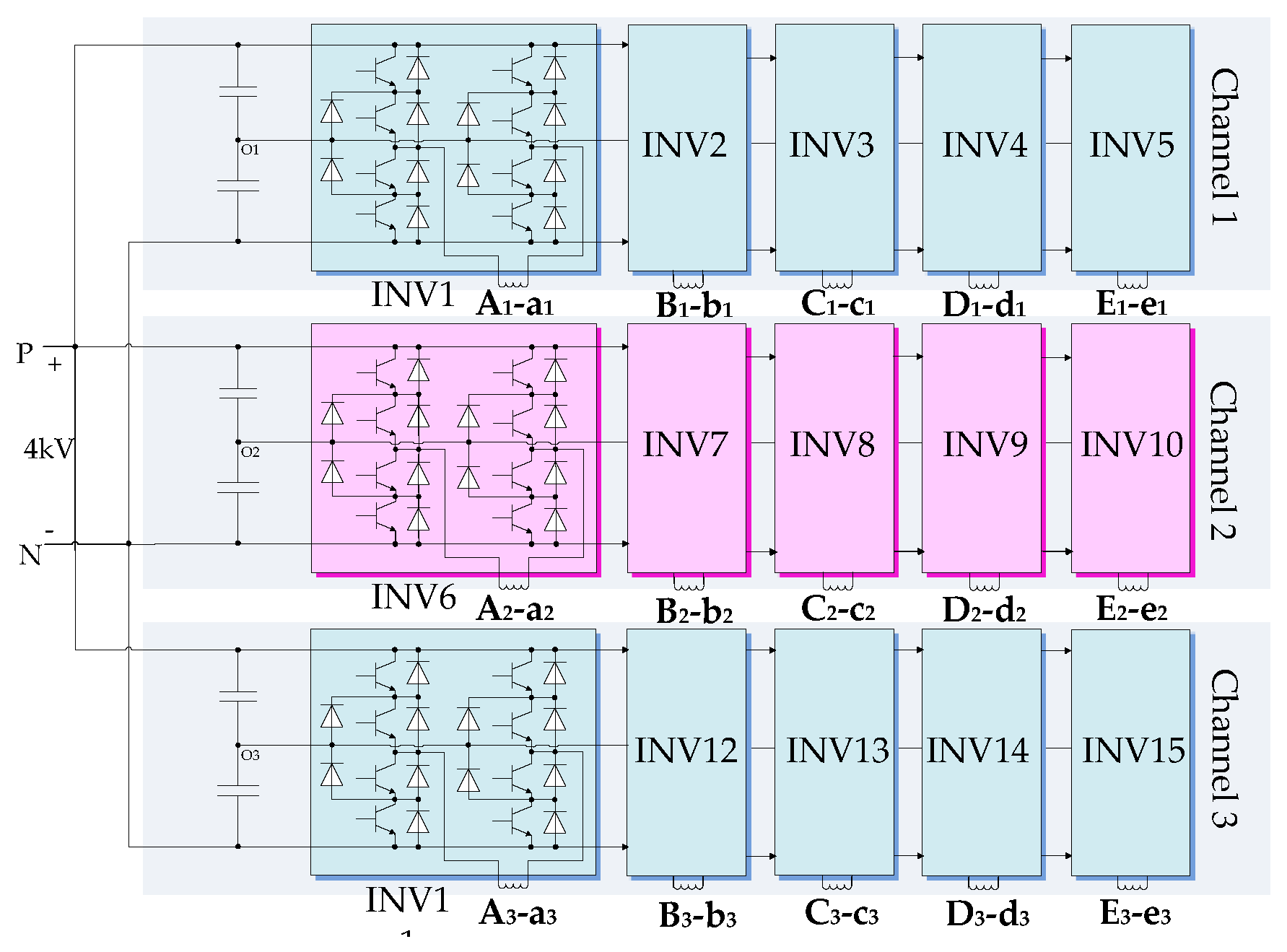
:1. Introduction
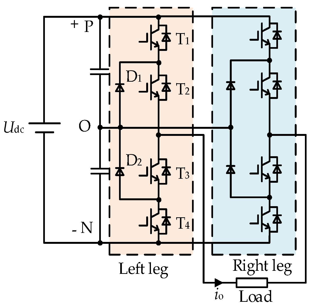
2. Modulation Strategy of Three-Level H-Bridge Inverter
3. NPC Three-Level Inverter PD-PWM Modulation Principle
4. Harmonic Analysis of Output Voltage of NPC Three-Level H-Bridge Inverter
4.1. Harmonic Analysis of Output Voltage without Dead-Time
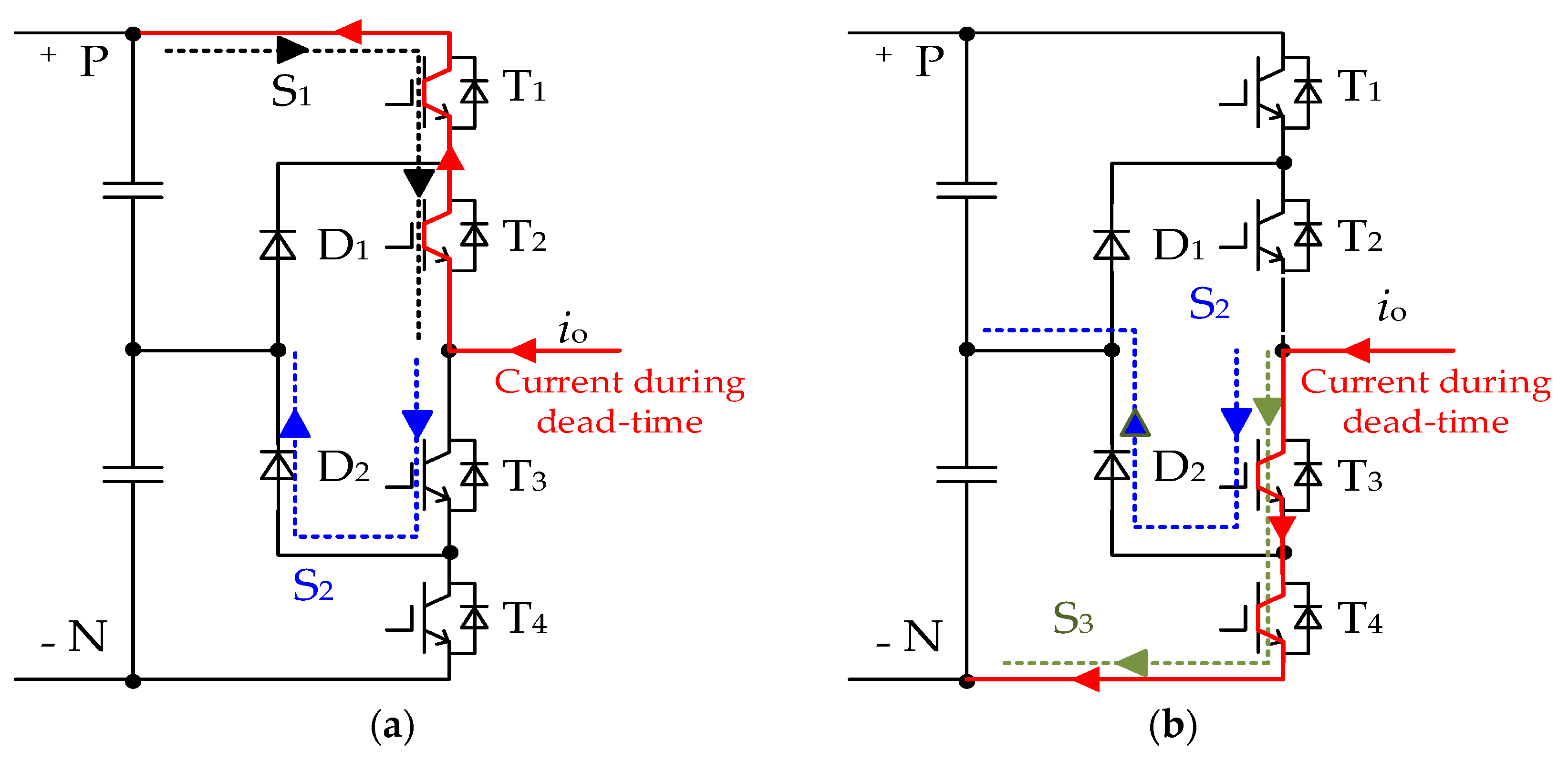
4.2. Harmonic Analysis of Output Voltage with Dead-Time
5. Simulation and Experimental Results
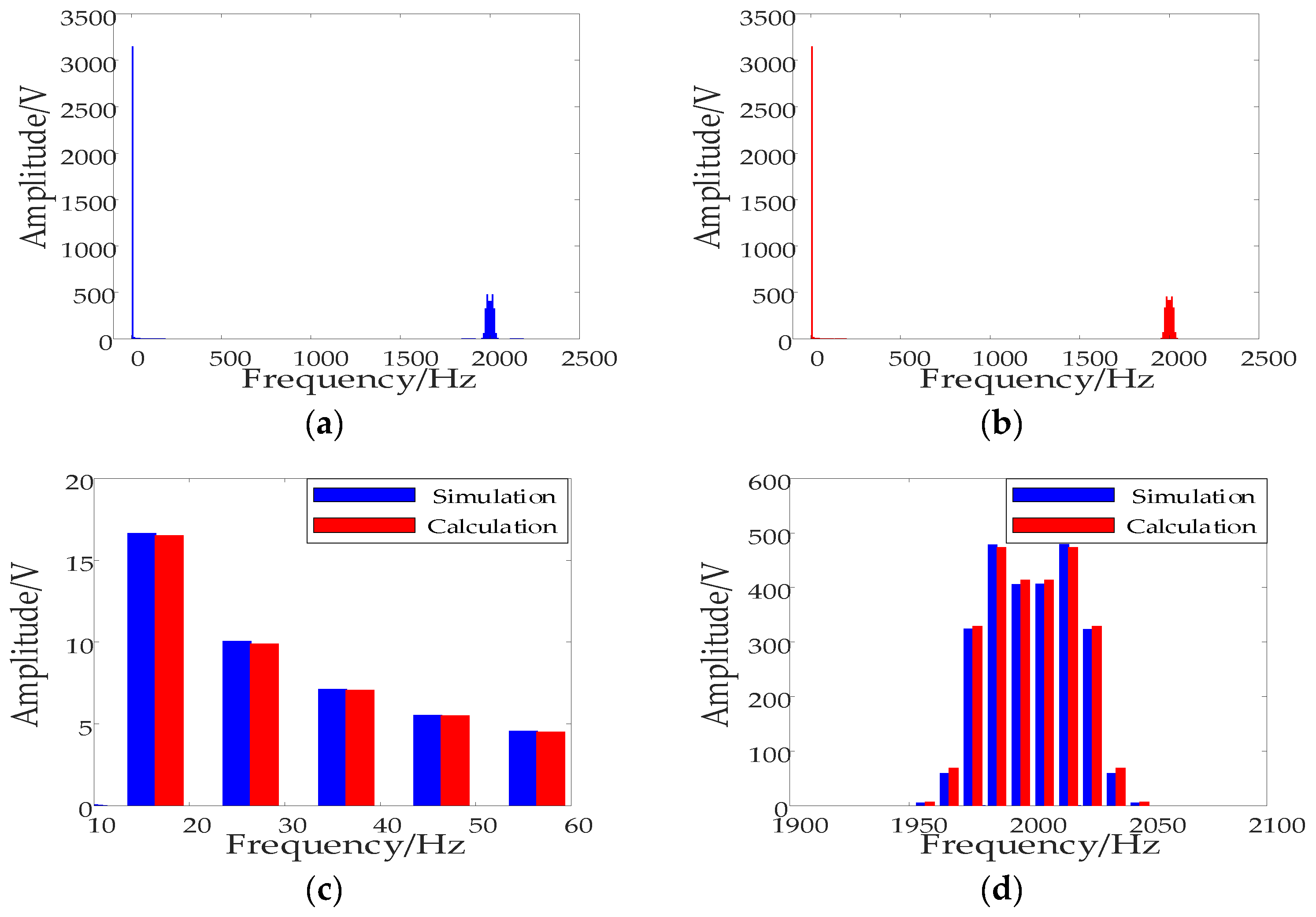
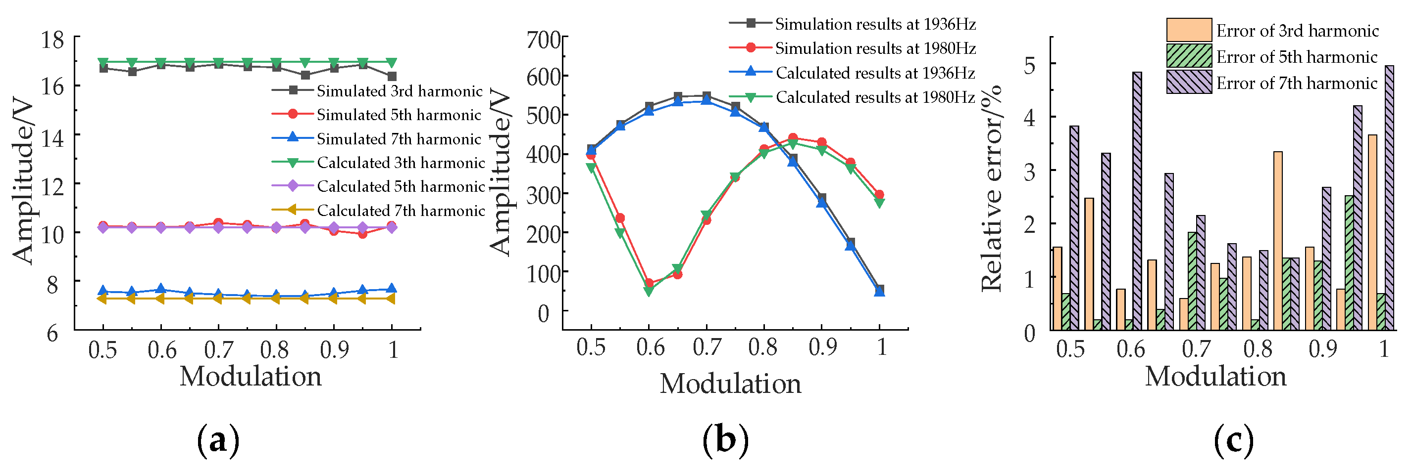
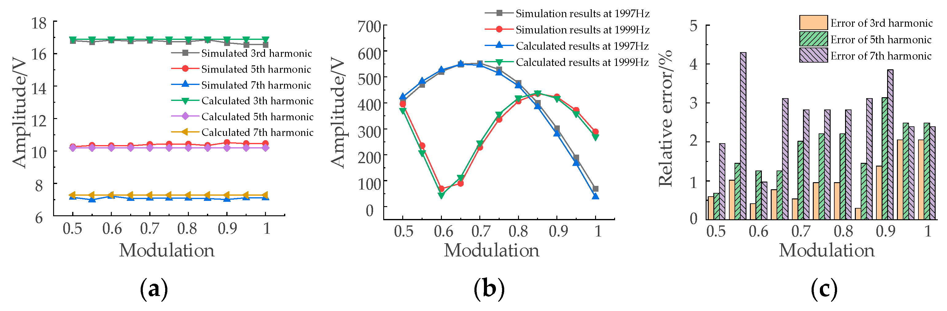
5.1. Simulation Results
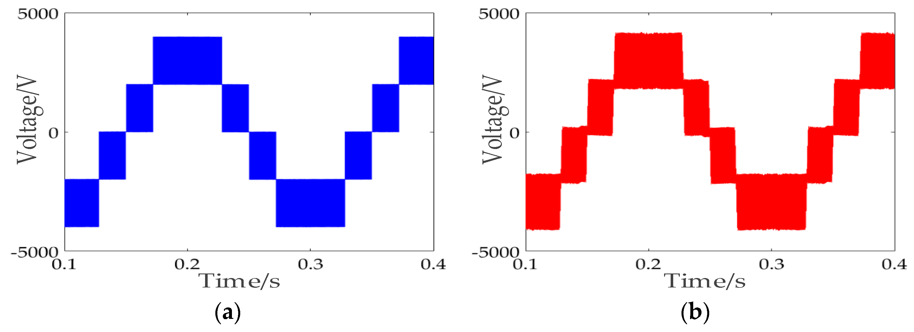
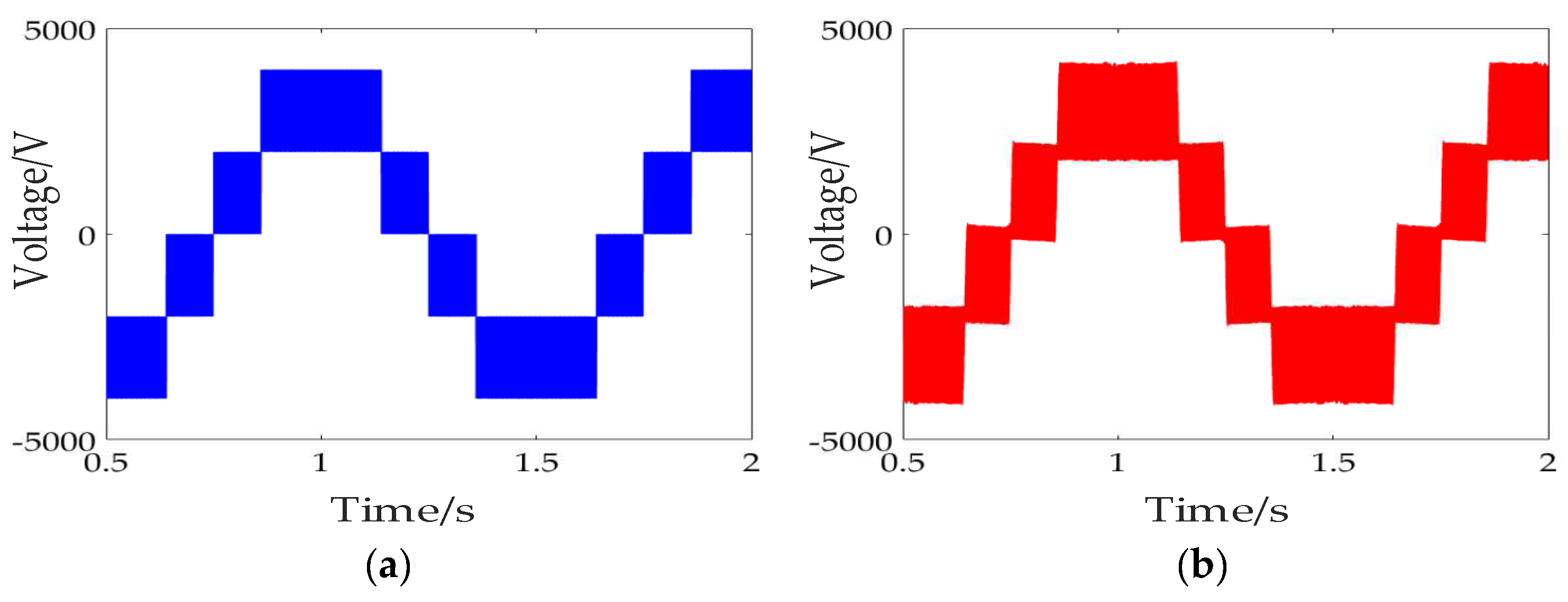
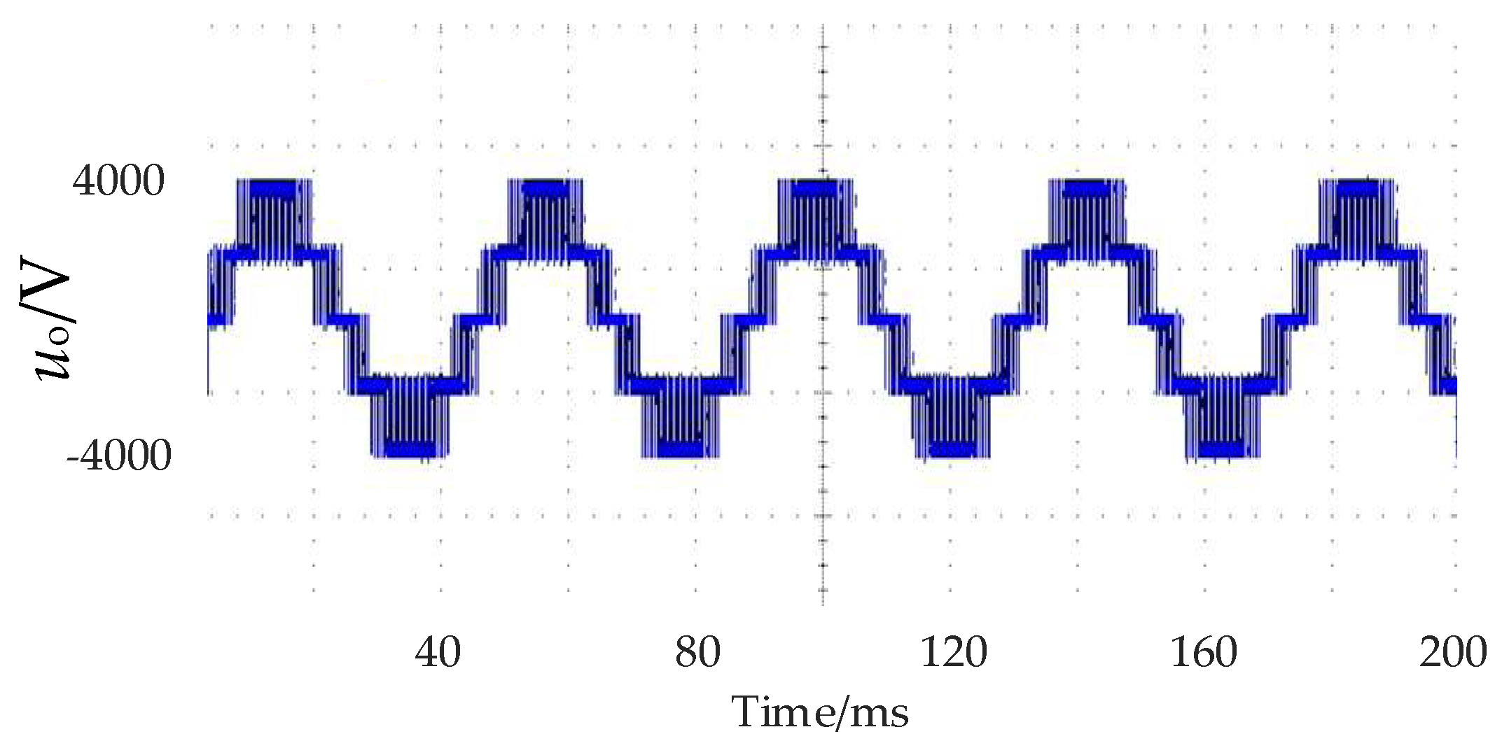
5.2. Experimental Results
6. Conclusions
Author Contributions
Funding
Institutional Review Board Statement
Informed Consent Statement
Data Availability Statement
Conflicts of Interest
Appendix A
Appendix B
References
- Ma, W. On comprehensive development of electrization and informationization in naval ships. J. Nav. Archit. Mar. Eng. 2010, 22, 1–4. [Google Scholar]
- Ma, W. A survey of the second-generation vessel integrated power system. In Proceedings of the IEEE International Conference on Advanced Power System Automation and Protection, Beijing, China, 16–20 October 2011. [Google Scholar]
- Ma, W. Development of vessel integrated power system. In Proceedings of the IEEE International Conference on Electrical Machines and Systems, Beijing, China, 20–23 August 2011. [Google Scholar]
- Dong, Z.; Wang, C.; Cui, K.; Cheng, Q.; Wang, J. Neutral-point voltage-balancing strategies of NPC-inverter fed dual three-phase AC motors. IEEE Trans. Power Electron. 2020, 36, 3181–3191. [Google Scholar] [CrossRef]
- Mukherjee, S.; Giri, S.K.; Banerjee, S. A flexible discontinuous modulation scheme with hybrid capacitor voltage balancing strategy for three-level NPC traction inverter. IEEE Trans. Power Electron. 2018, 66, 3333–3343. [Google Scholar] [CrossRef]
- Choudhury, A.; Pillay, P.; Williamson, S.S. Comparative analysis between two-level and three-level DC/AC electric vehicle traction inverters using a novel DC-link voltage balancing algorithm. IEEE J. Emerg. Sel. Top. Power Electron. 2014, 2, 529–540. [Google Scholar] [CrossRef]
- Wang, S.; Song, W.; Ma, J.; Zhao, J.; Feng, X. Study on comprehensive analysis and compensation for the line current distortion in single-phase three-level NPC converters. IEEE Trans. Power Electron. 2017, 65, 2199–2211. [Google Scholar] [CrossRef]
- Choi, U.M.; Lee, H.H.; Lee, K.B. Simple neutral-point voltage control for three-level inverters using a discontinuous pulse width modulation. IEEE Trans. Energy Convers. 2013, 28, 434–443. [Google Scholar] [CrossRef]
- Donoso, F.; Mora, A.; Cardenas, R.; Angulo, A.; Saez, D.; Rivera, M. Finite-set model-predictive control strategies for a 3L-NPC inverter operating with fixed switching frequency. IEEE Trans. Power Electron. 2017, 65, 3954–3965. [Google Scholar] [CrossRef]
- Sun, C.; Ai, S.; Hu, L. The development of a 20MW PWM driver for advanced fifteen-phase propulsion induction motors. J. Power Electron. 2015, 15, 146–159. [Google Scholar] [CrossRef]
- Nian, H.; Zhou, Y.; Li, J. Control strategy of permanent magnet wind generator based on open winding configuration. Electr. Mach. Control 2013, 17, 80–85. [Google Scholar]
- Reddy, B.V.; Somasekhar, V.T.; Kalyan, Y. Decoupled space-vector PWM strategies for a four-level asymmetrical open-end winding induction motor drive with waveform symmetries. IEEE Trans. Power Electron. 2011, 58, 5130–5141. [Google Scholar]
- Wang, D.; Wu, X.; Guo, Y. Determination of harmonic voltages for fifteen-phase induction motors with non-sinusoidal supply. Proc. Chin. Soc. Electr. Eng. 2012, 32, 126–133. [Google Scholar]
- Hu, L.; Xiao, F.; Lou, X. Research on output voltage abnormal voltage pulses of three-level H-bridge inverter base on cascaded carrier modulation. Proc. Chin. Soc. Electr. Eng. 2019, 039, 266–276. [Google Scholar]
- Thamer, A.H.; Anayi, F.; Packianather, M. Modelling and Control Development of a Cascaded NPC-Based MVDC Converter for Harmonic Analysis Studies in Power Distribution Networks. Energies 2022, 15, 4867. [Google Scholar] [CrossRef]
- Wei, J.; Xue, J.; Zhou, B. Dead-time effect analysis and suppression for open-winding PMSM system with the four-leg converter odulation. Trans. China Electrotech. Soc. 2018, 33, 4078–4090. [Google Scholar]
- Wang, D.; Zhang, P.; Jin, Y. Influences on output distortion in voltage source invertercaused by power devices’ parasitic capacitance. IEEE Trans. Power Electron. 2017, 33, 4261–4273. [Google Scholar] [CrossRef]
- Wei, H.; Wei, H.; Zhang, Y. The controlling performance analysis of the PMSM taking into consideration of the rotor flux harmonics. Trans. China Electrotech. Soc. 2018, 33, 900–909. [Google Scholar]
- Jiang, D.; Shen, Z.; Liu, Z. Progress in active mitigation technologies of power electronics noise for electrical propulsion system. Proc. Chin. Soc. Electr. Eng. 2020, 40, 5291–5302. [Google Scholar]
- Huang, L.; Wang, Z. Development of motor noise theory and noise control technique. Trans. China Electrotech. Soc. 2005, 15, 34–38. [Google Scholar]
- Zhang, R.; Wang, X.; Qiao, D. Influence of pole-arc coefficient on exciting force waves of permanent magnet brushless DC motors. Proc. Chin. Soc. Electr. Eng. 2010, 30, 79–85. [Google Scholar]
- Zhong, Q.; Huang, K.; Wang, G. Harmonic analysis and elimination strategy for voltage source converter under unbalanced three-phase voltage. Autom. Electr. Power Syst. 2014, 38, 79–85. [Google Scholar]
- Wang, F.; Dai, Z.; Wang, J. A variable-angle phase-shifted PWM strategy for cascaded H-Bridge photovoltaic grid-connected inverter. Acta Energ. Sol. Sin. 2020, 41, 144–150. [Google Scholar]
- Jie, Y.; Huang, S.; Liu, L. Accurate harmonic calculation for digital SPWM of VSI with dead-time effect. IEEE Trans. Power Electron. 2020, 36, 7892–7902. [Google Scholar]
- Wu, C.M.; Lau, W.H.; Chung, S.H. Analytical technique for calculating the output harmonics of an H-bridge inverter with dead time. IEEE Trans. Circuits Syst. I Fundam. Theory Appl. 2002, 46, 617–627. [Google Scholar] [CrossRef]
- Dolguntseva, I.; Krishna, R.; Soman, D.E. Contour-based dead-time harmonic analysis in a three-level neutral-point-clamped inverter. IEEE Trans. Power Electron. 2014, 62, 203–210. [Google Scholar] [CrossRef]
- Ji, Z.; Cheng, S.; Wang, D. Current harmonics of PMSMs fed by three-level NPC H-bridge inverters: Characteristics analysis and influence on machine internal magnetic fields. In Proceedings of the International Conference on Electrical Machines and Systems (ICEMS), Harbin, China, 11–14 August 2019. [Google Scholar]
- Hu, L.; Xiao, F.; Xin, Z. Current Suppression Method of Support Capacitor for Three-Level Multiphase H-Bridge Inverter. Proc. Chin. Soc. Electr. Eng. 2020. Available online: https://kns.cnki.net/kcms/detail/11.2107.tm.20220512.1102.001.html (accessed on 13 May 2022).


| Switch Tube | Output Voltage | Switch Mode | |||
|---|---|---|---|---|---|
| T1 | T2 | T3 | T4 | ||
| 1 | 1 | 0 | 0 | +Udc/2 | S1 |
| 0 | 1 | 1 | 0 | 0 | S2 |
| 0 | 0 | 1 | 1 | −Udc/2 | S3 |
| Output Voltage | Range of x | |
|---|---|---|
| −π ≤ x < 0 | 0 ≤ x < π | |
| +Udc/2 | −x/π < Mcosy | x/π < Mcosy |
| 0 | −x/π − 1 ≤ Mcosy < −x/π | x/π − 1 ≤ Mcosy < x/π |
| −Udc/2 | Mcosy < −x/π − 1 | Mcosy < x/π − 1 |
| Description | Value |
|---|---|
| DC bus voltage | 4 kV |
| Carrier frequency | 1000 Hz |
| Load resistance | 0.78 Ω |
| Load inductance | 4.77 mH |
Publisher’s Note: MDPI stays neutral with regard to jurisdictional claims in published maps and institutional affiliations. |
© 2022 by the authors. Licensee MDPI, Basel, Switzerland. This article is an open access article distributed under the terms and conditions of the Creative Commons Attribution (CC BY) license (https://creativecommons.org/licenses/by/4.0/).
Share and Cite
Wu, W.-J.; Hu, L.-D.; Xin, Z.-Y.; Guo, C. Modeling and Analysis of Voltage Harmonic for Three-Level Neutral-Point-Clamped H-Bridge Inverter Considering Dead-Time. Energies 2022, 15, 5937. https://doi.org/10.3390/en15165937
Wu W-J, Hu L-D, Xin Z-Y, Guo C. Modeling and Analysis of Voltage Harmonic for Three-Level Neutral-Point-Clamped H-Bridge Inverter Considering Dead-Time. Energies. 2022; 15(16):5937. https://doi.org/10.3390/en15165937
Chicago/Turabian StyleWu, Wen-Jie, Liang-Deng Hu, Zi-Yue Xin, and Cheng Guo. 2022. "Modeling and Analysis of Voltage Harmonic for Three-Level Neutral-Point-Clamped H-Bridge Inverter Considering Dead-Time" Energies 15, no. 16: 5937. https://doi.org/10.3390/en15165937
APA StyleWu, W.-J., Hu, L.-D., Xin, Z.-Y., & Guo, C. (2022). Modeling and Analysis of Voltage Harmonic for Three-Level Neutral-Point-Clamped H-Bridge Inverter Considering Dead-Time. Energies, 15(16), 5937. https://doi.org/10.3390/en15165937