Abstract
A magnetically insulated transmission line (MITL) is an inevitable choice for ultra-high power density energy transmissions. Its working process is complex, with an obvious influence on the working process of electron beam diodes and other load devices. The power coupling process of an electron beam diode driven by an MITL is a difficult problem in pulse power applications. No research is available on the electron beam characteristics of its anode. In this paper, a fast time response full absorption Faraday cup was developed. An intense electron beam measurement waveform showing the multi-stage characteristics was obtained through measurements using the Faraday cup absorber as the anode of the electron beam diode. The stage characteristics of the beam were in good agreement with the vacuum transmission, magnetic insulation formation, and multi-stage process of the stable magnetic insulation. The beam intensity corresponded with the conduction current of the cathode. It was obviously smaller than the current of the anode. The results reflected the influence of the different processes of the magnetic insulation on the transmission line on the beam waveforms in the diode area and provided a reference for the power transmission of the power device and the load system design.
1. Introduction
An intense beam diode is an important component of pulse power devices [1,2,3,4,5]. This diode can produce a high-energy electron beam and a high-energy X-ray radiation field in different states such as the relativistic electron beam diode used for producing intense electron beams in FLASH II accelerators [6]; irradiation diodes used to produce large areas of high dose-rate, high-energy γ-rays; and self-magnetic pinch diodes used to produce small focal spot X-ray sources on RITS-6 devices [7,8,9,10]. Among these typical intense beam diodes, the characteristics of the electron beam to the anode are the key factors that determine the performance of the diode. Furthermore, the measurement result is the fundamental basis for diode research and the corresponding experimental result analyses. However, due to the rapid intensity change (ns-level frontier), high intensity (hundreds of kA or MA), and high energy (hundreds of keV and even MeV) of electron beams, as well as the complex electromagnetic field, the measurement of intense electron beams has always been a difficult point in the research of all types of electron beam diode devices.
In addition, to significantly improve the energy, dose-rate, and other radiation field indicators, the amplitude of the electronic pulse of a pulse power device reaches several MV or even dozens of MV [11,12,13]. Under an ultra-high voltage, a magnetically insulated transmission line (MITL) is an inevitable choice to achieve the safe and efficient transmission of electric pulses [14,15,16]. The vacuum insulation failure and magnetic insulation establishment in its working process have an obvious effect on the electric pulse waveform, which may further lead to significant changes in the electron beam waveform in the loading area of the electron beam diode. In the stable magnetic insulation stage, the cathode current on an MITL is divided into a conduction current and an electronic charge flow, which also causes great differences in the electron beam intensity and the anode current on the MITL at the front end of the load.
Due to the difficulties in the diagnosis of intense electron beams in the load area and the complex working mechanism of MITLs, ordinary ceramic resistance is unable to obtain a stable signal of resistance at the m Ω level when measuring high-current electron beams at the 100 kA level; in our work, this was solved by introducing a constantan film as the signal resistance. A large-size absorber of a Faraday cylinder, which deals with the wide distribution of the electron beams, can lead to large inductance and capacitance, which increases the response time. In this work, a Faraday cylinder that achieved a fast response at the ns level for the measurement of a high-current relativistic electron beam was developed. It used a constantan thin film as the signal resistance and reduced the inductance of the reflux structure. The waveform characteristics of an electron beam in the power coupling process of an MITL and a high-current electron beam diode are revealed for the first time, providing direct guidance for the construction of large pulse power facilities.
2. Experimental Setup
2.1. Fast Time Response Full Absorption Faraday Cup Design
The equivalent circuit of a full absorption Faraday cup is presented in Figure 1 [17]. The Faraday cup used was equivalent to the current source . The structural inductance between the absorber and the resistor was , and the capacitance was . The structural inductance between the signal resistance and the grounding electrode was , and the capacitance was . and were the equivalent inductance and capacitance on the signal output cable, respectively. The matching situation was . When measuring the intense beam, the signal resistance was much smaller than the impedance of the transmission line (). Thus, was much smaller than and , and it could be approximately assumed that .
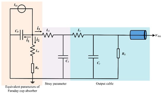
Figure 1.
Equivalent circuit of full absorption Faraday cup.
According to the equivalent circuit of the Faraday cup mentioned above, we assumed that the signal to be measured was a pulse square wave signal. The initial value conditions of and were:
where was the amplitude of the square wave. and met the calculus equation:
The above initial value conditions and the calculus equation suggested that:
From the above current form, the output voltage signal could be described as:
where and .
The output voltage formula showed that the oscillating signal of the exponential attenuation caused by the inductance and capacitance of the Faraday cup could not be ignored. In addition, a significant anomalous skin effect on the fast signal was formed in the Faraday cup as the incident electron beam was the fast pulse signal. Assuming that the frequency of the incident wave was , the anomalous skin depth on the Faraday cup was . The frequency of the distortion signal of the Faraday cup was and the anomalous skin depth on the Faraday cup was . When was much smaller than , the distortion signal was not obvious. At this time, was much greater than , which meant that was much smaller than .
Thus, the key to the t Faraday cup design was to strictly control the stray inductance and capacitance signal to avoid a signal distortion [9,10]. In the structure shown in Figure 2, reflows with the same amplitude and opposite direction were formed along the axial direction of the detector between the signal resistance and the grounding copper current. The reflow structure effectively reduced the structural inductance of the detector. The Faraday cup adopted tight fit, press fit, and other mechanical structures, which ensured the compact structure, thus reducing the structural capacitance.
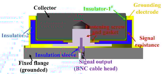
Figure 2.
Structural diagram of the fast time full absorption Faraday cup.
The small signal resistor structure is shown in Figure 3. A 45 μm-thick constantan foil was used to prepare the signal resistor by cutting. The amplitude of the signal resistor was adjusted by controlling the number of parallel lines and the structure on each current path. In addition, it adopted the parallel of 8 spoke wheel membrane resistors and ensured that the resistance values R1 to R8 of the 8 parallel branches were equal. I1–I8 were equivalent in the process of the signal acquisition, which could reduce the structural inductance of the signal resistance.
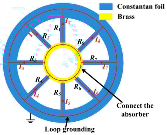
Figure 3.
Diagram of the radiated signal resistance structure.
2.2. Voltage Division Ratio Demarcation of the Full Absorption Faraday Cup
Overall demarcation was adopted to estimate the frequency response, signal distortion, and voltage division ratio because accurately measuring the inductance and capacitance of the Faraday cup was difficult. The measurement circuit was calibrated by a DC high-voltage gap discharge. The calibration circuit is shown in Figure 4.
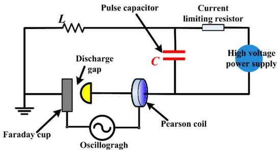
Figure 4.
Calibration circuit of the measurement circuit.
The beam signals of the Faraday cup and the current signals of the Pearson coil obtained from the experiment are shown in Figure 5; these were in good agreement. The pulse front of the discharge waveform was approximately 32 ns, which was similar to the characteristics of the measured waveform. The response of the measurement circuit met the requirements. The measured signals were compared with the signals of the Pearson coil to obtain a sensitivity of 636 A/V. The signal resistance could be deduced to 1.57 mΩ according to the voltage division ratio, which was suitable for the 100 kA intense electron beam measurement.
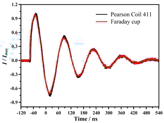
Figure 5.
Calibration waveform of Faraday cup.
3. MITL Experimental Platform Design
The geometric structure of the secondary MITL could be accurately estimated according to the Creedon laminar flow theory. The voltage loaded between the anode and cathode of the MITL was assumed to be , and the corresponding relativistic factor was :
where were the static mass of the electron and the charge amount, respectively. For the known , could be obtained by Equation (2):
where was the relativistic factor that corresponded with the boundary potential in the electron charge layer. When , the gap between the anode and the cathode was filled with electrons. At this time, the trajectory of the electrons just swept over the surface of the anode.
The geometric structure factor of the coaxial cylinder structure was:
where were the outer diameter of the inner conductor and the inner diameter of the outer conductor, respectively. The relationship between the geometric factors and could be solved by the expression of the minimum current when the MITL was running. The expression of the minimum current was:
The relationship between the minimum current and the operating impedance and the cathode–anode voltage met:
The diameter of the outer cylinder of the MITL was set as 234 mm. The regularity among the working voltage , running impedance , and critical current of the MITL is shown in Figure 6. The higher the running impedance of the MITL, the higher the corresponding vacuum impedance and the lower the was in meeting the critical condition of the magnetic insulation; thus, it was easier to realize the magnetic insulation.
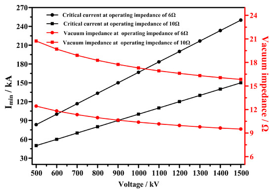
Figure 6.
Variation in the critical current with the working voltage under different running impedances.
For the pulse source part, based on the Jianguang-I accelerator [18], an experimental platform of a coaxial cylindrical MITL was set up. The capacitance of the drive source Marx generator was 0.67 nF, the series resistance of the circuit was approximately 6 Ω, and the highest output voltage was about 3.2 MV. The charging time for the forming line was roughly 300 ns, and the impedance of the water medium-forming line and the transmission line was 7.8 Ω. Based on the MITL characteristics, the radii of the inner and outer cylinders of the coaxial cylindrical MITL were 90 mm and 117 mm, respectively. The load adopted the electron beam diode. The gap of the diode was adjusted to conveniently change the working state of the MITL. In the experiment, the full absorption Faraday cup was installed in the anode area of the electron beam diode and the graphite absorber was used as the diode anode. The experimental platform for the MITL-driving electron beam diode is shown in Figure 7.
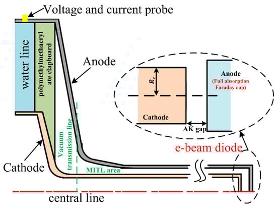
Figure 7.
The experimental platform for MITL-driving electron beam diode.
4. Experimental Results and Characteristic Analysis of The Electron Beam
The regional pulse electrical parameters of the MITL in a typical state are shown in Figure 7. The amplitude of the pulse voltage was 670 kV and that of the pulse current was 137 kA. According to the analytical formula in Section 3, the critical current of the magnetic insulation was 81 kA, which met the magnetic insulation condition. The peak power was always in a good state of magnetic insulation.
Assuming that the electron emission thresholds on the surface of the cathode of the electron beam diode and the cathode of the MITL were both 150 kV/cm, both the anode and cathode of the diode had a flat-plat structure with the load gap set to 6 mm. Furthermore, when the electric field intensity on the surface of the cathode of the diode reached the electron emission threshold, the diode voltage was 90 k V, which corresponded with 17 ns (A time) of the pulse voltage waveform (Figure 8). The radii of the inner and outer cylinders were 90 mm and 117 mm, respectively. According to the formula , when the threshold stress of the electron emission was achieved, the gap voltage between the anode and cathode of the MITL was 354 kV, which corresponded with 35 and 103 ns of the pulse voltage waveform, as shown in Figure 8 (B1 and B2 times).
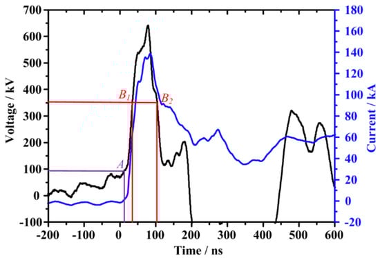
Figure 8.
Working voltage and current of MITL in a typical state.
Corresponding with the pulse electrical parameter state shown in Figure 8, the electron beam waveform on the load of the diode was measured by experiments (Figure 9). The electron beam showed typical multi-stage characteristics.
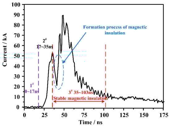
Figure 9.
Electron beam waveform obtained by full absorption Faraday cup.
According to the changing process of the pulse voltage with time, the working process of the MITL–electron beam diode power coupling system was divided into four stages.
Stage one (0~17 ns): The potential difference between the transmission line and the diode was 0–90 kV. In this period, the vacuum transmission line and the cathode of the electron beam diode did not emit electrons. The coaxial transmission line achieved the pulse power transmission in the form of a vacuum transmission line. The gap between the anode and cathode of the electron beam diode was equivalent to a flat capacitor structure. The capacitor was charged when the electrical pulse reached the load area. The displacement current was produced in the charging process. The relationship between the displacement current and the charging voltage met Formula (10):
where was the pulse voltage frequency. The electrical pulse front in Figure 8 was ~80 ns; after the calculation, . was the permittivity of the vacuum, and and were the electrode area and the gap of the diode, respectively. After the calculation, when the voltage was 90 kV, the corresponding displacement current . As the signal resistance was only ~1.57 mΩ, the bias voltage produced by the displacement current on the signal resistance was very small. Figure 8 shows that there was no obvious signal output in the stage of 0–17 ns.
Stage two (17–35 ns): The potential difference between the transmission line and the diode gap was 90–354 kV. In this period, the coaxial transmission line still realized a pulse power transmission in the form of a vacuum transmission line. The cathode of the electron beam diode began to emit electrons. The power coupling system was equivalent to the electron beam diode driven by the vacuum transmission line. After crossing over the gap between the anode and the cathode, the electron beams emitted by the cathode of the electron beam diode bombarded the Faraday cup as the anode of the diode. The electron beam intensity was positively correlated with the working voltage of the diode, which met the Child–Langmuir formula:
The coaxial cylinder area achieved a maximum voltage of 354 kV during the electric pulse power transmission in the form of a vacuum transmission line, which corresponded with the electron beam . In the stage of 17 to 35 ns in the experimental results shown in Figure 8, the beam intensity significantly increased with the voltage. At 35 ns, the electron beam intensity was 51 kA, which was in good agreement with the theoretical model of the electron beam diode.
Stage three (35–103 ns): The potential difference between the transmission line and the diode gap was greater than 354 kV. In this period, the coaxial cylinder area was transformed from the vacuum transmission to the magnetic insulation. In the process of the state of transformation, the cathode of the transmission line emitted electrons, thereby leading to the failure of the vacuum insulation, resulting in a power transmission cut-off in a short period. The size of the diode cathode was much smaller than the radius of the cathode of the coaxial cylindrical MITL, thereby avoiding the entry of the electric charge in the stable magnetic insulation stage into the diode gap. The conduction current of the cathode on the MITL entered the load area and changed into the electron beams. They were then collected by the full absorption Faraday cup. The electron beam reflected the conduction current of the cathode of the MITL.
In the laminar flow theory, the conduction current of the cathode and the current of the anode met the following formula:
At the time of the peak pulse, and the conduction current of the cathode was , which corresponded with the electron beam intensity of the diode gap in the laminar flow theory. In the experimental results shown in Figure 9, the peak beam was 89 kA, which was slightly lower than the theoretical value.
Notably, the electron beams sharply reduced during the period later than the formation of magnetic insulation at 35 ns. The analysis indicated that it may have been related to the vacuum insulation failure and the magnetic insulation establishment on the transmission line. The simulation results in the early stage generally suggested that this process, being a sub-nanosecond process, was very rapid when being reflected in the electric pulse waveform. From the beam waveform obtained through the measurement, the duration of the beam intensity from the sharp reduction to recovering to the theoretical value reached 7 ns. The analysis showed that this phenomenon was because the wave reflection in the power coupling process in the power coupling system of the electron beam diode driven by the MITL could cause the amplification of the waveform distortion in the beam waveform. The physical mechanism of this phenomenon needs to be studied further.
Stage four (~103 ns): At 103 ns, the coaxial transmission line transformed from the magnetic insulation into the vacuum transmission line state. The transformation of the transmission state could lead to changes in the beam waveform and intensity. However, this process resulted in the vaporization of graphite on the surface of the collector as well as plasma formation, ion diffusion, and other processes because of the strong electron beam that bombarded the graphite collector during the experiment, which accumulated high energy in a short time. These processes affected the working process of the Faraday cup and the accuracy of the beam measurement. At the back of the beam waveform, as shown in Figure 9, the high-frequency interference became significant, which may have been related to the surface state change and evolution of the absorber. In this case, the beam measurement experienced a significant deviation.
5. Conclusions
Diagnostic research on an intense electron beam was conducted for the first time in view of an electron beam diode driven by an MITL. A full absorption Faraday cup with low inductance and a fast time response was developed. The voltage division ratio of the full absorption Faraday cup was 636 A/V and the signal resistance was 1.57 mΩ. With the full absorption Faraday cup absorber as the anode of the electron beam diode, a pulse waveform of the electron beam was obtained through experiments. The beam waveform showed typical multi-stage characteristics with the working process of the front-end MITL. These stages were in good agreement with the formation time and conduction current of the magnetic insulation through theoretical calculations. The experimental results revealed the characteristics of the electron beams in the loading area of the complex power coupling system of the electron beam diode driven by the MITL for the first time. Furthermore, the designed full absorption Faraday cup met the beam measurement requirements in a complex electromagnetic environment, providing a reference for subsequent research on intense electron beam diodes.
Author Contributions
Conceptualization, P.Z. and H.Y.; methodology, D.L.; validation, P.Z. and J.S.; formal analysis, P.Z. and W.L.; data curation, P.Z. and W.L.; writing—original draft preparation, P.Z. and W.L. All authors have read and agreed to the published version of the manuscript.
Funding
This work was supported by the National Natural Science Foundation of China (Grant Nos. 11875224 and 12027811) and the State Key Laboratory of Intense Pulsed Radiation Simulation and Effect (Grant No. SKLIPR.1904).
Informed Consent Statement
Not applicable.
Data Availability Statement
Data presented in this study are available on request from the first author.
Conflicts of Interest
The authors declare no conflict of interest.
References
- Qiu, A.C. Application of Pulse Power Technology; Shaanxi Science and Technology Press: Xi’an, China, 2016. [Google Scholar]
- Zeng, Z.Z. Introduction to Practical Pulsed Power Technology; Shaanxi Science and Technology Press: Xi’an, China, 2003. [Google Scholar]
- Pai, S.T.; Zhang, Q. Introduction to High Power Pulse Technology; World Scientific: Singapore, 1995. [Google Scholar]
- Bluhm, H. Pulsed Power Systems; Springer: Karlsruhe, Germany, 2006. [Google Scholar]
- Mesyats, G.A. Pulsed Power; Kluwer Academic/Plenum Publishers: New York, NY, USA, 2005. [Google Scholar]
- Yang, H.L.; Qiu, A.C.; Sun, J.F.; He, X.P.; Tang, J.P.; Wang, H.Y.; Li, H.Y.; Li, J.Y.; Ren, S.Q. Preliminary research results for the generation and diagnostics of high power ion beams on flash ii accelerator. Acta Phys. Sin. 2004, 53, 406–412. [Google Scholar] [CrossRef]
- Michael, G.M.; Nichelle, B.; Michael, E.C.; Sean, D.F.; Mark, D.J.; Mark, L.K.; Joshua, J.L.; Dan, S.N.; Bryan, V.O.; Matthew, E.S.; et al. Contribution of the backstreaming ions to the self-magnetic pinch (SMP) diode current. Phys. Plasmas 2018, 25, 043508. [Google Scholar]
- Renk, T.J.; Oliver, B.V.; Kiefer, M.L.; Webb, T.J.; Leckbee, J.J.; Johnston, M.D.; Simpson, S.; Mazarakis, M.G. Characterization of self-magnetic pinch (SMP) radiographic diode performance on RITS-6 at Sandia National Laboratories. I. Diode dynamics, DC heating to extend radiation pulse. Phys. Plasmas 2022, 29, 023105. [Google Scholar] [CrossRef]
- Patel, S.G.; Johnston, M.D.; Webb, T.J.; Bennett, N.L.; Welch, D.R.; Gilgenbach, R.M.; Cuneo, M.E.; Kiefer, M.L.; Leck-bee, J.J.; Mazarakis, M.G.; et al. Zeeman spec-troscopy as a method for determining the magnetic field distribution in self-magnetic-pinch diodes. Rev. Sci. Instrum. 2018, 89, 10123. [Google Scholar] [CrossRef] [PubMed]
- Renk, T.J.; Oliver, B.V.; Kiefer, M.L.; Webb, T.J.; Leckbee, J.J.; Johnston, M.D.; Simpson, S.; Mazarakis, M.G. Characterization of self-magnetic pinch radiographic diode performance on RITS-6 at Sandia National Laboratories. II. Coupling between the inductive voltage adder and the SMP load. Phys. Plasmas 2022, 29, 023106. [Google Scholar] [CrossRef]
- Luo, W.; Zhang, J.; Li, Y.; Wang, H.; Liu, C.; Zhang, P.; Guo, F. Investigation on current loss of high-power vacuum transmission lines with coaxial-disk transitions by particle-in-cell simulations. Plasma Sci. Technol. 2021, 23, 115601. [Google Scholar] [CrossRef]
- Zhang, P.F.; Hu, Y.; Yang, H.L.; Sun, J.; Wang, L.P.; Cong, P.T.; Qiu, A.C. Experimental study on magnetically insulated transmission line electrode surface evolution process under MA/cm current density. Phys. Plasmas 2016, 23, 033105. [Google Scholar] [CrossRef]
- Zhang, P.F.; Sun, J.F.; Sun, F.J.; Qiu, A.C.; Sun, J.; Hu, Y.; Cong, P.T. Simulation Analysis of a Pulsed Compact FLTD System for Large-Area Hard X-Ray Sources. IEEE Trans. Plasma Sci. 2016, 44, 803–807. [Google Scholar] [CrossRef]
- Luo, W.; Zhang, J.; Li, Y.; Wang, H.; Liu, C.; Guo, F.; Zou, W. Particle-in-cell simulations of cathode plasma evolution in small-gap magnetically insulated transmission lines. J. Appl. Phys. 2019, 126, 243305–243314. [Google Scholar] [CrossRef]
- Zhang, P.F.; Yang, H.L.; Sun, J.; Hu, Y.; Lai, D.G.; Li, Y.D.; Wang, H.G.; Cong, P.T.; Qiu, A.C. Experimental study on the current transmission efficiency for the transition structure of “vacuum transmission line MITL” on Flash-II accelerator. IEEE Trans. Plasma Sci. 2016, 44, 1902–1906. [Google Scholar] [CrossRef]
- Zhang, P.F.; Qiu, A.C.; Li, Y.D.; Wang, H.G.; Sun, J.; Hu, Y.; Sun, F.J.; Cong, P.T. Design and simulation study of MITL for Multi-stage FLTD in Series. IEEE Trans. Plasma Sci. 2016, 44, 1928–1932. [Google Scholar] [CrossRef]
- Samuel, A.L.; Robert, E.; Chris, F.; Jessica, I.; Wang, T.Y.; Shao, L.; Allen, N.; Gates, D.; Neilson, H. Development of a Faraday cup fast ion loss detector for keV beam ions. Rev. Sci. Instrum. 2019, 90, 093504. [Google Scholar]
- Sun, F.J.; Qiu, A.C.; Yang, H.L.; Zeng, J.T.; Gai, T.Y.; Liang, T.X.; Yin, J.H.; Sun, J.F.; Cong, P.T.; Huang, J.J.; et al. Pulsed X-ray source based on inductive voltage adder and rod pinch diode for radiography. High Power Laser Part. Beams 2010, 22, 936–940. (In Chinese) [Google Scholar]


Disclaimer/Publisher’s Note: The statements, opinions and data contained in all publications are solely those of the individual author(s) and contributor(s) and not of MDPI and/or the editor(s). MDPI and/or the editor(s) disclaim responsibility for any injury to people or property resulting from any ideas, methods, instructions or products referred to in the content. |
© 2023 by the authors. Licensee MDPI, Basel, Switzerland. This article is an open access article distributed under the terms and conditions of the Creative Commons Attribution (CC BY) license (https://creativecommons.org/licenses/by/4.0/).