Article

Method and Equipment for Reducing the Efficiency Degradation of Monocrystalline Passivated Emitter and Rear Cells

1
Jiangsu Key Laboratory of Materials and Technology for Energy Conversion, College of Materials Science & Technology, Nanjing University of Aeronautics & Astronautics, Nanjing 210016, China
2
Ycergy (Suzhou) Technology Co., Ltd., Suzhou 215121, China
3
Jiangxi HAC General Semitech Co., Ltd., Jiujiang 332001, China
*
Author to whom correspondence should be addressed.
Energies 2024, 17(7), 1550; https://doi.org/10.3390/en17071550
Submission received: 2 February 2024 / Revised: 1 March 2024 / Accepted: 21 March 2024 / Published: 23 March 2024
(This article belongs to the Section A2: Solar Energy and Photovoltaic Systems)

Abstract

:
Infrared soldering as a step in module encapsulation, which would cause light-induced degradation (LID) and light- and elevated-temperature-induced degradation (LeTID) effects on solar cells, may cause efficiency mixing among solar cells that were originally in the same grade within the module after soldering. Furthermore, the problem of bright and dark regions would appear, which would result in a decrease in the CTM value. Current injection is considered to be one of the effective methods to solve the above problem. However, after the current injection treatment, there is still a 10% probability of the appearance of bright and dark regions in modules. In this work, we first adopted the conventional current injection process in monocrystalline passivated emitter and rear cells (PERCs). The effects of injected currents, temperature and time were systematically optimized, and cells with or without the current injection under the optimal parameters were illuminated with 1 sun at 85 °C for 25 h. Secondly, a piece of equipment was developed to further stabilize the performance of solar cells and improve the CTM value. The results showed that the best current injection parameters were a temperature of 185 °C, an injected current of 11 A and an injection time of 770 s. Compared with the cells without any pretreatment, the relative changes in the η, Voc, Isc and FF of the cells pretreated with the optimal conditions mentioned above were 0.23%, 0.08%, 0.02% and 0.08% larger, respectively, after 25 h of degradation. Then, solar cells processed by current injection were processed with our equipment, and the probability of a problem occurring was reduced from 10% to 2%. Meanwhile, the CTM value increased by 0.4%. Finally, a balance mechanism between H0 and H0-X has been proposed to explain the mechanism of the equipment.

1. Introduction

In 1973, Fischer et al. first observed the power decay caused by illumination in boron-doped silicon cells, called light-induced degradation (LID) [1]. The research on LID has been relatively sufficient, and the root cause of this has been recognized to mainly be B-O defects [2]. In 2012, Ramspeck et al. studied a novel degradation mechanism in polycrystalline silicon solar cells, and this degradation was named light- and elevated-temperature-induced degradation (LeTID) by Kersten et al. in 2015 [3,4]. Unlike LID, LeTID would reach saturation degradation at high temperatures for a longer period [5,6]. The LeTID phenomenon has been found in all types of crystalline silicon materials, including n-type and p-type silicon, with different degrees of degradation [7,8,9,10]. In the past, LeTID was reported to cause a 16% reduction in relative efficiency [11].
In addition, power loss also inevitably occurs during the process of encapsulating solar photovoltaic modules [12,13,14]. The factors contributing to the loss could be divided into three broad categories: optic, geometric and electric factors. To quantify this loss, the cell-to-module (CTM) power ratio was defined, which could be calculated by the ratio of module power and the individual cells’ power. Philipps et al. encapsulated monocrystalline 156 × 156 mm2 solar cells into a 60-cell module and found its CTM value was 87% [15]. In 2016, Hanifi et al. showed that some of the top solar cell conversion efficiencies in the market were 21.25 ± 0.4%, with corresponding photovoltaic module efficiencies of 19.2 ± 0.4%. This corresponds to a CTM ratio of 90% [16]. Subsequently, in 2022, Ballif et al. showed that the CTM value is usually around 95~97% [17]. In addition, Hanifi et al. found that the CTM values of full-size cell modules were between 93% and 97%, while those of half-size cell modules made from the same materials were over 100%. Meanwhile, half-size cell modules with a narrower tab width could achieve a higher CTM value of 102% [18]. The reason why half-size cell modules can improve CTM values can be attributed to lower electrical losses and higher optical gains. It is crucial to improve the CTM ratio whether through the processing of solar cells or by changing the module design.
In this article, focusing on the issue of the bright and dark regions caused by LID or LeTID resulting from infrared soldering, we proposed a two-step approach. Firstly, we treated solar cells with current injection, which would not only mitigate the degradation but also be suitable for mass processing. In this section, the current injection parameters were optimized and the changes in electrical performance parameters (open circuit voltage (Voc), short-circuit current (Isc), fill factor (FF) and η) before and after current injection were compared. Secondly, to further reduce the probability of bright and dark regions and continue to increase the CTM value based on the half-size cell module, a piece of equipment was developed. Finally, the mechanism of the equipment that accelerates degradation and regeneration was revealed.

2. Experimental Section

2.1. Preparation of PERC Solar Cell

A batch of boron-doped p-type monocrystalline silicon wafers was used in this experiment. The silicon wafers were sliced by diamond wire cutting technology, with a thickness of 150 ± 20 μm, a size of 182 mm × 182 mm and a resistivity of 0.4~1.1 Ω·cm.
The front side of the silicon wafers was first processed by 10~20% NaOH solutions and then textured with HF/HNO3 solution. All wafers were pyramid textured with approximately 4 μm per side (a weight loss of 0.34 g). After that, the textured wafers were diffused with POCl3, followed by a wet chemical etching process to remove phosphosilicate glass (PSG) and P-N junctions at the edges, resulting in a resistance of 110~130 Ω/sq. Then, the 10.8 nm Al2O3 layer was deposited on the rear side, and the SiNx layer was deposited on both sides of the silicon wafers by PECVD in 2 in 1 MAiA (Meyer Burger, Thun, Switzerland). The thickness of the front- and rear-side SiNx layer was kept at 75 nm and 120 nm, respectively, while the refractive index of the front and side SiNx layer was kept at 2.0 and 2.2, respectively. On the rear side, Al2O3/SiNx rear-side stacked passivation was ablated by a laser (DR, 525 nm) to form local openings. The dot-to-dot distance was 30 μm, and the line-to-line distance was about 17.3 mm. Finally, standard screen printing was used to screen-print silver and aluminum on the front and rear surfaces of the wafers, which formed good ohmic contact through the firing process.
After the above processes were completed, solar cells were placed in the anti-LeTID furnace, which can provide forward current injection in a dark environment. Cells were preheated in the first chamber, the temperature of which reached about 120 °C. Then, the injection current, temperature and time could be adjusted in the following chambers, in which cells were electrified through the upper and lower plates. Finally, they entered the cooling chamber for 40 min.
We set up three experiments to optimize the current injection parameters to achieve the best anti-degradation effect. The cells in Group I were treated with different injected currents (7, 9, 11, 13, 15 A) at 185 °C for 700 s. The cells in Group II were treated with 11 A and 700 s at different temperatures (170, 185, 200, 215, 230 °C), while the cells in Group III were injected at different times (560, 630, 700, 770, 840 s) at 11 A and 185 °C. Then, we took the efficiency gain (EGE), which can be calculated by Equation (1), to characterize the increase in conversion efficiency after current injection and efficiency degradation (EDE), which can be calculated by Equation (2), to reveal the decrease in conversion efficiency after degradation (1 sun, 85 °C, 10 h). The optimal parameters were obtained when the sum of EGE and −EDE was the largest.
EGE= η after current injection − η before current injection
EDE = η after current injection (before degradation) − η after degradation
where η denotes the conversion efficiency [%].
On the other hand, to show the benefit of current injection, we used solar cells without any pretreatment as control cells and the other pretreated cells under optimal current injection conditions to perform experiments. Both of them were illuminated with 1 sun at 85 °C. It should be noted that the evolution of η, Voc, Isc and FF during degradation was presented by the relative change, which could be calculated by Equation (3).
X t = x t x 0 x 0   ×   100 %
where x(0) and x(t) denote the electrical performance parameters, which can be η [%], Voc [V], Isc [A] or FF [%]; 0 denotes before degradation; t denotes each step of degradation (5, 10, 15, 20, 25 h).

2.2. Characterization Methods

The electrical performance of solar cells was measured by a German Halm tester under standard testing conditions (AM1.5G, 1000 W/m2, 25 ± 2 °C). The external quantum efficiency (EQE) of solar cells was investigated using the solar cell measurement system of Bentham PVE300 (Suzhou Vision Intelligence Technology Co., Ltd., Suzhou, China). The electroluminescent (EL) images of solar cells and modules were tested at room temperature by Kopad KP-X-D-N (Suzhou Kepai Automation Equipment Co., Ltd., Suzhou, China).

3. Results and Discussion

3.1. Impact of Current Injection Parameters on the EGE and EDE of Solar Cells

Figure 1a represents the evolution of the EGE and EDE of cells that were injected with different currents (7, 9, 11, 13, 15 A) at 185 °C for 700 s. The pretreatment process of the current was beneficial to increase the η of cells, and the maximum EGE, which was 0.081%, occurred at a current of 13 A. However, the EDE presented a linear increasing tendency when the current was greater than 11 A. Thus, we chose 11 A as the optimal injection current, under which, the sum of EGE and −EDE was the largest.
As depicted in Figure 1b, 11 A current injection for 700 s at different temperatures (170, 185, 200, 215, 230 °C) also induced a change in η. As the temperature increased, the EGE first increased and then decreased. When the temperature was 230 °C, the current injection could even reduce the η of solar cells. In other words, EGE presented a negative value at 230 °C. Under this condition, solar cells were more likely to burn through, especially in areas with abundant crystallographic defects. It is worth noting that the burning-through area reflected in the EL image was a black halo highlighted by a red square in Figure 1d; a similar phenomenon has also been observed by Hu et al. [19]. In addition, the trend presented by EDE generally increased. Overall, the optimum temperature was 185 °C, under which, the EGE and EDE were 0.067% and 0.044%, respectively.
In Figure 1c, the injection current was maintained at 11 A, the temperature was 185 °C and the current injection time was adjusted (560, 630, 700, 770 and 840 s). The largest EGE and the smallest EDE were obtained at the current injection time of 770 s, which were 0.070% and 0.042%, respectively.
It can be noticed that almost all these cells showed an increase in conversion efficiency under different conditions of injection current parameters. A similar phenomenon has been reported in previous research [19,20]. This may be related to the passivation of crystal defects by movable hydrogen atoms introduced by SiNx under electrical injection conditions within this temperature range. Meanwhile, the precipitation of metals is also related to this phenomenon, as Pickett et al. found that reducing the concentration of iron-related point defects can improve the electrical performance of solar cells [21]. In addition, the existing regeneration of an as-fired LeTID defect may exist. The occurrence of this phenomenon may be caused by one of the reasons, or it may be a joint result of the above reasons. In a word, the concentration of excess carrier injection should be appropriate to maximize the LeTID suppression effect. Therefore, the optimal current injection conditions obtained through the experiment were 11 A, 185 °C and 770 s.

3.2. Comparison of Degradation Characteristics with or without Current Injection

Figure 2 shows the relative change in electrical performance parameters when PERCs injected with currents under the optimal preparation conditions mentioned above were exposed to 1 sun illumination at 85 °C compared to the control cells that were not injected with currents. As shown in Figure 2a, the relative change in Voc seemed to be relatively small. After 25 h of degradation, the relative changes in Voc were −0.06% and −0.14% with and without current injection, respectively. Similarly, the relative change was also small. Unlike Voc and Isc, the relative changes in FF appeared to be relatively large, which are presented in Figure 2c. Overall, according to Figure 2d, it is evident that current injection is beneficial to mitigate degradation. After 25 h of degradation with 1 sun illumination at 85 °C, the relative changes in η, Voc, Isc and FF of the cells pretreated with the optimal conditions mentioned above were −0.54%, −0.06%, −0.11% and −0.40%, respectively, while those for the cells without any pretreatment were −0.77%, −0.14%, −0.13% and −0.48%, respectively. Compared with the cells without any pretreatment, the relative changes in η, Voc, Isc and FF of the cells pretreated under the optimal conditions mentioned above were 0.23%, 0.08%, 0.02% and 0.08% larger, respectively.
Boron-doped czochralski Si monocrystalline silicon (Cz-Si) has a higher oxygen content than boron-doped p-type polycrystalline silicon (mc-Si) (Cz-Si is about 15–18 ppm, mc-Si < 10 ppm). Therefore, Cz-Si is more likely to form BO defects, which can be activated by light, leading to BO-LID. Meanwhile, within the temperature range of 70–85 °C, the LeTID effect would accelerate degradation. The degradation discussed above may be caused by both of them. In addition, the BO-LID would be recovering by 25 h at 85 °C, but LeTID may still be ongoing. So, we did not see any regeneration phenomenon in the figure. In general, the results concluded above indicate that current injection can alleviate degradation to some extent.
EQE was used to verify the advantage of injecting the cells with currents. Figure 3 shows the EQE test of solar cells injected with currents or not and before or after degradation. According to the EQE images, the effect of current injection at short wavelengths was relatively greater. There was an increase in EQE within the 300 to 500 nm wavelength range after pretreatment before or after degradation, which was also consistent with the relative change in the conversion efficiency in Figure 2.

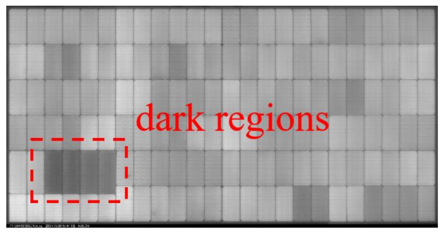
3.3. The Phenomenon of Bright and Dark Regions in Solar Modules

Solar cells processed by current injection need to be assembled into half-cell modules through laser slicing, sorting, infrared soldering, stacking, laminating, framing, etc. Infrared soldering can cause the surface of solar cells to be exposed to light and heat. Based on previous research [4,22,23], the presence of light and heat can lead to the LeTID effect, so it can be speculated that soldering would cause the LeTID effect. Thus soldered cells may experience varying degrees of efficiency degradation. If the difference in conversion efficiency between solar cells in modules exceeds 0.5%, the phenomenon of bright and dark regions would appear, which can be seen in the EL images in Figure 4. This can lead to hot spot effects in the components, causing thermal breakdown and affecting the lifespan of the solar modules and the power generation capacity of the system. Therefore, we should limit the occurrence of this phenomenon.

3.4. A Solution to Solve the Problem of Bright and Dark Regions

To solve the problem of bright and dark regions in EL images, we developed a piece of equipment, as shown in Figure 5. The cells that are pre-treated with current injection can be placed on the first storage platform and then passed through six zones, from (a) to (f). Solar cells are preheated to 80–100 °C when passing through zone (b). And then, they pass through zone (c), in which an infrared lamp is placed. Using an infrared lamp to simulate infrared soldering, the power of the infrared lamp is 1500 W and the surface temperature of the solar cell in this area is around 220–230 °C. The residence time in this area is 6 s. Subsequently, the cells pass through the cooling zone (d) and (e). After cooling, the cells are divided into different grades according to conversion efficiency. Then, cells of the same grade are welded to the same solar modules.

3.4.1. Processing Function of the Equipment

Solar cells processed through this equipment would not be affected by soldering, as accelerated degradation and regeneration would have already been carried out. Therefore, quality problems in the normal regions and the abnormal regions of the modules because of the different efficiencies could be reduced or even avoided. This can be regarded as processing equipment in this respect. To provide a clearer explanation of the processing function of this equipment, we conducted two experiments.
On the one hand, we carried out 40 parallel experiments, soldering the cells with the same grades of conversion efficiency, processed by the equipment after current injection, in the left parallel circuit of the module. In the right parallel circuit, we soldered the cells with the same grades as above but not processed by our equipment. Each piece of experiment had 36 full cells processed by our equipment and 36 full cells unprocessed by our equipment, all of which were sliced into 72 half cells by the laser. Some of the EL images had dark regions in the right parallel circuit, as shown in Figure 6. Based on our extensive experimental results, there was a 10% probability that the right parallel circuit would present bright and dark regions. However, the probability of the left was 2%. In other words, our equipment can effectively solve the problem of bright and dark regions.
On the other hand, we took individual wafers with the same grade conversion efficiency and the same material to full modules according to the half-size cell encapsulation process, calculating the theoretical power of the components and testing the actual power of the components. The power of the modules consisting of cells treated with the different pretreatment processes is shown in Table 1. In each case, 10 modules were prepared. From the results, we can see that the modules composed of solar cells processed by our equipment had higher CTM values than others, approximately 0.4%.

3.4.2. Inspection Function of the Equipment

In addition, it can also be regarded as inspection equipment. In the previous work, we could only test the quality problems of solar cells by current-induced degradation, light-induced degradation or even by observing the phenomenon of bright and dark regions directly in the modules. The means mentioned above could only be used for sampling testing, and only five batteries could be tested within 5 h, which was not only time-consuming but also highly random. However, now, our equipment can detect 60 solar cells in 1 min, which means it can detect many cells in a relatively short time. The data in Table 2 are ten sets of data randomly selected from batch testing experiment, and the total number of cells inspected by our equipment was 10,000 pieces. The degradation ratio of two of them exceeded 1%, which indicates that they were unqualified solar cells. The unqualified solar cells may have had excessive carbon or oxygen content.

3.5. Accelerated Degradation and Regeneration Mechanism of the Equipment

Figure 7 shows the mechanism of the accelerated degradation and regeneration of our equipment. For a fired solar cell, a large amount of hydrogen is trapped or stored in the silicon bulk, sometimes with weak bonds forming B–H pairs or H2 dimers [24]. Under lighting and heating conditions (≥70 °C, 1 sun) these bonds are broken, and thus, the mobile hydrogen (H0) is released [25,26]. Meanwhile, the H0 inside the silicon wafer is suspected to form a recombination-active defect with other impurities (H0-X), the X of which may be metal impurities such as Fe, Ni, Co [27,28] or intrinsic lattice defects [29], converting the solar cell from state one to state two. In addition, the out-diffusing of H0 and H2 dimers towards the surface happens simultaneously, thus lowering the concentration of hydrogen inside the silicon bulk. Under long-term photothermal conditions, to achieve a balance between H0 and H0-X, the H0-X defects inside the silicon wafer undergo dissociation, thereby transforming the solar cell from state two to state three. To date, there is still no way to directly transform solar cells from state one to state three. By accelerating degradation and regeneration, we developed equipment with lighting and heating means, which can quickly make solar cells achieve an equilibrium state of degradation and regeneration in a short period.

4. Conclusions

In this work, cells were injected with currents at an annealing temperature of 185 °C, with an injected current of 11 A and at an injection time of 770 s. Compared with the cells without any pretreatment, the relative changes in the η, Voc, Isc and FF of the cells pretreated with the optimal conditions mentioned above were 0.23%, 0.08%, 0.02% and 0.08% larger, respectively, after 25 h of degradation. Furthermore, a piece of equipment with the function of processing and inspection was developed by our team. Once the solar cells were processed by this equipment, the probability of the occurrence of that problem was estimated to be reduced from 10% to 2%, and the CTM value would increase by 0.4%. Finally, a balance mechanism between H0 and H0-X has been proposed to explain the mechanism of the equipment. The above results showed that our developed equipment has great potential for mass PERC module production. In the future, we should adjust our equipment to further improve the CTM value and apply the equipment to n-type solar cells, such as TOPCon, HJT and IBC.

Author Contributions

Conceptualization, W.F. and H.S.; methodology, W.F.; validation, W.F., X.Z. and H.P.; formal analysis, W.F.; investigation, W.F.; resources, W.F.; data curation, X.Z. and H.P.; writing—original draft preparation, W.F.; writing—review and editing, W.F., X.Z. and H.P.; visualization, H.S.; supervision, H.S.; project administration, H.S.; funding acquisition, H.S. All authors have read and agreed to the published version of the manuscript.

Funding

This work was supported by the National Natural Science Foundation of China (61774084), the Special Fund of Jiangsu Province for the Transformation of Scientific and Technological Achievements (BA2022204) and the Double Carbon Special Fund of Jiangsu Province (BE2022006).

Data Availability Statement

The original contributions presented in the study are included in the article, further inquiries can be directed to the corresponding author.

Conflicts of Interest

The authors declare no conflict of interest. Weitao Fan, Xin Zhang and Hong Pan are employees of Ycergy (Suzhou) Technology Co., Ltd. The paper reflects the views of the scientists, and not the company. Author Honglie Shen was employed by the Jiangxi HAC General Semitech Co., Ltd. The remaining authors declare that the research was conducted in the absence of any commercial or financial relationships that could be construed as a potential conflict of interest.

References

  1. Fischer, H.; Pschunder, W. Investigation of photon and thermal induced changes in silicon solar cells. In Proceedings of the 10th IEEE PVSC, Paolo Alto, CA, USA, 13–15 November 1973; pp. 404–411. [Google Scholar]
  2. Lindroos, J.; Savin, H. Review of light-induced degradation in crystalline silicon solar cells. Sol. Energy Mater. Sol. Cells 2016, 147, 115–126. [Google Scholar] [CrossRef]
  3. Ramspeck, K.; Zimmermann, S.; Nagel, H.; Metz, A.; Seidl, A. Light Induced Degradation of Rear Passivated mc-Si Solar Cells. In Proceedings of the 27th European Photovoltaic Solar Energy Conference and Exhibition, Frankfurt, Germany, 24–28 September 2012; pp. 861–865. [Google Scholar]
  4. Kersten, F.; Engelhart, P.; Ploigt, H.C.; Stekolnikov, A.; Lindner, T.; Stenzel, F.; Bartzsch, M.; Szpeth, A. A new mc-Si degradation effect called LeTID. In Proceedings of the IEEE 42nd Photovoltaic Specialist Conference 2015, New Orleans, LA, USA, 14–19 June 2015. [Google Scholar]
  5. Ning, L.T.; Song, L.H.; Zhang, J. Research progress of light and elevated temperature-induced degradation in silicon solar cells: A review. J. Alloys Compd. 2022, 912, 165120. [Google Scholar] [CrossRef]
  6. Kersten, F.; Engelhart, P.; Ploigt, H.; Stekolnikov, A.; Lindner, T.; Stenzel, F.; Bartzsch, M. Degradation of multicrystalline silicon solar cells and modules after illumination at elevated temperature. Sol. Energy Mater. Sol. Cells 2015, 142, 83–86. [Google Scholar] [CrossRef]
  7. Sio, H.C.; Wang, H.; Wang, Q.; Sun, C.; Chen, W.; Jin, H.; Macdonald, D. Light and elevated temperature induced degradation in p-type and n-type cast-grown multicrystalline and mono-like silicon. Sol. Energy Mater. Sol. Cells 2018, 182, 98–104. [Google Scholar] [CrossRef]
  8. Chen, D.; Kim, M.; Stefani, B.V.; Hallam, B.J.; Abbott, M.D.; Chan, C.E. Evidence of an identical firing-activated carrier-induced defect in monocrystalline and multicrystalline silicon. Sol. Energy Mater. Sol. Cells 2017, 172, 293–300. [Google Scholar] [CrossRef]
  9. Fritz, J.M.; Zuschlag, A.; Skorka, D. Temperature dependent degradation and regeneration of differently doped mc-Si materials. Energy Procedia 2017, 124, 718–725. [Google Scholar] [CrossRef]
  10. Fertig, F.; Lantzsch, R.; Mohr, A.; Schaper, M.; Bartzsch, M.; Wissen, D.; Kersten, F. Mass production of p-type Cz silicon solar cells approaching average stable conversion efficiencies of 22%. Energy Procedia 2017, 124, 338–345. [Google Scholar] [CrossRef]
  11. Chen, D.; Contreras, M.V.; Ciesla, A.; Hamer, P.; Hallam, B.; Abbott, M.; Chan, C. Progress in the understanding of light- and elevated temperature-induced degradation in silicon solar cells: A review. Prog. Photovolt. Res. Appl. 2021, 29, 1180–1201. [Google Scholar] [CrossRef]
  12. Yang, H.; Wang, H.; Cao, D.Y. Investigation of soldering for crystalline silicon solar cells. Solder. Surf. Mt. Technol. 2016, 28, 222–226. [Google Scholar] [CrossRef]
  13. Yang, H.; Wang, H.; Cao, D.Y.; Sun, D.M.; Ju, X.B. Analysis of Power Loss for Crystalline Silicon Solar Module during the Course of Encapsulation. Int. J. Photoenergy 2015, 2015, 539–543. [Google Scholar] [CrossRef]
  14. Koentopp, M.B.; Schutze, M.; Buβ, D.; Seguin, R. Optimized module design: A study of encapsulation losses and the influence of design parameters on module performance. IEEE J. Photovolt. 2013, 3, 138–142. [Google Scholar] [CrossRef]
  15. Philipps, S. Photovoltaics Report; Fraunhofer ISE and Werner Warmuth: Freiburg, Germany, 2023. [Google Scholar]
  16. Hanifi, H.; Pfau, C.; Dassler, D.; Schindler, S.; Schneider, J.; Turek, M.; Bagdahn, J. Ivestigation of cell-to module (CTM) ratios of PV modules by analysis of loss and gain mechanisms. Photovolt. Int. 2016, 5, 89–99. [Google Scholar]
  17. Ballif, C.; Haug, F.; Boccard, M.; Verlinden, P.; Hahn, G. Status and perspectives of crystalline silicon photovoltaics in research and industry. Nat. Rev. Mater. 2022, 7, 597–616. [Google Scholar] [CrossRef]
  18. Hanifi, H.; Dassler, D.; Turek, M.; Schneider, J. Evaluation and comparision of PV modules with different designs of partial cells in desert and moderate climates. IEEE J. Photovolt. 2018, 8, 1266–1273. [Google Scholar] [CrossRef]
  19. Hu, Z.H.; Song, L.H.; Lin, D.H.; Zhao, T.; He, Q.Y.; Yuan, S.; Yu, X.G.; Yang, D. The effect and mechanism of current injection to suppress light and elevated temperature induced degradation in p-type cast-mono and multicrystalline silicon Passivated Emitter and Rear cells. Sol. Energy 2022, 235, 12–18. [Google Scholar] [CrossRef]
  20. Hu, Z.C.; He, Q.Y.; Yuan, S.; Lin, D.H.; Song, L.H.; Yu, X.G.; Yang, D. Kinetics study on carrier injection-induced degradation and regeneration at elevated temperature in p-type cast-monosilicon passivated emitter rear contact solar cells. Sol. RRL 2021, 5, 2100035. [Google Scholar] [CrossRef]
  21. Pickett, M.D.; Buonassisi, T. Iron point defect reduction in multicrystalline silicon solar cells. Appl. Phys. Lett. 2008, 92, 122103. [Google Scholar] [CrossRef]
  22. Kersten, F.; Fertig, F.; Petter, K.; Kloter, B.; Herzog, E.; Strobel, M.B.; Heitmann, J.; Muller, J.W. System performance loss due to LeTID. Energy Procedia 2017, 124, 540–546. [Google Scholar] [CrossRef]
  23. Jafari, S.; Varshney, U.; Hoex, B.; Meyer, S.; Lausch, D. Understanding light- and elevated temperature-induced degradation in silicon wafers using hydrogen effusion mass spectroscopy. IEEE J. Photovolt. 2021, 11, 1363–1369. [Google Scholar] [CrossRef]
  24. Lin, D.H.; Hu, Z.C.; He, Q.Y.; Yang, D.; Song, L.H.; Yu, X.G. New insights on LeTID/BO-LID in p-type mono-crystalline silicon. Sol. Energy Mater. Sol. Cells 2021, 226, 111085. [Google Scholar] [CrossRef]
  25. Voronkov, V.V.; Falster, R. Formation, dissociation, and diffusion of various hydrogen dimers in silicon. Phys. Status Solidi 2017, 254, 1600779. [Google Scholar] [CrossRef]
  26. Zundel, T.; Weber, J. Boron reactivation kinetics in hydrogenated silicon after annealing in the dark or under illumination. Phys. Rev. B 1991, 43, 4361–4372. [Google Scholar] [CrossRef] [PubMed]
  27. Nakayashiki, K.; Hofstetter, J.; Morishige, A.; Li, T.; Needleman, D.B.; Jensen, M.; Buonassisi, T. Engineering solutions and root-cause analysis for light-induced degradation in p-type multicrystalline silicon PERC modules. IEEE J. Photovolt. 2016, 6, 860–868. [Google Scholar] [CrossRef]
  28. Schmidt, J.; Bredemeier, D.; Walter, D.C. On the defect physics behind light and elevated temperature-induced degradation (LeTID) of multicrystalline silicon solar cells. IEEE J. Photovolt. 2019, 9, 1497–1503. [Google Scholar] [CrossRef]
  29. Niewelt, T.; Schindler, F.; Kwapil, W.; Eberle, R.; Schon, J. Understanding the light-induced degradation at elevated temperatures: Similarities between multicrystalline and floatzone p-type silicon. Prog. Photovolt. Res. Appl. 2017, 26, 533–542. [Google Scholar] [CrossRef]
Figure 1. The results of EDE and EGE under different conditions of injection current parameters. (a) Injection current; (b) treatment temperature; (c) treatment time; (d) EL image of the solar cell after 11 A current injection at 230 °C for 700 s.
Energies 17 01550 g001
Figure 2. The relative changes in electrical performance parameters during 1 sun illumination at 85 °C. (a) Relative change in Voc; (b) relative change in Isc; (c) relative change in FF; (d) relative change in η.
Energies 17 01550 g002
Figure 3. EQE test results of the solar cells.
Energies 17 01550 g003
Figure 4. EL image of a solar module with the problem of bright and dark regions.
Energies 17 01550 g004
Figure 5. Equipment model diagram. (a) First storage platform; (b) preheating area; (c) process area; (d) first cooling area; (e) second cooling area; (f) second storage platform.
Energies 17 01550 g005
Figure 6. EL image of the module. (a) Processed by current injection firstly and equipment secondly; (b) only processed by current injection.
Energies 17 01550 g006
Figure 7. Accelerated degradation and regeneration mechanism of the equipment.
Energies 17 01550 g007
Table 1. Comparison of CTM among different modules.
SampleCase 1Case 2
Theoretical cell power (W)7.63~7.667.63~7.66
Theoretical module power (W)549.36~551.52549.36~551.52
Actual module power (W)559.91~562.69562.23~564.75
CTM ratio (%)101.9~102.1%102.3–102.5%
Case 1: modules with 144 half-size cells processed with current injection; Case 2: modules with 144 half-size cells injected with current and then processed with our equipment.
Table 2. Partial η data of batch testing before and after entering the above equipment.
Sampleη before infraredη after infraredDegradation ValueDegradation Ratio
123.2323.110.120.52%
223.3623.350.010.04%
323.3423.320.020.09%
423.3923.310.080.34%
523.4923.4900.00%
622.9722.640.331.44%
723.2522.720.532.28%
823.323.20.10.43%
923.2223.23−0.01−0.04%
1023.2723.170.10.43%
Degradation value = η before infrared—η after infrared; degradation ratio = degradation value/η before infrared.
Disclaimer/Publisher’s Note: The statements, opinions and data contained in all publications are solely those of the individual author(s) and contributor(s) and not of MDPI and/or the editor(s). MDPI and/or the editor(s) disclaim responsibility for any injury to people or property resulting from any ideas, methods, instructions or products referred to in the content.

