1. Introduction
To reduce greenhouse gas emissions and address global energy shortages, the application and development of renewable energy technologies have received widespread attention. In the process of new energy conversion, power electronics technology provides reliable technical support and has become an important component, and related technological research continues to make new progress. Elrefaey et al. introduced an enhanced topology for a DC–DC converter suitable for PV applications, with the ability to be powered by multiple DC sources and to output to multiple channels [
1]. Kulasekaran and Dasarathan focused on integrating rooftop solar with the DC microgrid and proposed a high-gain DC–DC converter for photovoltaic systems (HGBC-PVS) to connect to a higher-voltage network [
2]. A smart controller designed by A. Derrouazin based on fuzzy control was developed to oversee a sustainable hybrid power system, aiming to sustain a typical residential environment [
3]. Bodele and Kulkarni employed the bidirectional modular PV battery system (BMPBS), which utilizes non-isolated buck and boost converter combinations, to mitigate module mismatch losses due to factors such as partial shading (PS), dissimilar aging effects, different power ratings, etc. [
4].
The advancement and implementation of new energy technologies have resulted in a growing need for engineering and technical expertise in relevant industries. Within this context, creating design projects centered on power electronics technology and new energy technology holds practical significance and promotional value for enhancing the knowledge and skills of second-year college students majoring in electrical engineering. The LED street light controller based on small-scale integrated circuits integrates fundamentals of circuit and electronic technology, photovoltaic cell technology, sensing technology, and switch power supply technology. The design’s tasks and objectives encompass the following three components. The design of an energy-efficient street light intelligent controller utilizes simulator devices.
1.1. Power Module
Utilizing a lithium-ion battery, model 18650, with main parameters of 4800 mWh and 3.7 V, as the power source, the controller circuit is supplied with ±5 V DC power. When the ambient light conditions are met, the lithium battery is charged using a solar panel, selected with parameters of 5 V and 200 mA in this design.
1.2. Controller
When light is detected, the LED street light is turned off. When no light is detected, the LED street light is illuminated with low brightness, and the intensity of the low-brightness illumination can be adjusted. When someone approaches, a sound signal is detected, or a manual switch is triggered, the LED street light will illuminate at high brightness for a certain period of time, and the duration of high-brightness illumination can be adjusted.
1.3. LED Driver
The street light utilizes LED light source and requires a corresponding LED constant current driving circuit.
The remainder of the paper is organized as follows.
Section 2 will introduce the whole implement of the controller.
Section 3 will describe a simulation based on OrCAD used to verify the whole implement.
Section 4 will provide an implementation of the intelligent controller and verify availability.
2. Design of Intelligent Controller
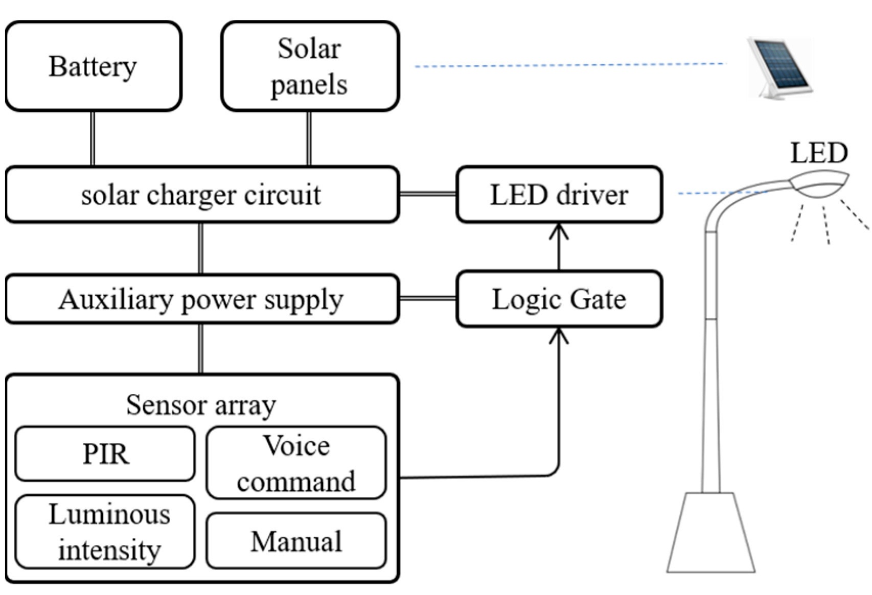
The intelligent controller’s structural diagram is depicted in
Figure 1. It primarily encompasses (1) the DC power supply unit, which furnishes DC power for detection and control circuits via DC-DC conversion. This unit comprises three modules: a boost circuit, a negative voltage generation circuit, and a battery-charging circuit [
5]. (2) The sensor detection unit comprises four modules: the light detection circuit, human infrared detection circuit, sound detection circuit, and manual switch circuit, which yield multiple logic levels. (3) The logic control unit transforms these multiple logic levels into control signals to regulate the operation, shutdown, and brightness of LED street lights. The brightness of the LED light is adjusted by the PWM modulation circuit, and the duration of high-brightness lighting is determined by the timing circuit. (4) The LED driver unit accepts the control signals and drives the LED street lights to operate with a constant current.
The organizational structure of the main circuit and the design of parameters are outlined as follows.
2.1. Passive Infra-Red Sensing Signal Processing Circuit
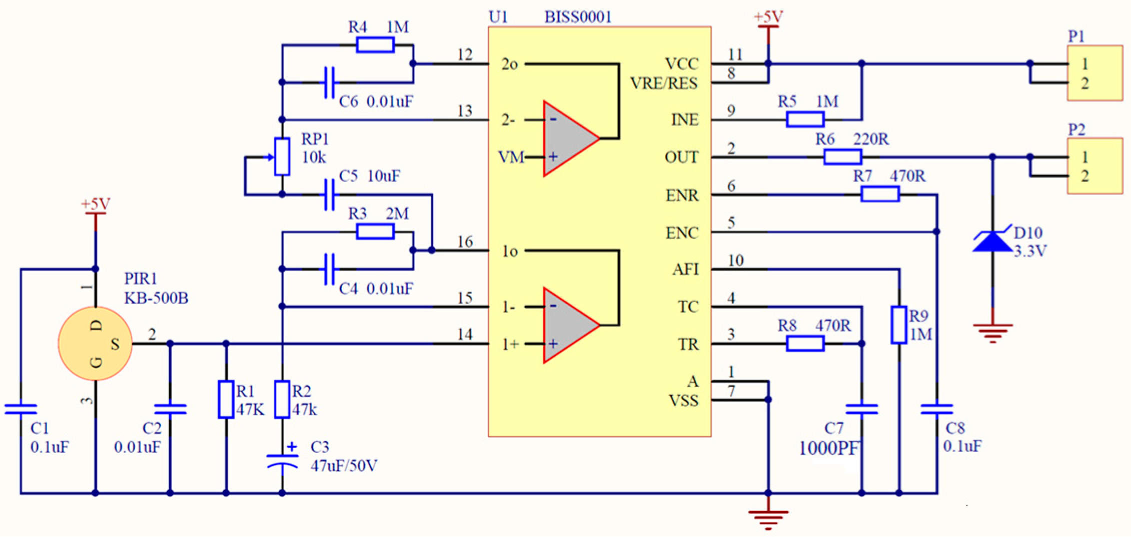
The passive infra-red (PIR) sensor, specifically the KB-500B model (Shenzhen Haiwang Sensor Co., Ltd., Shenzhen, China) chosen for this design, integrates an N-channel junction field-effect transistor in its configuration, connected using a common drain setup for impedance transformation. This converts the charge output from the pyroelectric detection element into a voltage output. Since the infrared center wavelength of human radiation falls within the 9–10 μm range, the detection element’s wavelength sensitivity spans from 0.2 to 20 μm. Typically, a window with a filter lens is positioned atop the sensor, allowing the passage of light within the 7 to 10 μm wavelength range. This facilitates the creation of an infrared sensor tailored for human radiation detection. To enhance detector sensitivity and expand the detection range, a Fresnel lens is commonly installed in front of the detector. This lens, composed of transparent plastic with equidistant tooth patterns engraved on one side, limits the incident light’s peak wavelength to approximately 10 μm. Alongside an amplification circuit, it can amplify the detection signal by over 70 dB and detect human body movement within a 20 m range [
6]. Furthermore, sensor sensitivity is influenced by the direction of human movement. Radial movement has low sensitivity, while transverse movement (i.e., perpendicular to the radius) is highly sensitive. Therefore, strategic installation positions must be selected to achieve optimal detection sensitivity.
The sensing signal is directed to a dedicated integrated circuit, with the BISS0001 [
7] selected for processing in this design. The BISS0001 comprises an operational amplifier, voltage comparator, state controller, delay time timer, blocking time timer, and reference voltage source, primarily utilized for signal amplification, control, and timing functions. As the sensor’s detection element encounters varying infrared radiation, it undergoes impedance conversion and transmits the voltage signal to the integrated circuit’s input terminal. Subsequently, it undergoes multi-stage amplification and bidirectional amplitude discrimination to identify the effective triggering signal. This then triggers a delay time timer to produce high-level pulses of a specific duration (
). Subsequently, the blocking time timer is initiated to obstruct the input end for a defined period (
) to suppress various interferences arising during the load switching process. Consequently, the detection of human infrared radiation is converted into a high-level pulse signal output.
The schematic diagram of the infrared pyroelectric sensing signal processing circuit is shown in
Figure 2. The main parameters include the following.
The first stage of voltage magnification is:
The second stage of voltage magnification is:
The total magnification can achieve 73 dB by adjusting potentiometer RP1.
The delay time of the output high level is:
The input hold-off time is:
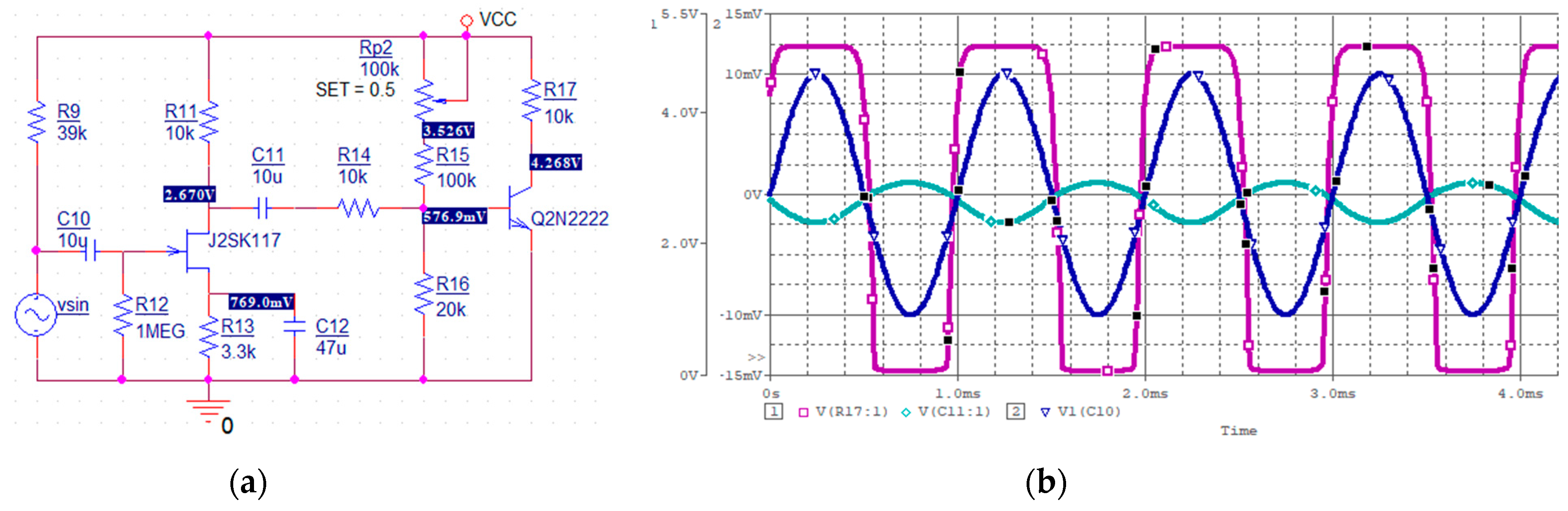
2.2. Sound Detection and Processing Circuit
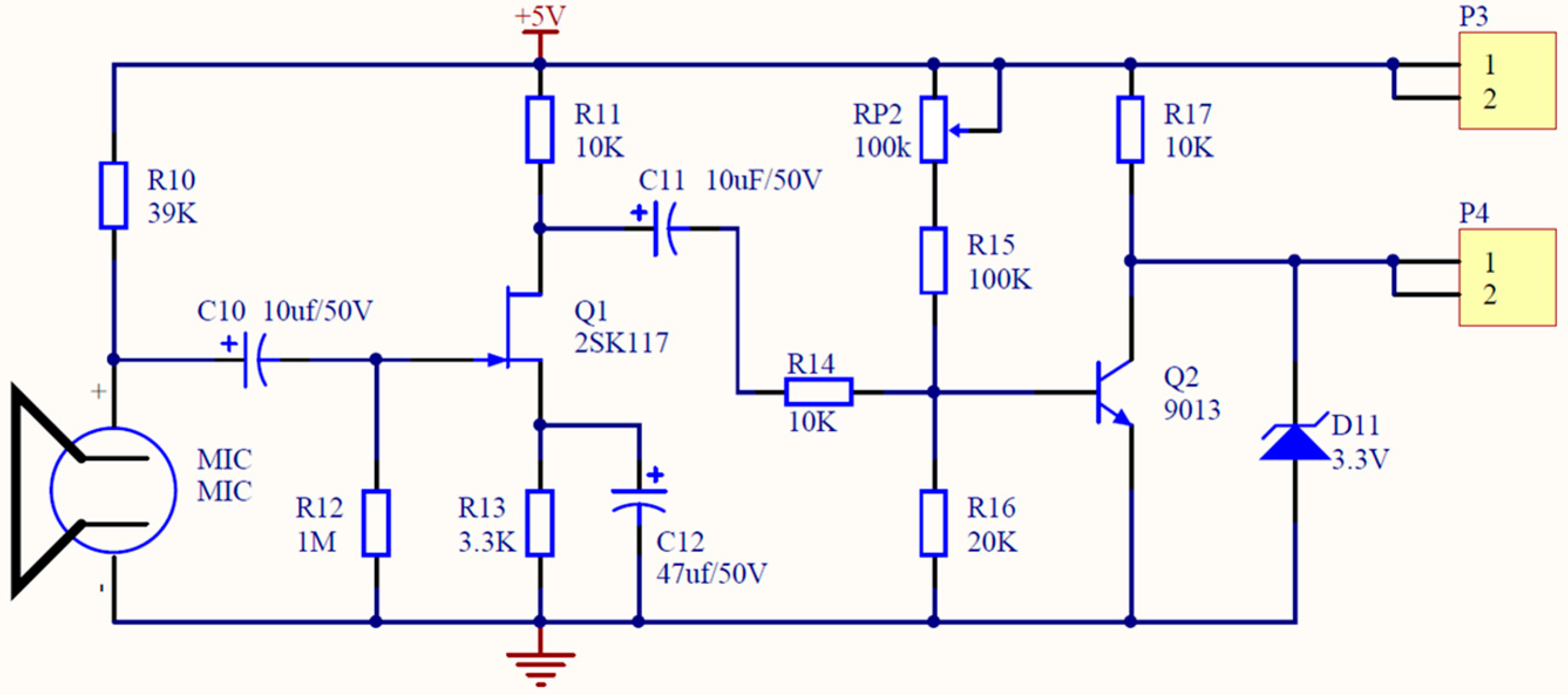
The schematic diagram depicts the operation of the sound detection and processing circuit, as shown in
Figure 3. The circuit first captures the sound signal through an electret microphone and converts it into an electrical signal. This signal is then amplified through a two-stage amplification circuit to produce a voltage signal corresponding to the sound signal.
The design incorporates an NPN transistor (model 9013 [
8]), which switches between the on/off states. Initially, it is in the cutoff region, generating a high-level output from the collector. As the microphone’s sound signal is converted into a weak electrical signal, it undergoes initial amplification through a common source amplifier circuit composed of N-channel field-effect transistors (model 2SK117 [
9]). The signal then passes through a common emitter amplifier circuit, causing the transistors to enter the saturation zone and resulting in the collector outputting a low level.
The designed parameters provide flexibility. According to the parameter calculation in the diagram, when the microphone’s output signal amplitude is 10 mV, the transistor enters the saturation zone, leading to a low-level output from the collector. During actual debugging, the potentiometer RP2 can be adjusted to set the transistor’s initial state to “cut-off”, ensuring that the collector initially outputs a high level.
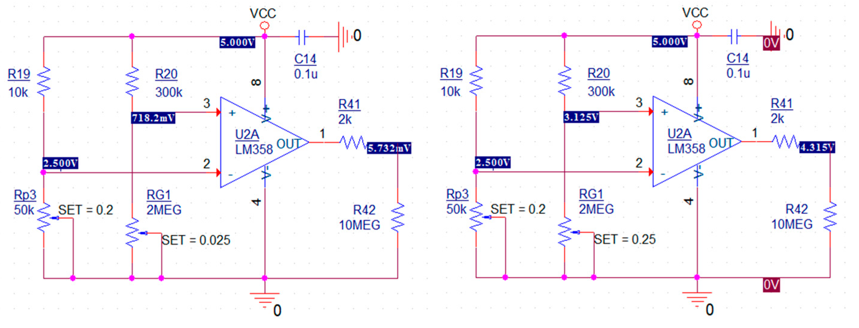
2.3. Light Detection and Processing Circuit
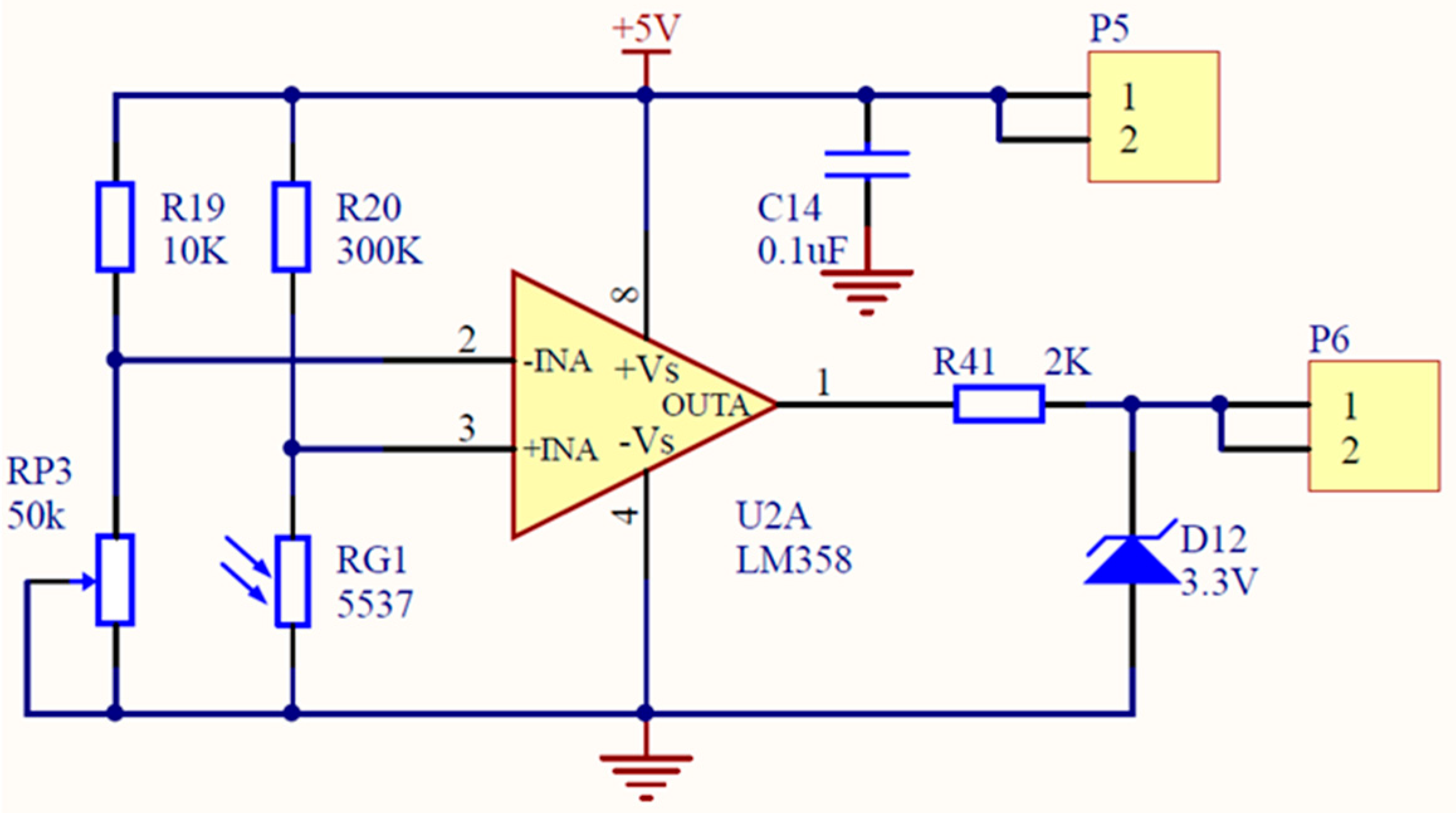
The diagram depicted in
Figure 4 illustrates the light detection and processing circuit. The main circuit consists of an in-phase voltage comparator made up of an integrated operational amplifier (specifically, model LM358 [
10] was chosen for this design). When light is present, the resistance of the photoresistor (model 5537 was used in this design) decreases, with a bright resistance of about 18–50 kΩ. This results in the input voltage of the operational amplifier dropping below the reference voltage, leading to negative saturation of the operational amplifier output. In the absence of light, the resistance value of the photoresistor increases, with a dark resistance of about 2 MΩ, causing the input voltage of the operational amplifier to surpass the reference voltage and resulting in positive saturation of the operational amplifier output. The sensitivity of the circuit to light intensity can be adjusted by manipulating potentiometer RP3.
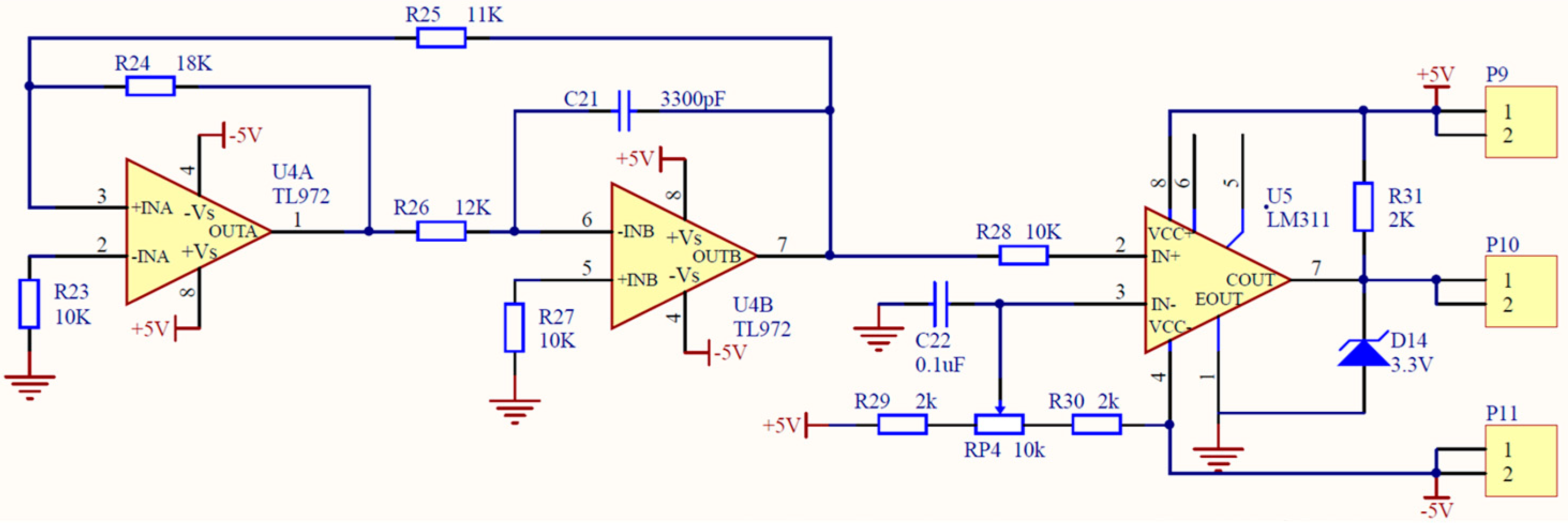
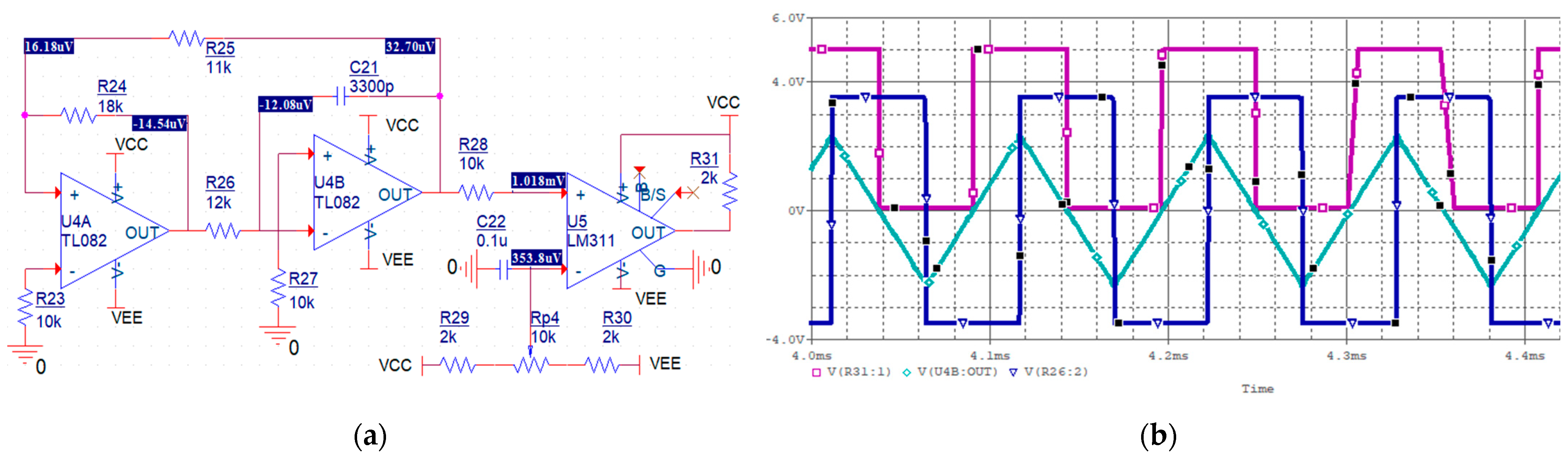
2.4. PWM Generation Circuit
The circuit of PWM generation is shown in
Figure 5. The circuit is composed of a triangular wave generator and comparator module. The triangular wave generator adopts an integral circuit structure of constant current charging and discharging to generate triangular waves with excellent linearity. The period of the triangular wave can be obtained through the following equation.
And the frequency is given by:
The amplitude of the triangular wave is:
The duty of output PWM is:
where
is the reference level of the same phase input terminal of the comparator. Adjusting the potentiometer RP4 can change the size of this value. In this scheme, the integrated operational amplifier uses TL972 [
11] and the voltage comparator uses LM311 [
12].
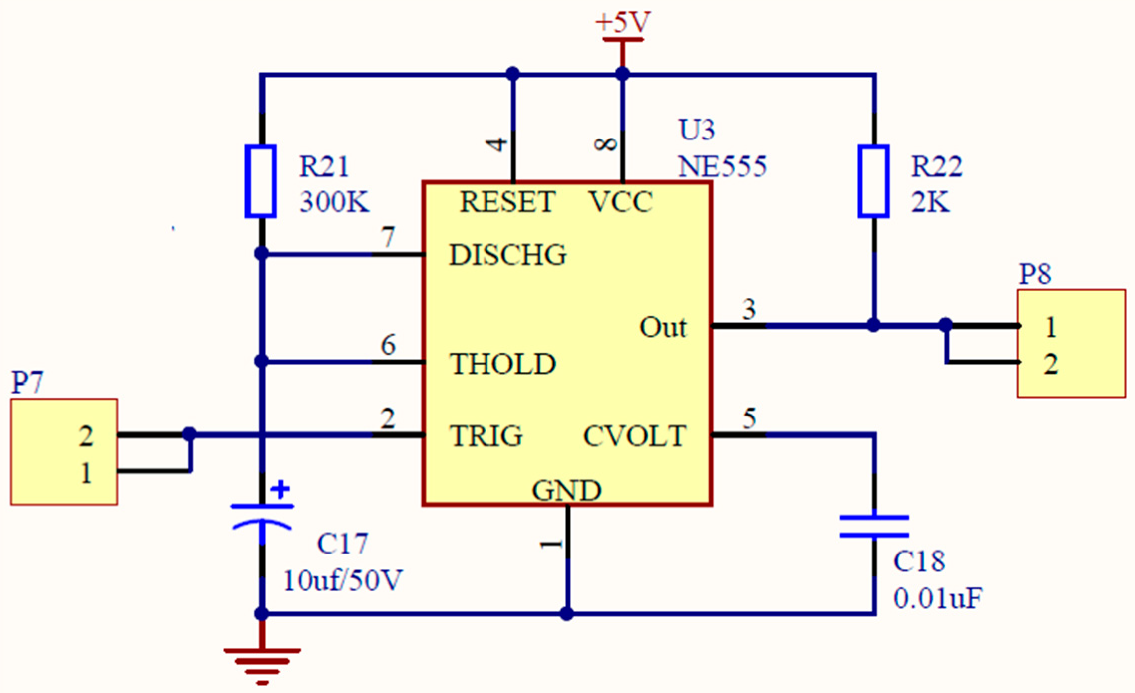
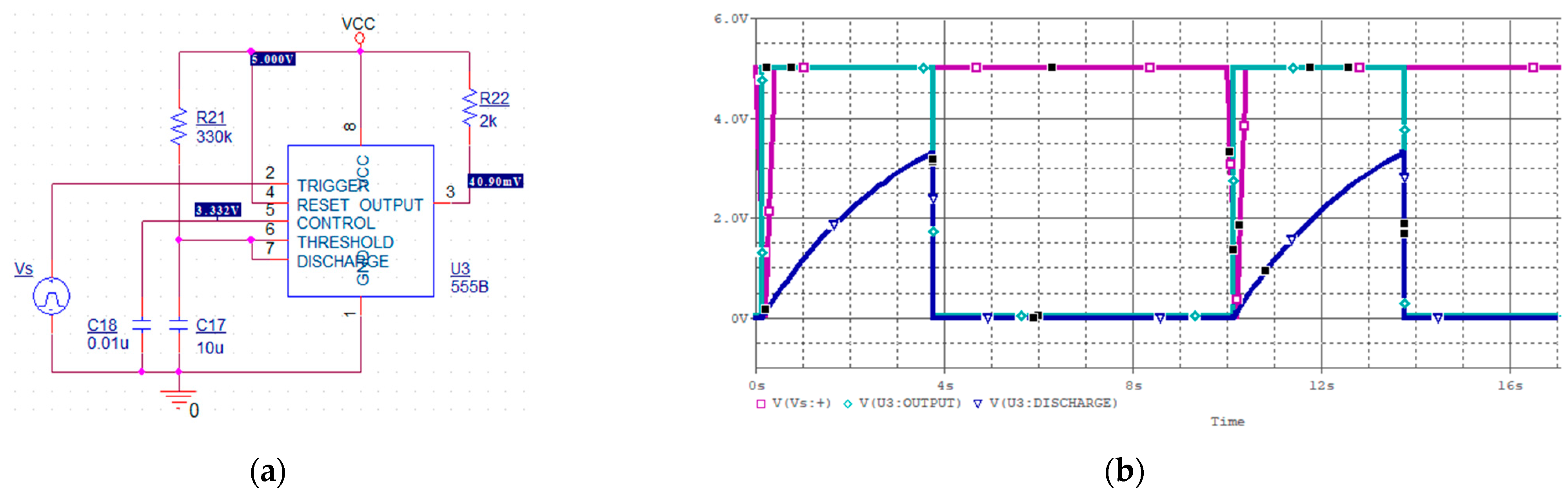
2.5. Timing Circuit
The timing circuit is utilized to produce intense illumination for a set period, employing the standard monostable circuit configuration of 555 [
13] integrated circuits. The circuit diagram is depicted in
Figure 6. The input terminal experiences a falling edge and is non-retriggerable.
The delay time is given by the following equation:
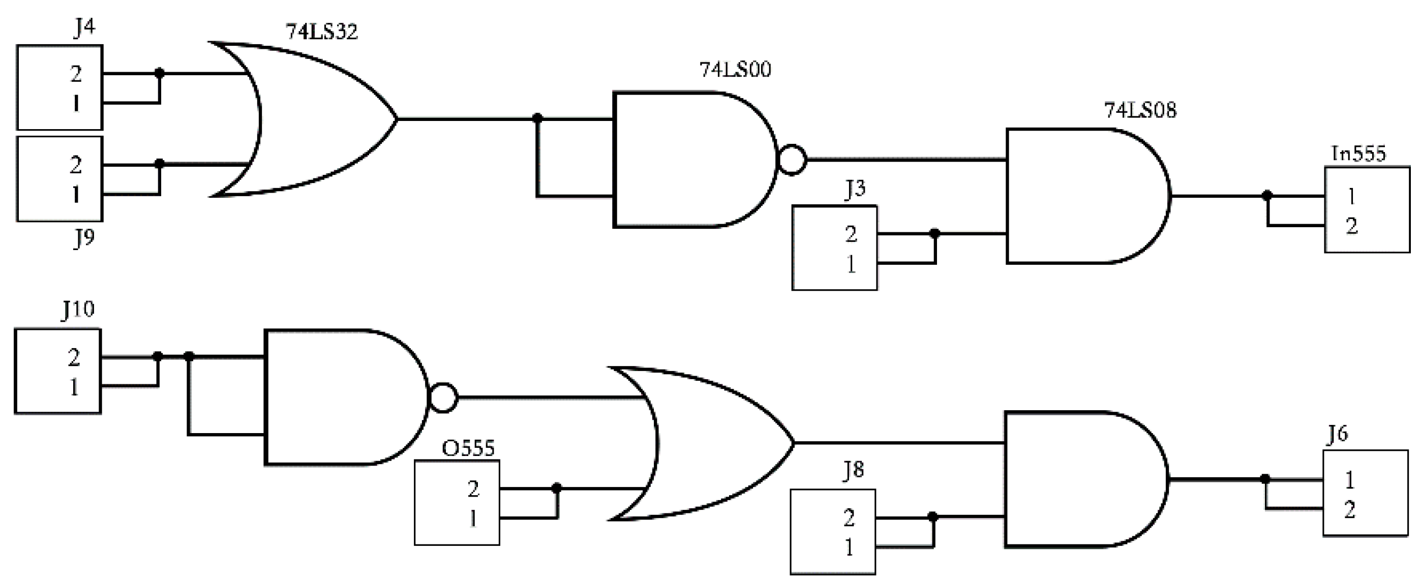
2.6. Logic Circuit
The logical circuit is the kernel of implementing intelligent control, which converts the logic level output by the multi-channel detection circuits into the control signal of the LED driver. The logical relationship is shown in
Table 1.
Logical expressions are designed according to the following requirements:
The circuit schematic diagram of this scheme using logic gate circuits 74LS00 [
14], 74LS08 [
15], and 74LS32 [
16] is shown in
Figure 7.
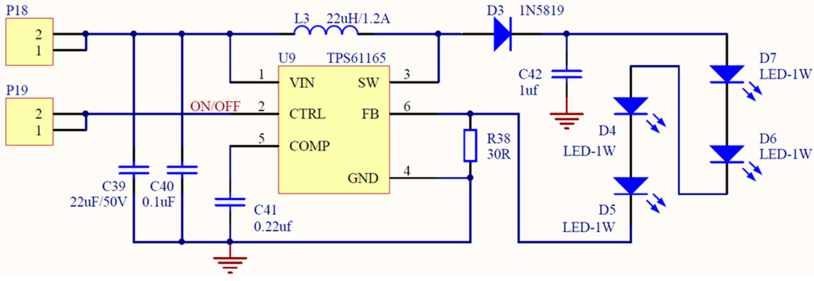
2.7. LED Driver Circuit
The schematic diagram of the LED driver circuit is shown in
Figure 8, mainly composed of a TPS61165 boost converter [
17]. By changing the input voltage of the VIN pin and the control signal of the CTRL pin, LED on/off and brightness control can be achieved.
This design load comprises a series connection of four white 1 W high-luminance (80–90 lm) LEDs, with a maximum operating current of 350 mA and a voltage of 3.0–3.4 V per LED. When the CTRL pin is held high, the reference voltage from the FB pin is 200 mV, with a 2% accuracy. The minimum value of sampling resistance is:
The driving circuit operates at a fixed switching frequency of 1.2 MHz, with a switching current limit of 1.2 A. According to
the minimum inductor is
. This design case selects an inductance value of 22 μH. Appropriately increasing the
resistance value can decrease the output current and reduce LED brightness.
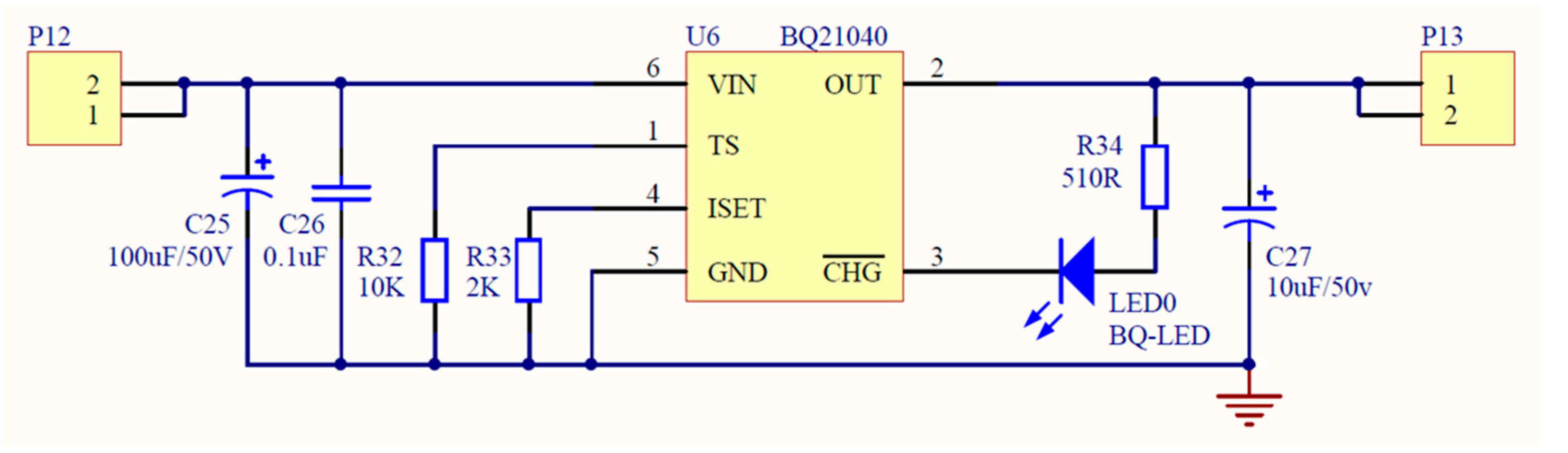
2.8. Battery Charging Circuit
The schematic diagram of the charging circuit is shown in
Figure 9. This design uses a BQ21040 integrated charger [
18] to charge lithium-ion batteries using solar panels. According to the typical parameter
in the BQ21040 data manual
, taking
, the output fast charge current can be obtained as:
Reducing the resistance value can increase the charging current, but cannot exceed the maximum continuous charging current range of lithium batteries.
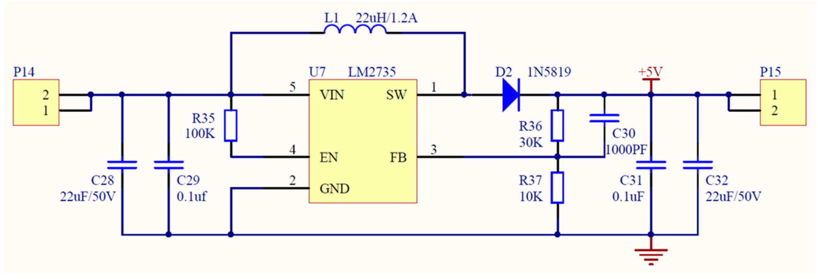
2.9. Boost Circuit
The boost circuit’s schematic diagram is depicted in
Figure 10. This design employs the LM2735 integrated circuit [
19] to elevate the DC voltage from the 3.7–4.2 V output of lithium batteries to 5 V, and accomplishes voltage stabilization. Utilizing a boost topology based on dedicated integrated circuits enables boost conversion to be achieved under voltage closed-loop feedback control.
According to the reference voltage
provided in the LM2735 data manual, the sampling voltage divider resistor can be designed using the following equation.
Take , at which point the duty cycle of the boost circuit is 0.26. Based on the LM2735 data manual, the output inductance is selected as in order to keep the boost circuit operating in CCM mode.
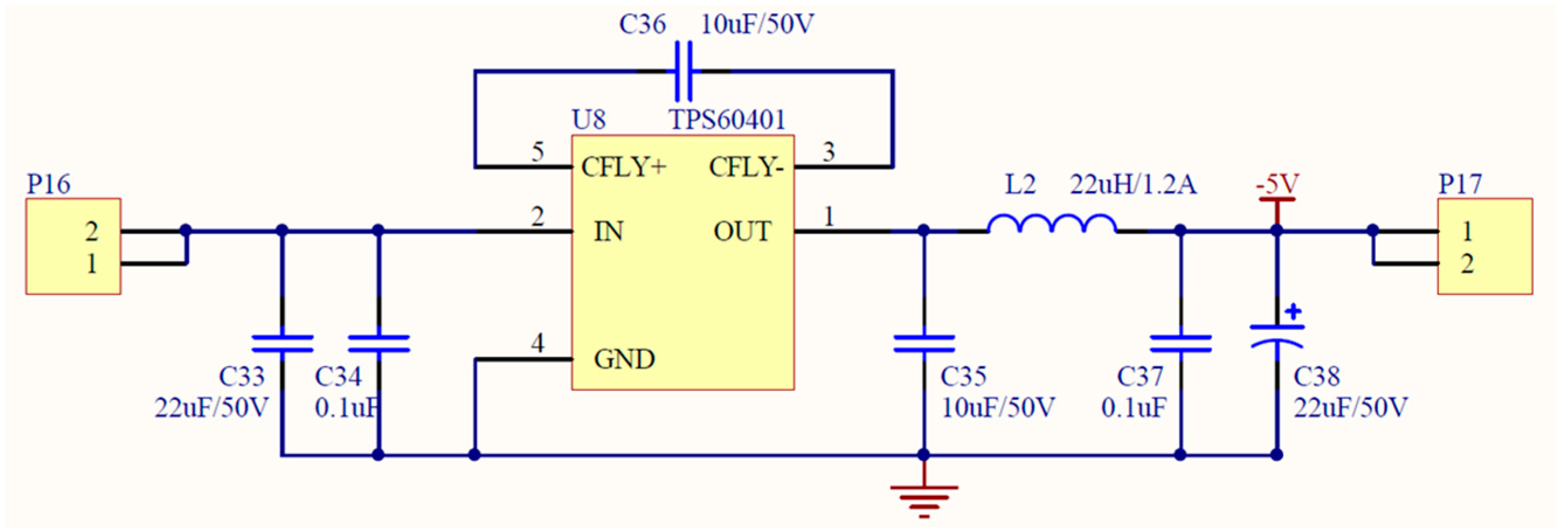
2.10. Negative Voltage Generation Circuit
The diagram in
Figure 11 illustrates the schematic of the negative voltage generation circuit. This design utilizes the TPS60401 integrated charge pump voltage converter [
20] to accomplish polarity reversal from +5 V to −5 V. Following the passage through series inductors and parallel capacitors, a stable −5 V DC voltage is produced. According to the typical parameters outlined in the TPS60401 data manual, the capacitance
is chosen as 10 μF. The fixed switching frequency is 20 kHz, and the inductance
is selected as 22 μH. The capacitance
is also chosen as 22 μF.
3. Simulation Based on OrCAD
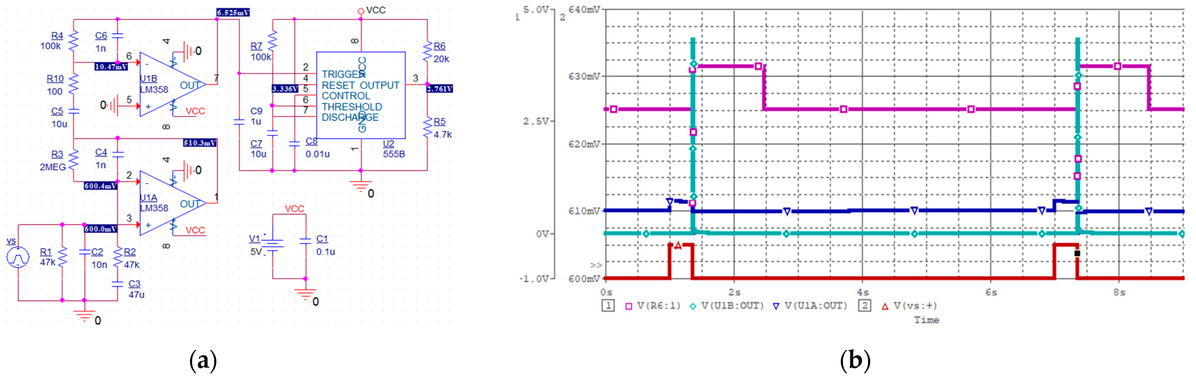
3.1. PIR Sensing Signal Processing Circuit
The parameters for the PIR sensing circuit model using LM358 and 555 are to be constructed, and both quiescent point and transient analysis are to be completed. The simulation results are displayed in
Figure 12a,b. Based on the simulation results, the PIR sensor triggers the monostable trigger inside the chip when it receives a sine signal with an offset.
3.2. Sound Detection and Processing Circuit
To create a sound detection and processing circuit based on the provided design schematic, completing both quiescent point and transient analysis is necessary. The simulation results are illustrated in
Figure 13a,b. According to the transient analysis, when the circuit receives a 10 mV, 1 kHz sine signal, the output remains in a saturated state, aligning with the design principle.
3.3. Light Detection and Processing Circuit
To construct a light detection and processing circuit based on the design schematic, we replaced the photosensitive resistor with an adjustable resistor and completed the quiescent point analysis. The simulation results are shown in
Figure 14. The analysis indicated that the circuit produces low and high output levels when the adjustable resistance values are 50 kΩ (representing illuminated) and 500 kΩ (representing non-illuminated), respectively, aligning with the design principle.
3.4. PWM Generation Circuit
To construct a PWM generation circuit based on the design schematic, we completed quiescent point analysis and transient analysis, and the simulation results are shown in
Figure 15a,b. The transient analysis revealed that the triangular wave generation circuit produces positive and negative alternating triangular waves, subsequently generating a square wave with an adjustable duty cycle amplitude of 5 V through the LM311 comparator.
3.5. Timing Circuit
To construct a timing circuit based on the design schematic, we completed quiescent point analysis and transient analysis, and the simulation results are shown in
Figure 16a,b. The transient analysis results indicate that the falling edge of the input signal triggers the timing circuit. The capacitor begins to charge, and the circuit outputs a high level with a pulse width of approximately 3.3 s. When the voltage of the capacitor reaches 3.3 V, the capacitor begins to discharge, and the circuit outputs a low level, which is consistent with the design principle.
3.6. Logic Circuit
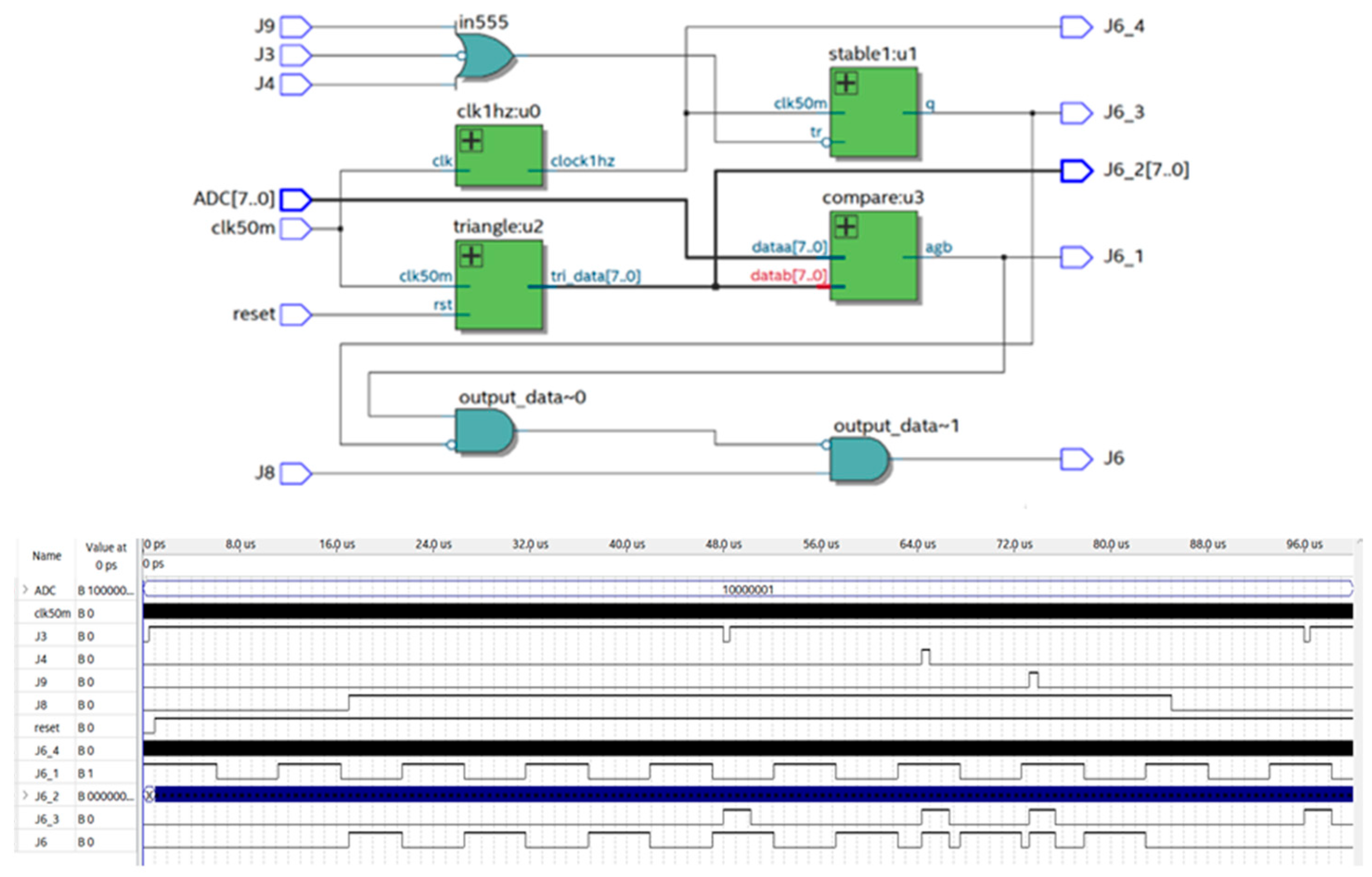
The logic circuit, as per the design schematic, utilizes the Intel MAX 10 series FPGA (model 10M50DAF484C7G [
21]). The triangular wave generator, Triangle: u2, and the ADC [7:0], as a comparator input, are employed to produce PWM waves. The simulation was conducted using ModelSim (Quartus-lite-17.1.0.590-windows), and the results are depicted in
Figure 17.
The simulation results revealed that when the light detection circuit produces a low level, the J6 output remains at a low level. When the light detection circuit outputs a high level, but the timing circuit is not triggered, J6 outputs a PWM wave, and the duty cycle can be adjusted by the ADC output, indicating adjustable brightness of the LED at low intensity. When the light detection circuit outputs a high level and triggers the timing circuit, J6 produces a high level for a specific duration determined by the timing circuit, indicating the LED’s operation at high brightness for a certain period.
4. Implementation of Controller Circuit
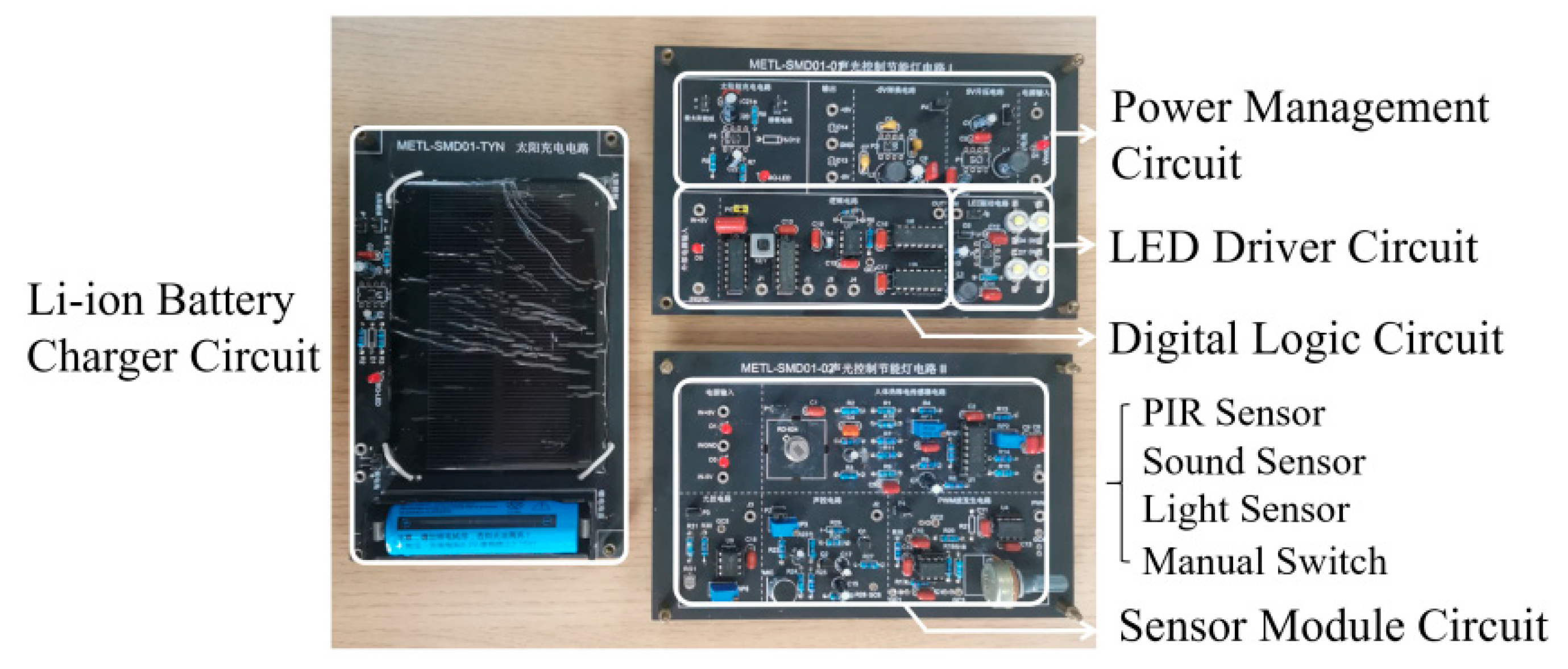
We implemented a controller testing platform as shown in
Figure 18, and based on this platform, we completed the functional and characteristic testing of the following main modules.
4.1. LED Driver Circuit
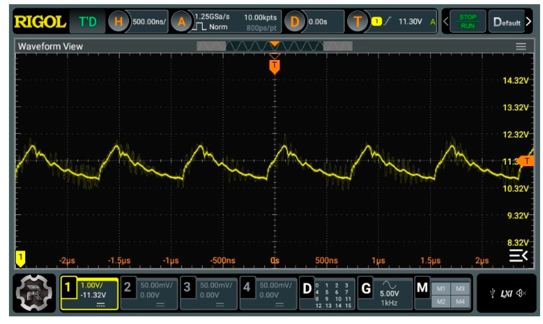
When the LED illuminated and the intensity was high, oscilloscope channel 1 was connected to the SW pin of the TPS61165 driver chip, and the waveform was observed as depicted in
Figure 19. Based on the waveform measurement, the operational frequency of the driving circuit was 1.22 MHz, and the average output voltage was 11.32 V, which is largely consistent with the intended value. During practical measurement, the sampling resistance can be set to 2 Ω, resulting in an output current of approximately 100 mA, aiming to reduce LED brightness and output power for ease of debugging.
4.2. Timing Circuit
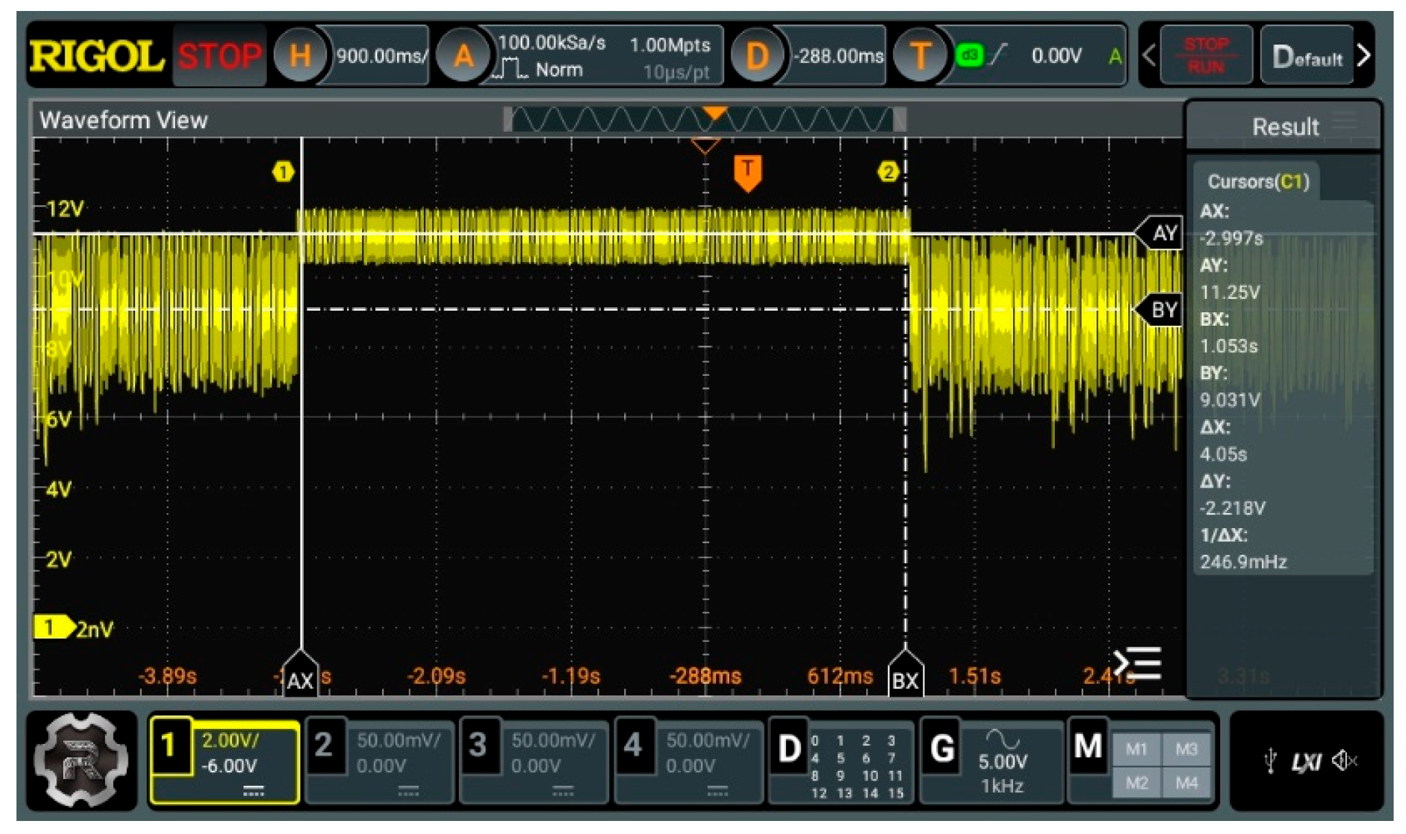
Masking the photoresistor to replicate a light-free environment causes the LED to function in a state of low-brightness illumination. The manual switch is activated, triggering the timing circuit. The process of the LED transitioning from low to high brightness, then returning to low brightness, can then be observed. The oscilloscope’s channel 1 is connected to the SW pin of the driver chip TPS61165, and the waveform is depicted in
Figure 20.
Based on waveform measurements, the average output voltage of the LED under low-brightness illumination is approximately 9.03 V, while under high-brightness illumination, the average output voltage is around 11.25 V. The duration of maintaining this value is approximately 4.05 s, with a theoretical calculation of 3.6 s, indicating an error of approximately 12%. This is primarily influenced by the precision of the selected electrolytic capacitor and resistor, which is within an acceptable range.
4.3. Sound Detection and Processing Circuit
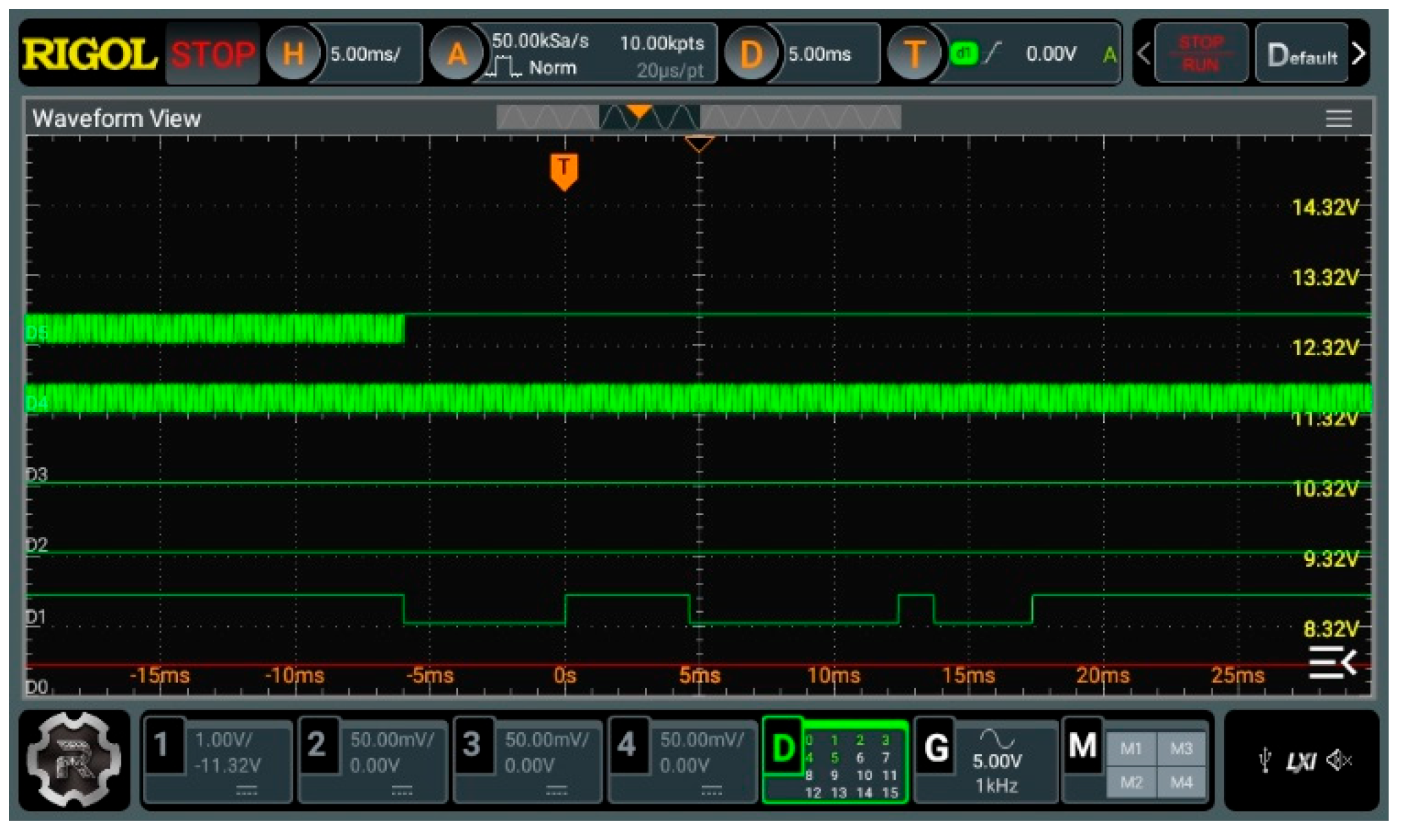
The microphone is lightly tapped to activate the sound detection circuit, causing the LED lighting brightness to transition from low to high. The output of the sound detection circuit is used as the trigger source for the oscilloscope, employing a single trigger capture. A digital logic probe is utilized to observe the output waveforms of each circuit, as illustrated in
Figure 21. In the figure, probes D0~D5, respectively, indicate the output signals of light detection, sound detection, infrared sensing, manual control, and PWM circuit, as well as the logical status of LED drive control signals.
Upon waveform observation, it is evident that when the output of the sound detection circuit shifts from a high level (silent) to a low level (audible), the LED drive control signal switches from PWM mode to high-level output mode, indicating the brightness of the LED lighting transitioning from weak to strong. As the sound is received by the microphone in wave form, it can be observed from the graph that the D1 waveform generates multiple pulses within the 25 ms range.
4.4. PIR Sensing Signal Processing Circuit
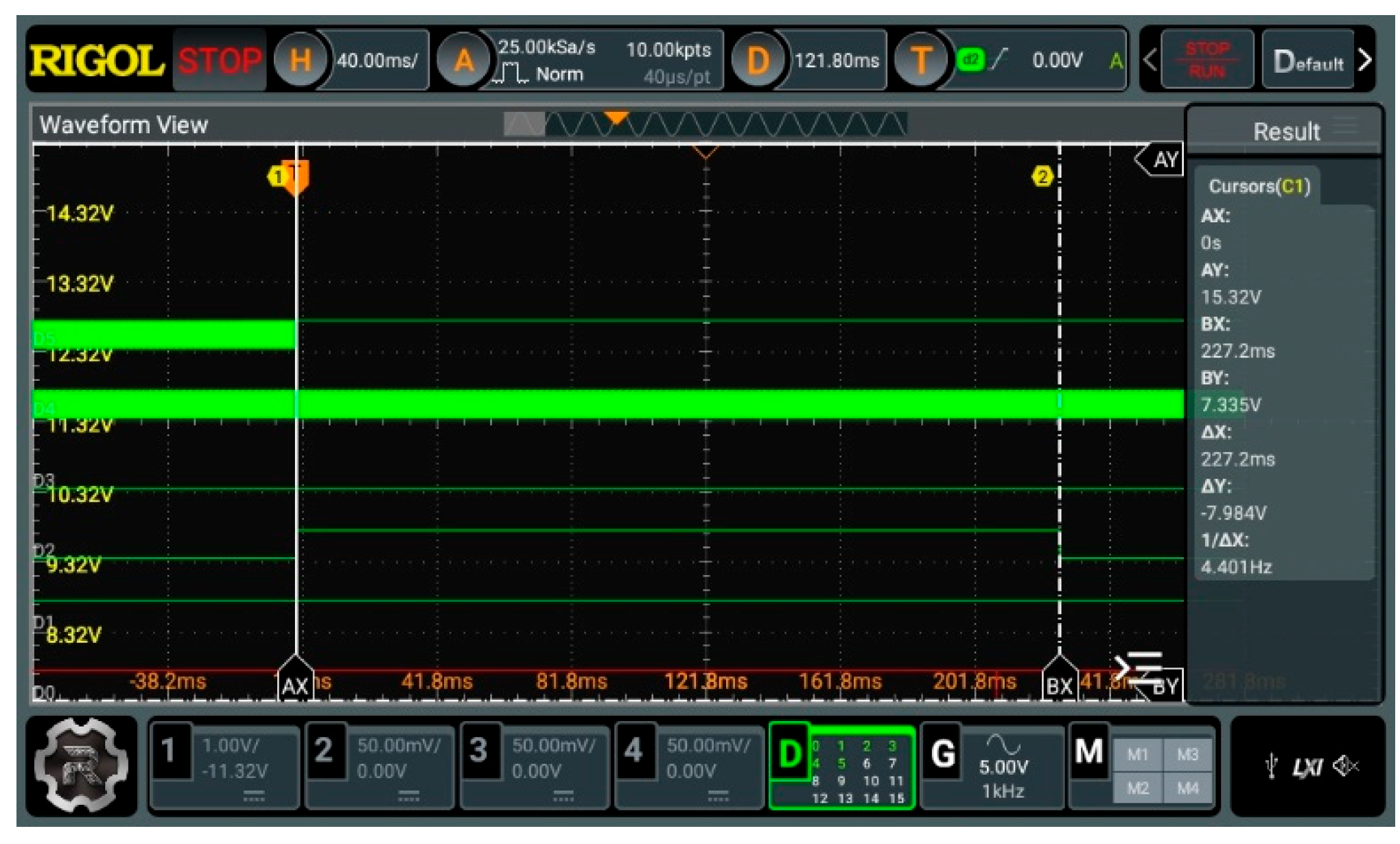
The oscilloscope logic channel connection method in
Section 4.3 is maintained. Moving the human body to effectively trigger the infrared sensing circuit, using the output of the infrared sensing circuit as the oscilloscope trigger source, and capturing the waveform with a single trigger as shown in
Figure 22 should be performed. Upon waveform observation, it is evident that when the PIR sensing circuit is triggered, a high-level pulse is generated and maintained for a period of time before returning to the low level. Using the oscilloscope cursor measurement, it can be seen that the duration of the high level is approximately 227 ms, which is consistent with the design value of 230 ms. The use of the dedicated integrated circuit BISS0001 allows for clear visibility of rising and falling edges without jitter.
4.5. Manual Switch Circuit
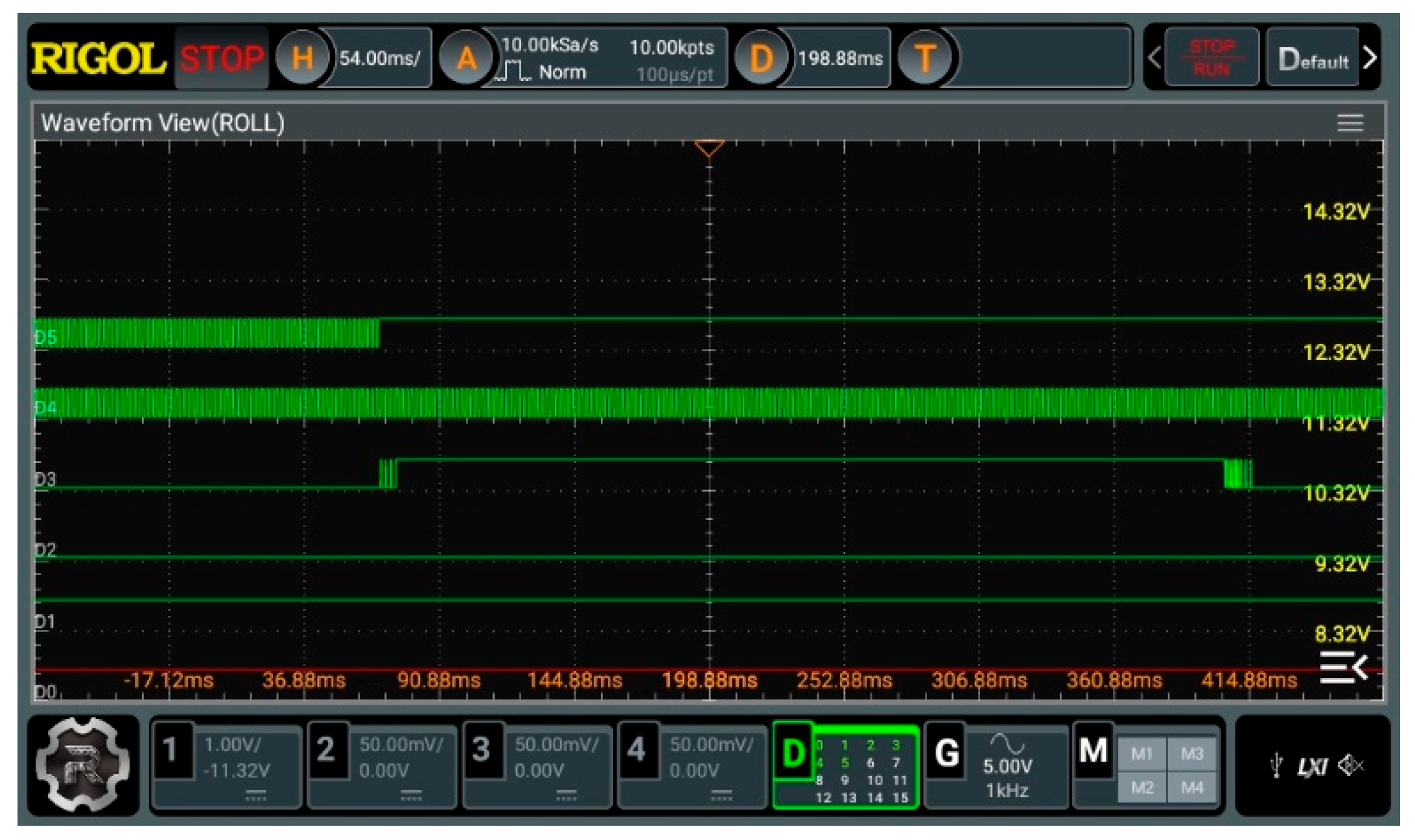
The connection method for the logic channel of the oscilloscope is maintained as described in
Section 4.3. The LED lighting brightness change is triggered manually using a switch. The switch output is used as the trigger source for the oscilloscope, and the waveform is depicted in
Figure 23.
Upon waveform observation, it is evident that when the switch is closed and opened, there will be short-term rapid fluctuations. When the first jitter occurs, the LED driver control signal is triggered to switch from PWM mode to high-level output mode, representing the brightness of the LED lighting transitioning from low to high. According to the cursor measurement results, the switch action lasted for approximately 325 ms.
4.6. Light Detection and Processing Circuit
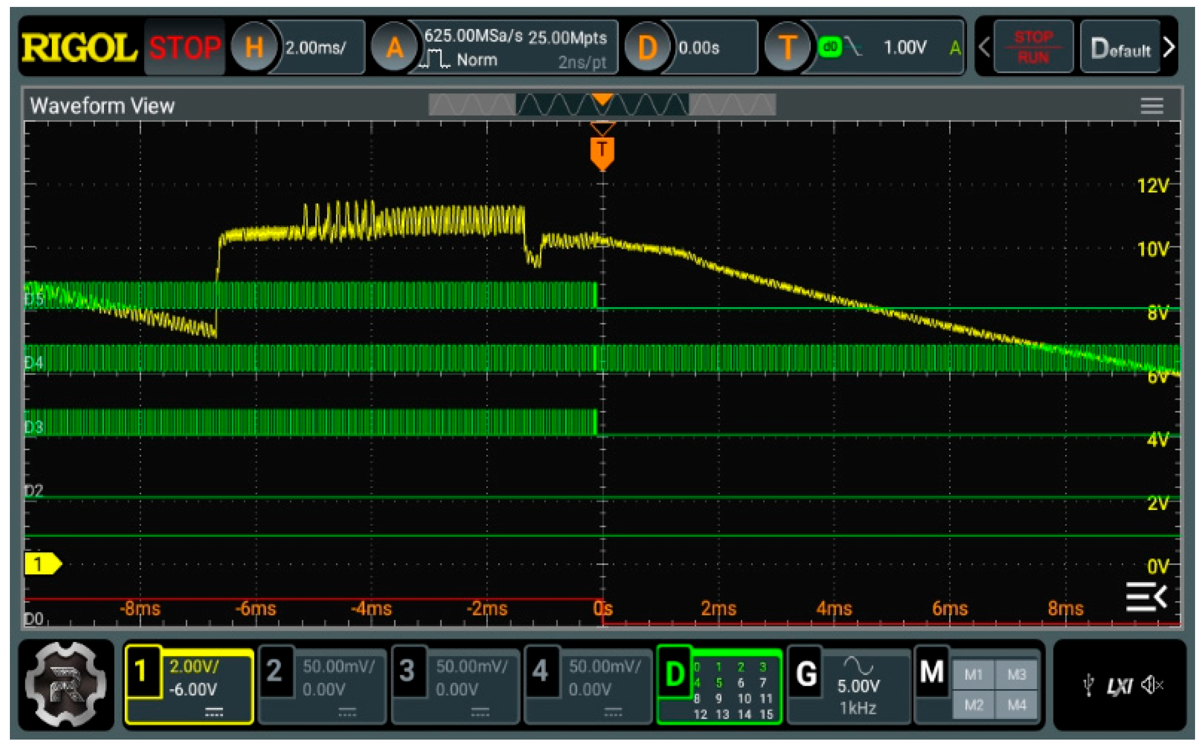
The methodology for maintaining the connection of the oscilloscope logic channel in
Section 4.3 and linking the oscilloscope analog channel CH1 to the SW pin of the LED driver chip TPS61165 should be upheld. The lighting simulation involves using a flashlight and using the output of the light control circuit as the trigger source for the oscilloscope, capturing the waveform with a single trigger, as illustrated in
Figure 24. Upon observation of the waveform, it is evident that the transition of the lighting detection circuit output from a high level (representing no illumination) to a low level (representing illumination) causes the LED driver control signal to shift from PWM mode to low-level output mode, indicating the change in the LED light’s operational state from low-brightness illumination to off. The output waveform of the oscilloscope analog channel demonstrates a gradual decrease in the output voltage of the driving circuit to 5 V as the output of the optical control circuit changes. As per the cursor measurement, the output voltage drop process in the figure takes approximately 10 ms.
The simulation and actual measurement results of the primary unit circuits affirm that the intelligent controller’s circuit functions and main performance indicators fulfill the design requirements. It can intelligently regulate the operational status of LED street light through light intensity, human infrared, sound, and manual switches, thereby achieving energy-saving effects.
5. Conclusions
This paper presents an intelligent controller of LED street light, leveraging simulator devices to enable intelligent perception, dimming, and control of LED street light across multiple channels. The design encompasses fundamental circuit principles, digital and analog electronic technology, as well as core professional courses like power electronic technology and sensor technology. The training focuses on theoretical design, EDA simulation, and experimental debugging. It also integrates the design and implementation of basic unit circuits such as digital logic circuits, BJT and MOS transistor circuits, operational amplifiers, and comparator circuits. Furthermore, it includes targeted expansion in typical applications of 555 chips and DC-DC power supply chips, with a focus on practical teaching value. By substituting and combining local unit circuits, advanced designs for this controller can be developed. For example, using FPGA technology to achieve PWM generation and control is expected to improve controller performance and development efficiency. Due to the focus of this solution on the circuit implementation of analog devices and the lack of in-depth research on FPGA applications, this will be the main research area of the team in the next stage.
Author Contributions
Conceptualization, Z.W., D.Z., and W.Z.; methodology, Z.W., D.Z., and W.Z.; software, Z.W. and J.L.; validation, J.L. and D.Z.; formal analysis, D.Z. and W.Z.; investigation, Z.W. and D.Z.; resources, W.Z.; data curation, Z.W.; writing—original draft preparation, Z.W. and J.L.; writing—review and editing, Z.W. and J.L.; visualization, Z.W. and J.L.; supervision, Z.W.; project administration, Z.W., D.Z., and W.Z. All authors have read and agreed to the published version of the manuscript.
Funding
This research received no external funding.
Data Availability Statement
The data presented in this study are all available in the article.
Conflicts of Interest
The authors declare no conflicts of interest.
References
- Elrefaey, M.S.; Ibrahim, M.E.; Eldin, E.T.; Hegazy, H.Y.; El-Kholy, E.E.; Abdalfatah, S. Multiple-source single-output buck-boost DC–DC converter with increased reliability for photovoltaic (PV) applications. Energies 2023, 16, 216. [Google Scholar] [CrossRef]
- Kulasekaran, P.S.; Dasarathan, S. Design and analysis of interleaved high-gain bi-directional DC–DC converter for microgrid application integrated with photovoltaic systems. Energies 2023, 16, 5135. [Google Scholar] [CrossRef]
- Derrouazin, A.; Aillerie, M.; Mekkakia-Maaza, N.; Charles, J.-P. Multi input-output fuzzy logic smart controller for a residential hybrid solar-wind-storage energy system. Energy Convers. Manag. 2017, 148, 238–250. [Google Scholar] [CrossRef]
- Bodele, N.J.; Kulkarni, P.S. Modular battery-integrated bidirectional single-stage DC–DC converter for solar PV based DC nano-grid application. Sol. Energy 2023, 259, 1–14. [Google Scholar] [CrossRef]
- Patel, M.; Zhou, Z. An interleaved battery charger circuit for a switched capacitor inverter-based standalone single-phase photovoltaic energy management system. Energies 2023, 16, 7155. [Google Scholar] [CrossRef]
- Urfaliglu, O.; Soyer, E.B.; Toreyin, B.U.; Cetin, A.E. PIR-sensor based human motion event classification. In Proceedings of the 2008 IEEE 16th Signal Processing, Communication and Applications Conference, Aydin, Türkiye, 20–22 April 2008; pp. 1–4. [Google Scholar]
- Micro Power PIR Motion Detector, IC. Available online: http://www.ladyada.net/media/sensors/BISS0001.pdf (accessed on 14 January 2024).
- 2N9013 Transistor. Available online: http://www.unisonic.com.tw/datasheet/9013.pdf (accessed on 14 January 2024).
- Field Effect Transistor Silicon N-Channel Junction Type 2SK117 Low Noise Audio Amplifier Applications. Available online: https://www.futurlec.com/Datasheet//Transistors/2SK117pdf (accessed on 30 January 2024).
- Industry-Standard Dual Operational Amplifiers. Available online: https://www.ti.com/lit/gpn/lm358 (accessed on 14 January 2024).
- TL97x Output Rail-To-Rail Very-Low-Noise Operational Amplifiers. Available online: https://www.ti.com/lit/gpn/tl972 (accessed on 14 January 2024).
- LM111, LM211, LM311 Differential Comparators. Available online: https://www.ti.com/lit/gpn/lm311 (accessed on 14 January 2024).
- LM555 Timer. Available online: https://www.ti.com/lit/gpn/lm555 (accessed on 14 January 2024).
- SNx400, SNx4LS00, and SNx4S00 Quadruple 2-Input Positive-NAND Gates. Available online: https://www.ti.com/lit/gpn/sn74ls00 (accessed on 14 January 2024).
- Quadruple 2-Input Positive-and Gates. Available online: https://www.ti.com/lit/gpn/sn74ls08 (accessed on 14 January 2024).
- Quadruple 2-Input Positive-or Gates. Available online: https://www.ti.com/lit/gpn/sn74ls32 (accessed on 14 January 2024).
- TPS61165 High-Brightness, White LED Driver in WSON and SOT-23 Packages. Available online: https://www.ti.com/lit/gpn/tps61165 (accessed on 14 January 2024).
- BQ21040 0.8-A, Single-Input, Single Cell Li-Ion and Li-Pol Battery Charger. Available online: https://www.ti.com/lit/gpn/bq21040 (accessed on 14 January 2024).
- LM2735 520-kHz and 1.6-MHz Space-Efficient Boost and SEPIC DC/DC Regulator. Available online: https://www.ti.com/lit/gpn/lm2735 (accessed on 14 January 2024).
- TPS6040x Unregulated 60-mA Charge Pump Voltage Inverter. Available online: https://www.ti.com/lit/gpn/tps60401 (accessed on 14 January 2024).
- Intel® MAX® 10 FPGA Device Datasheet. Available online: https://cdrdv2-public.intel.com/666319/m10_datasheet-683794-666319.pdf (accessed on 14 January 2024).
Figure 1.
Structure of intelligent controller.
Figure 1.
Structure of intelligent controller.
Figure 2.
PIR sensing signal processing circuit.
Figure 2.
PIR sensing signal processing circuit.
Figure 3.
Sound detection and processing circuit.
Figure 3.
Sound detection and processing circuit.
Figure 4.
Light detection and processing circuit.
Figure 4.
Light detection and processing circuit.
Figure 5.
PWM generation circuit.
Figure 5.
PWM generation circuit.
Figure 6.
Timing circuit.
Figure 6.
Timing circuit.
Figure 7.
Implementation of intelligent logic based on 74 Series IC.
Figure 7.
Implementation of intelligent logic based on 74 Series IC.
Figure 8.
LED driver circuit.
Figure 8.
LED driver circuit.
Figure 9.
Battery charging circuit.
Figure 9.
Battery charging circuit.
Figure 10.
Boost circuit.
Figure 10.
Boost circuit.
Figure 11.
Negative voltage generation circuit.
Figure 11.
Negative voltage generation circuit.
Figure 12.
(a) Quiescent point analysis of PIR sensing signal processing circuit; (b) transient analysis of PIR sensing signal processing circuit.
Figure 12.
(a) Quiescent point analysis of PIR sensing signal processing circuit; (b) transient analysis of PIR sensing signal processing circuit.
Figure 13.
(a) Quiescent point analysis of sound detection and processing circuit; (b) transient analysis of sound detection and processing circuit.
Figure 13.
(a) Quiescent point analysis of sound detection and processing circuit; (b) transient analysis of sound detection and processing circuit.
Figure 14.
Quiescent point analysis of light detection and processing circuit.
Figure 14.
Quiescent point analysis of light detection and processing circuit.
Figure 15.
(a) Quiescent point analysis of PWM generation circuit; (b) transient analysis of PWM generation circuit.
Figure 15.
(a) Quiescent point analysis of PWM generation circuit; (b) transient analysis of PWM generation circuit.
Figure 16.
(a) Quiescent point analysis of timing circuit; (b) transient analysis of timing circuit.
Figure 16.
(a) Quiescent point analysis of timing circuit; (b) transient analysis of timing circuit.
Figure 17.
ModelSim simulation based on Intel MAX 10 Series FPGA.
Figure 17.
ModelSim simulation based on Intel MAX 10 Series FPGA.
Figure 18.
Testing platform of intelligent controller.
Figure 18.
Testing platform of intelligent controller.
Figure 19.
SW pin of LED driver circuit.
Figure 19.
SW pin of LED driver circuit.
Figure 20.
SW pin after starting the timing circuit.
Figure 20.
SW pin after starting the timing circuit.
Figure 21.
LED control triggered by sound detection circuit.
Figure 21.
LED control triggered by sound detection circuit.
Figure 22.
LED control triggered by PIR detection circuit.
Figure 22.
LED control triggered by PIR detection circuit.
Figure 23.
LED control triggered by manual switch.
Figure 23.
LED control triggered by manual switch.
Figure 24.
LED control triggered by light detection circuit.
Figure 24.
LED control triggered by light detection circuit.
Table 1.
Port output status description.
Table 1.
Port output status description.
| Port Label | Port Source | Description |
|---|
| J3 | Sound detection circuit | If not sounds, output H level; otherwise, output L level |
| J4 | PIR sensing circuit | If no one detected, output L level; otherwise, H level |
| J9 | Manual switch | An H level is output when manual is switched, or keep L level |
| J8 | Light detection circuit | If no light, output H level, or output L level |
| J10 | PWM generation circuit | Brightness control by duty cycle |
| J6 | LED driver circuit | If obtains H level; otherwise, obtains L level |
| Disclaimer/Publisher’s Note: The statements, opinions and data contained in all publications are solely those of the individual author(s) and contributor(s) and not of MDPI and/or the editor(s). MDPI and/or the editor(s) disclaim responsibility for any injury to people or property resulting from any ideas, methods, instructions or products referred to in the content. |
© 2024 by the authors. Licensee MDPI, Basel, Switzerland. This article is an open access article distributed under the terms and conditions of the Creative Commons Attribution (CC BY) license (https://creativecommons.org/licenses/by/4.0/).


