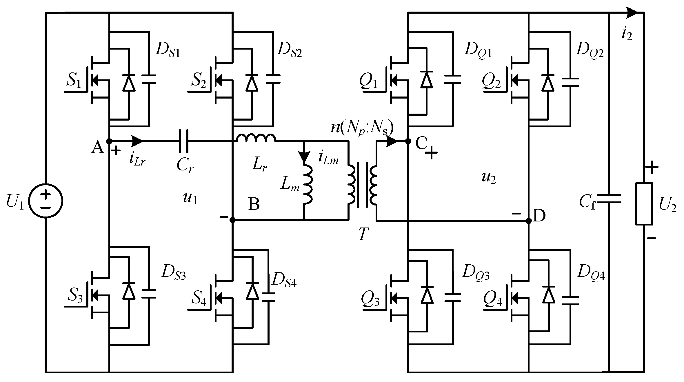
Figure 1.
Full bridge LLC resonant converter.
Figure 1.
Full bridge LLC resonant converter.
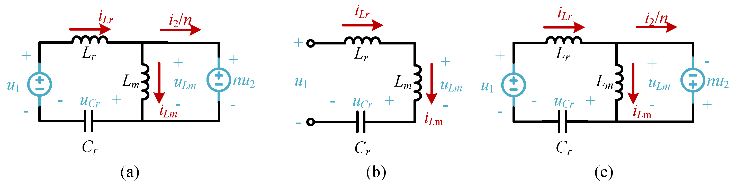
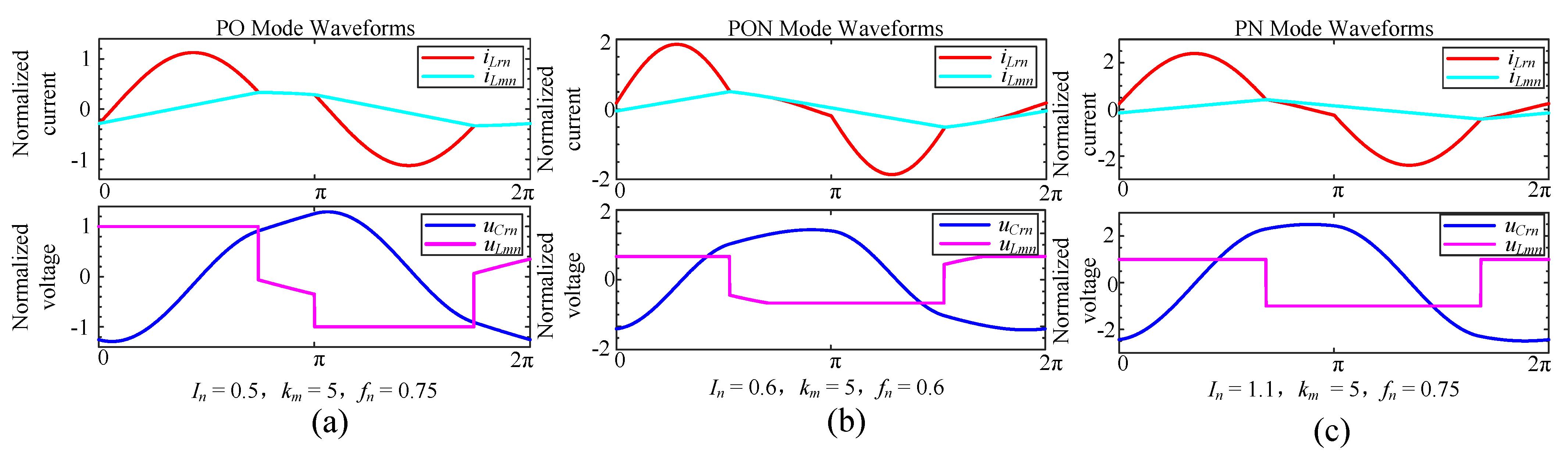
Figure 2.
Equivalent circuit of the LLC resonant tank in different operating stages. (a) P stage. (b) O stage. (c) N stage.
Figure 2.
Equivalent circuit of the LLC resonant tank in different operating stages. (a) P stage. (b) O stage. (c) N stage.
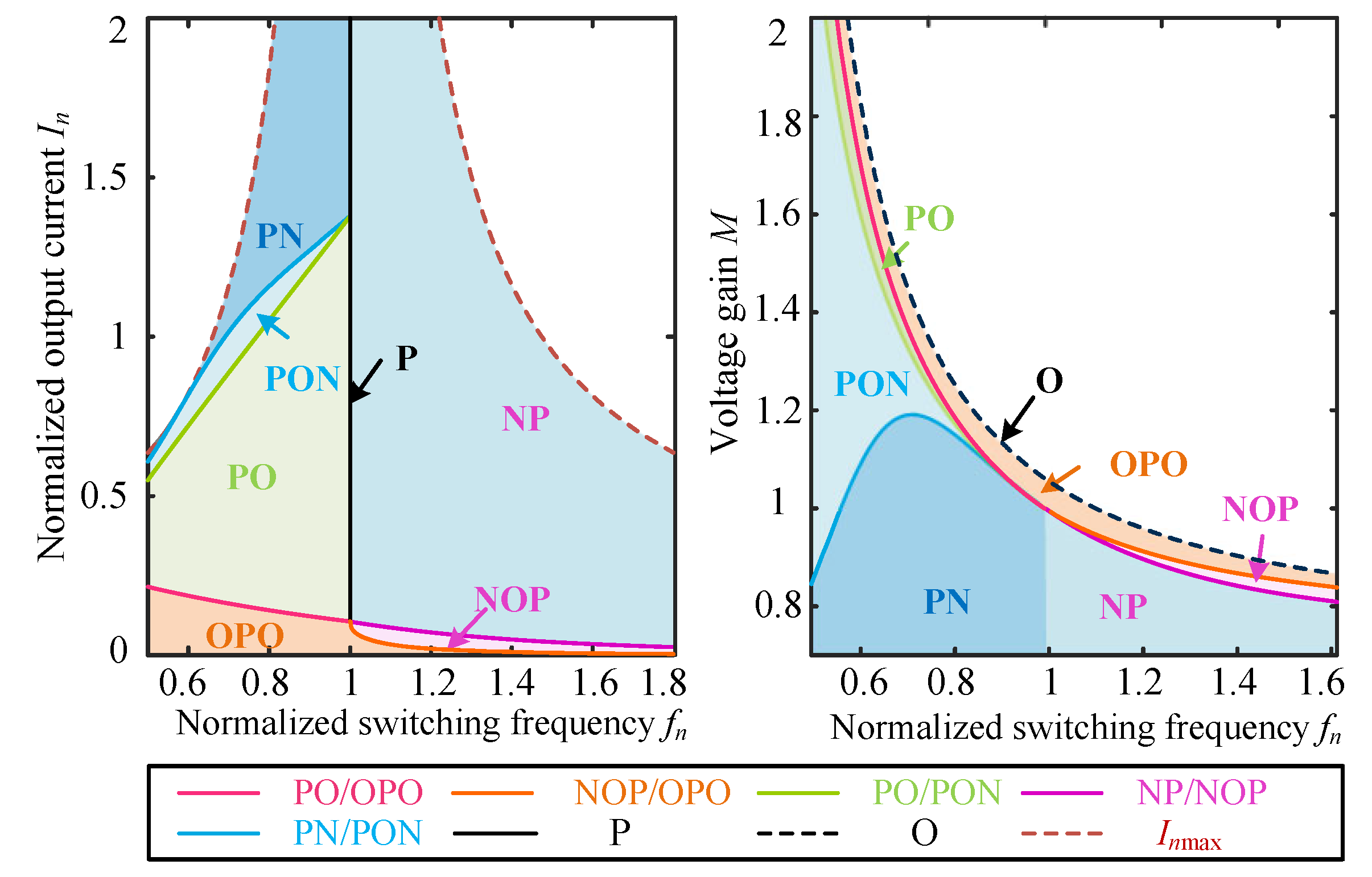
Figure 3.
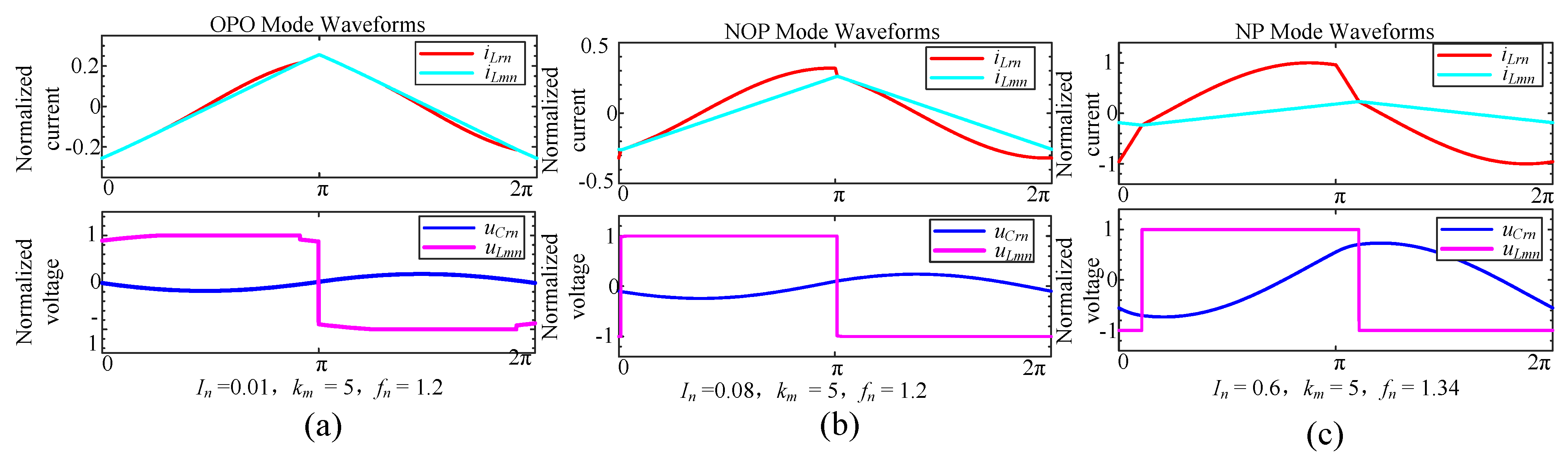
Modes distribution of LLC in - plane and -M plane.
Figure 3.
Modes distribution of LLC in - plane and -M plane.
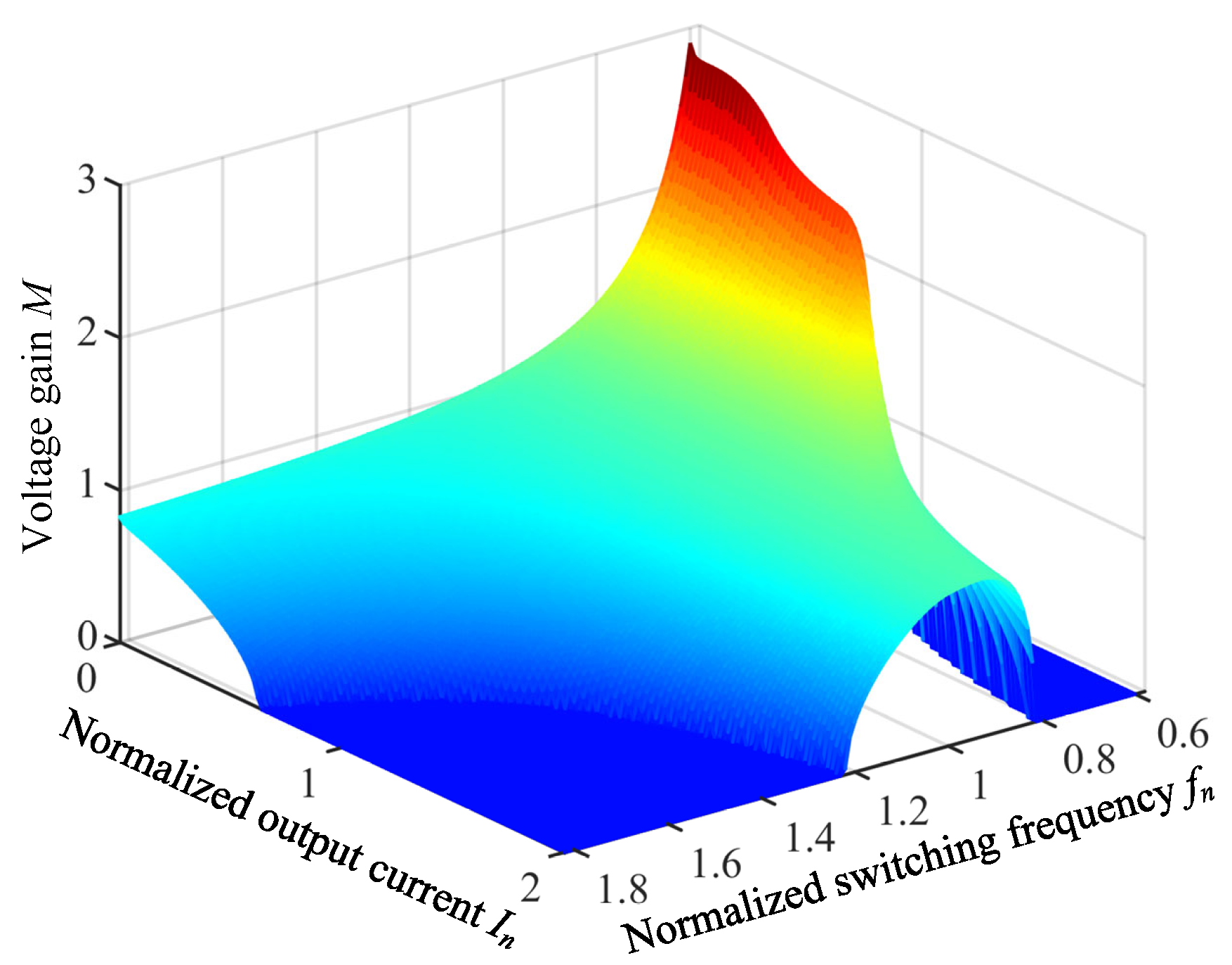
Figure 4.
Variation in with M and .
Figure 4.
Variation in with M and .
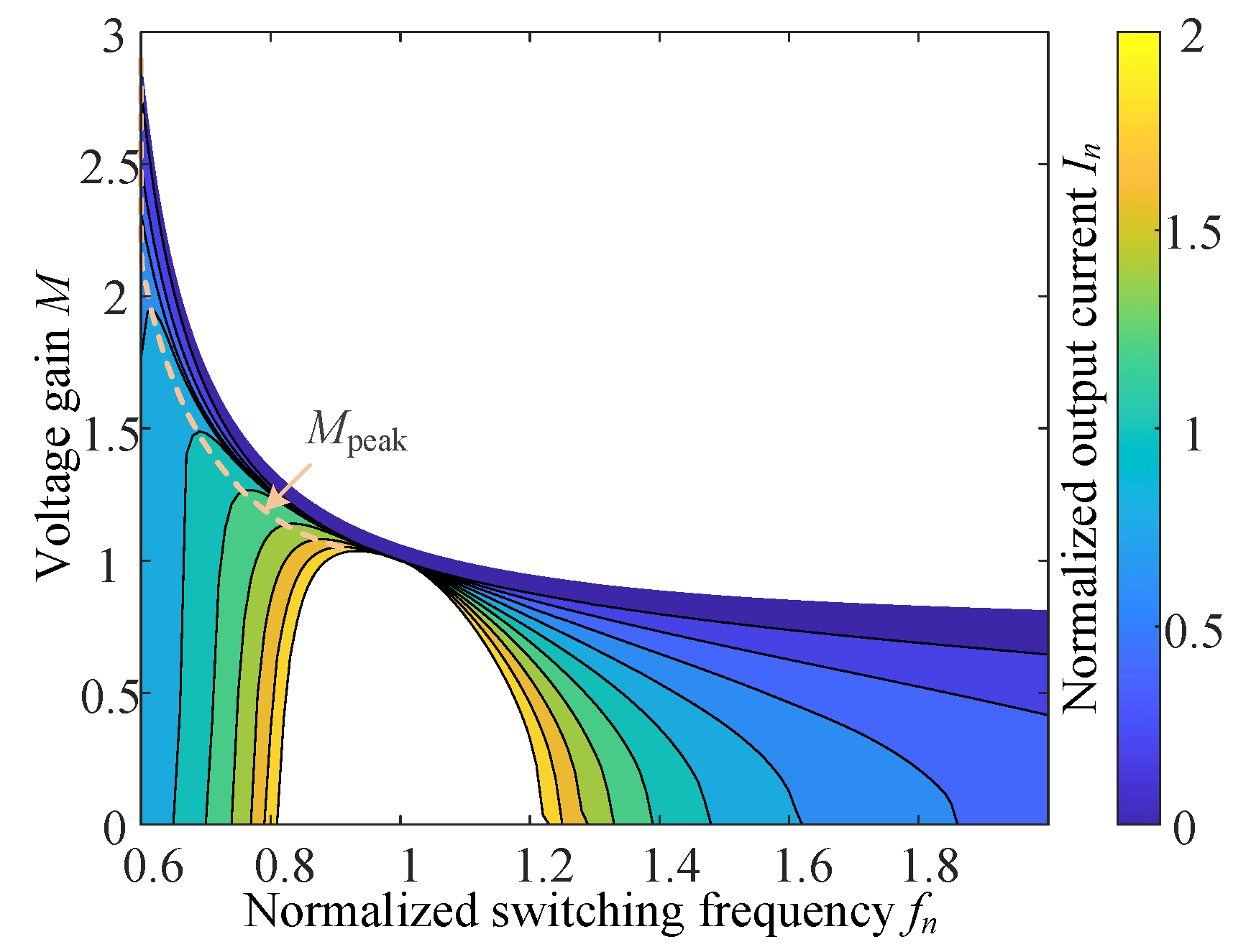
Figure 5.
Contour projection of in the -M plane.
Figure 5.
Contour projection of in the -M plane.
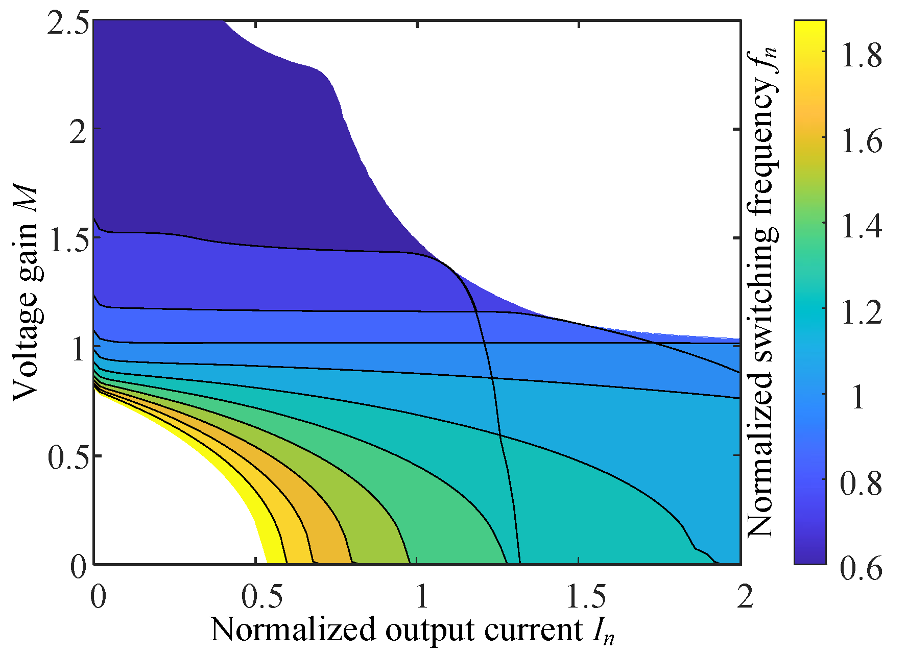
Figure 6.
Contour projection of in the -M plane.
Figure 6.
Contour projection of in the -M plane.
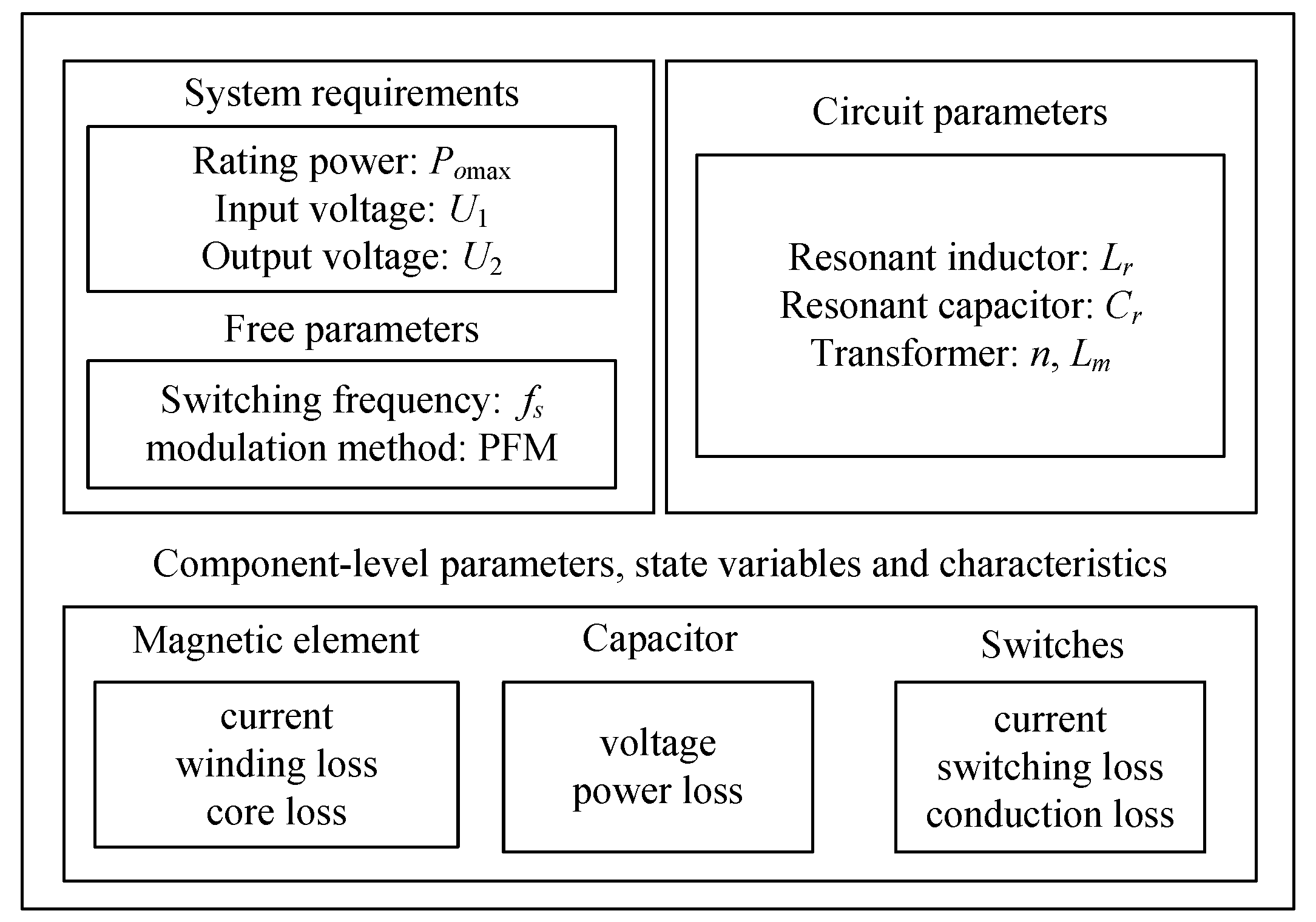
Figure 7.
Relationships among system requirements, circuit parameters, and state variables.
Figure 7.
Relationships among system requirements, circuit parameters, and state variables.
Figure 8.
Preliminary parameter design flowchart.
Figure 8.
Preliminary parameter design flowchart.
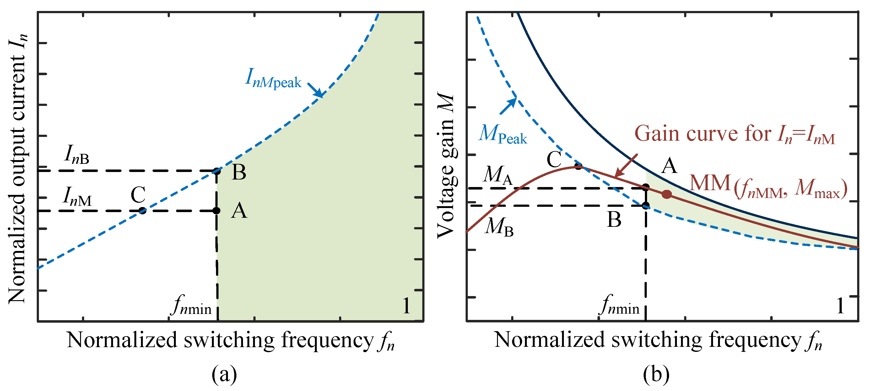
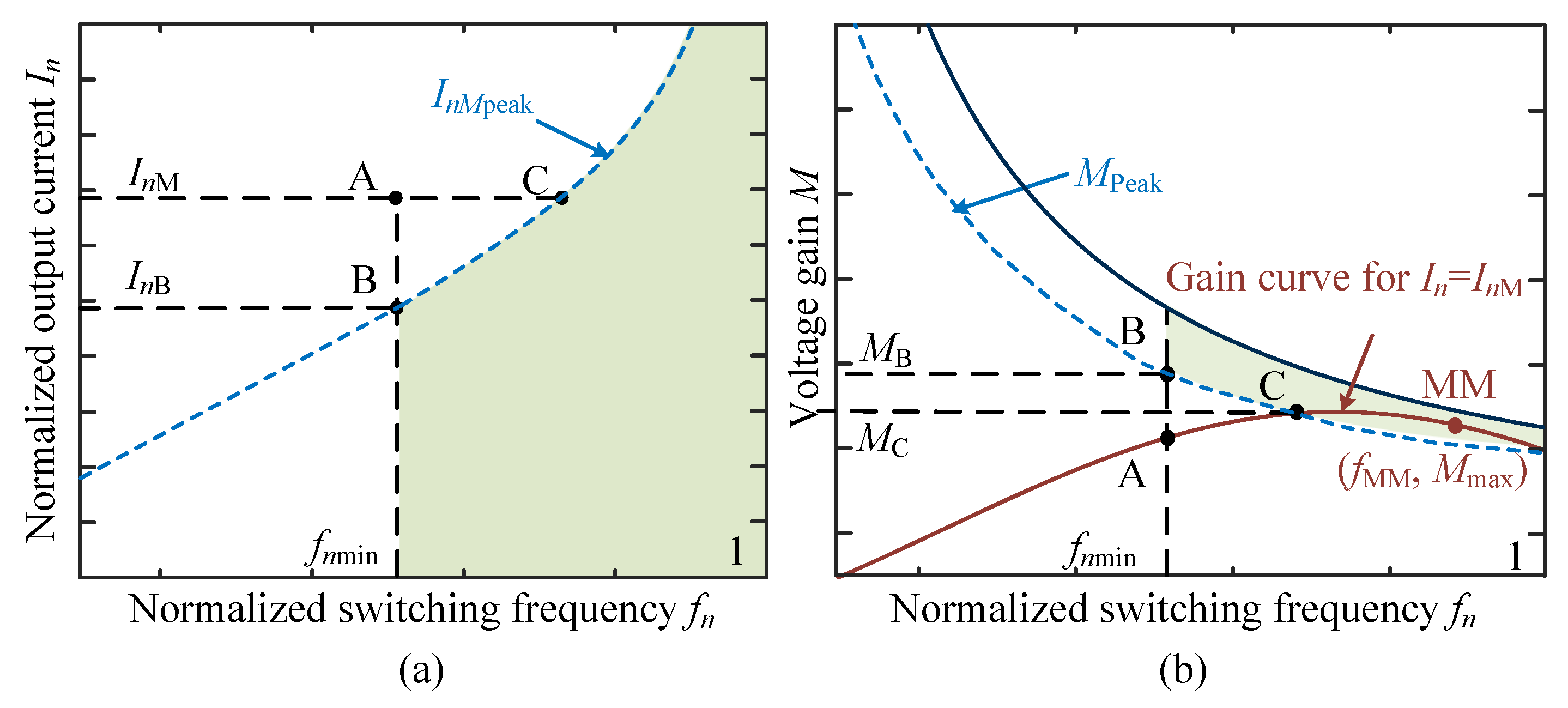
Figure 9.
Distribution of working points in - and -M for (a) -. (b) -M.
Figure 9.
Distribution of working points in - and -M for (a) -. (b) -M.
Figure 10.
Distribution of working points in - and -M for (a) -. (b) -M.
Figure 10.
Distribution of working points in - and -M for (a) -. (b) -M.
Figure 11.
and surfaces for voltage gain at different and for n = 8.
Figure 11.
and surfaces for voltage gain at different and for n = 8.
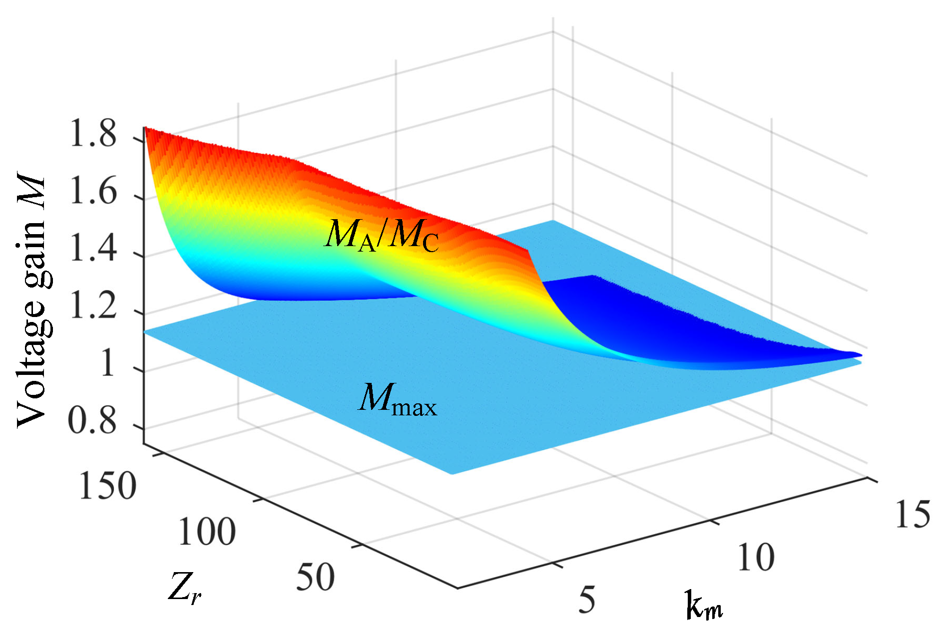
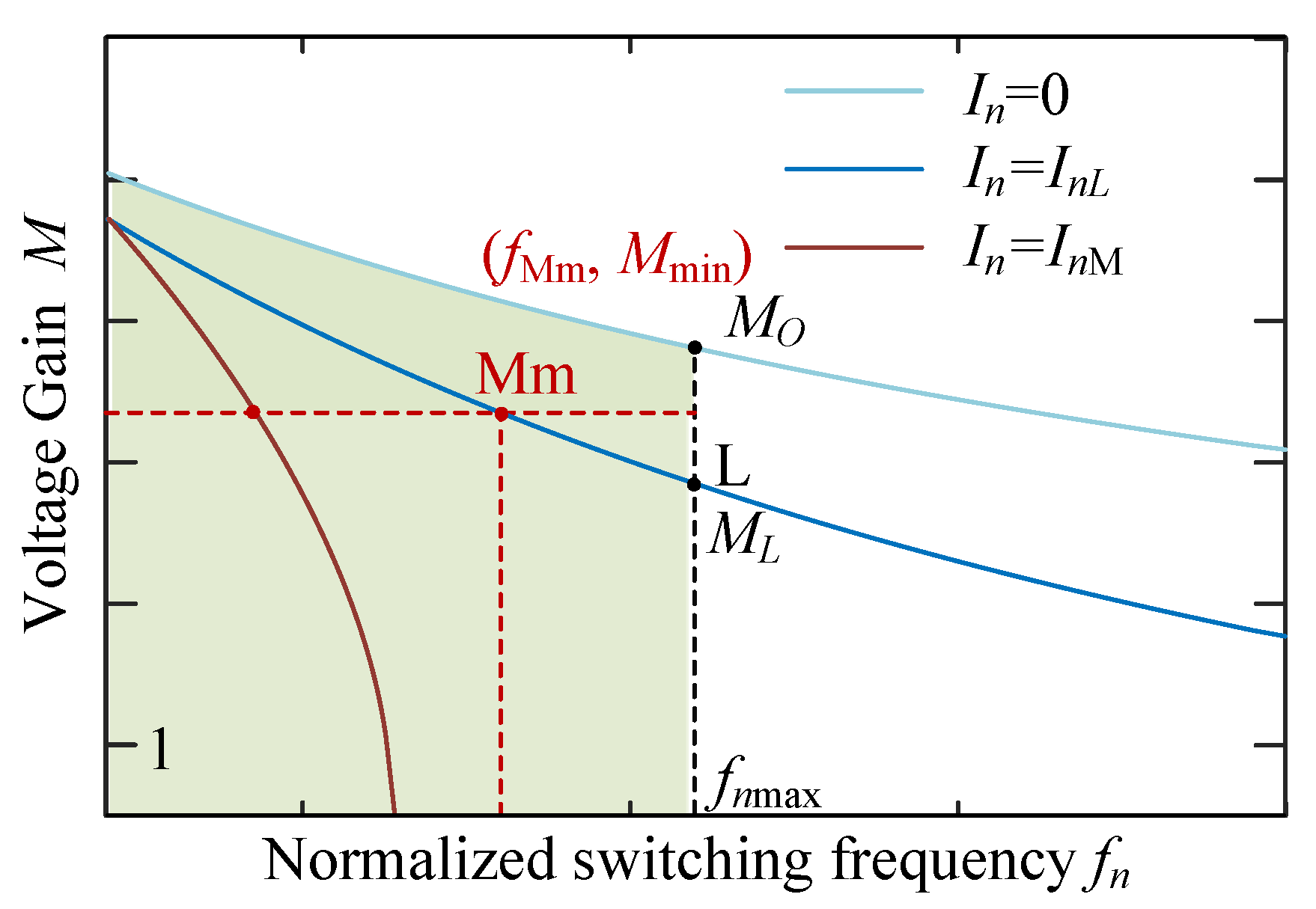
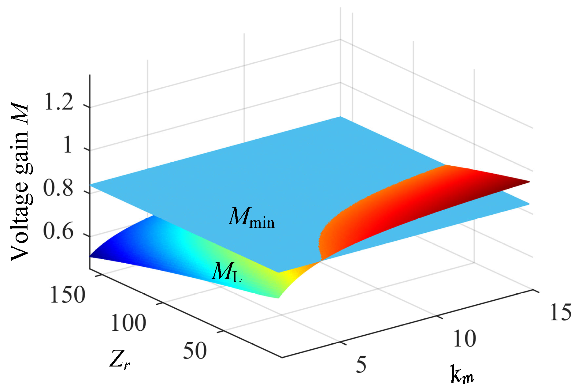
Figure 12.
Voltage gain curves at light load and no load in the ARR.
Figure 12.
Voltage gain curves at light load and no load in the ARR.
Figure 13.
Surfaces corresponding to voltage gains and for different and for .
Figure 13.
Surfaces corresponding to voltage gains and for different and for .
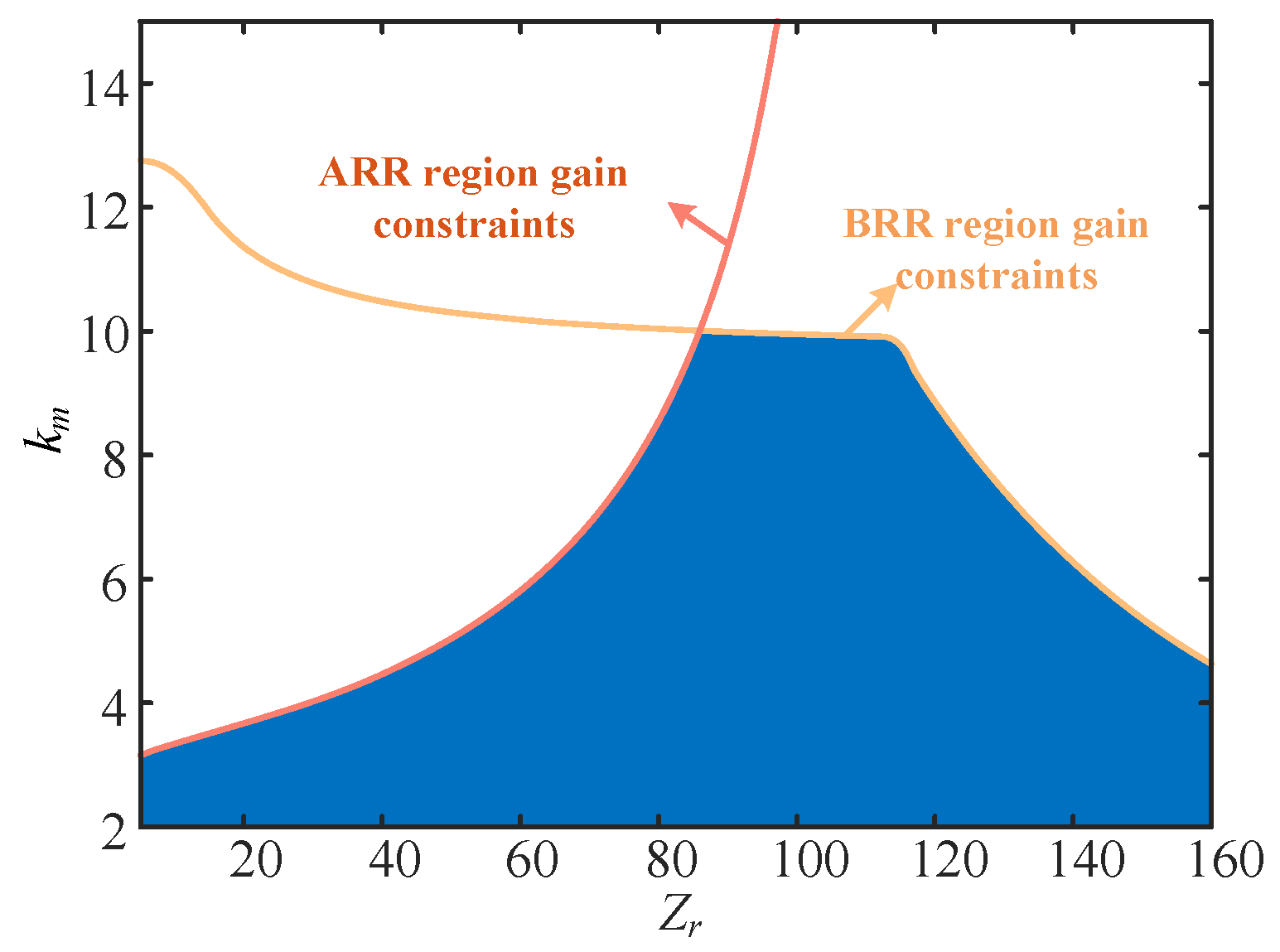
Figure 14.
- preliminary parameter constraint space when .
Figure 14.
- preliminary parameter constraint space when .
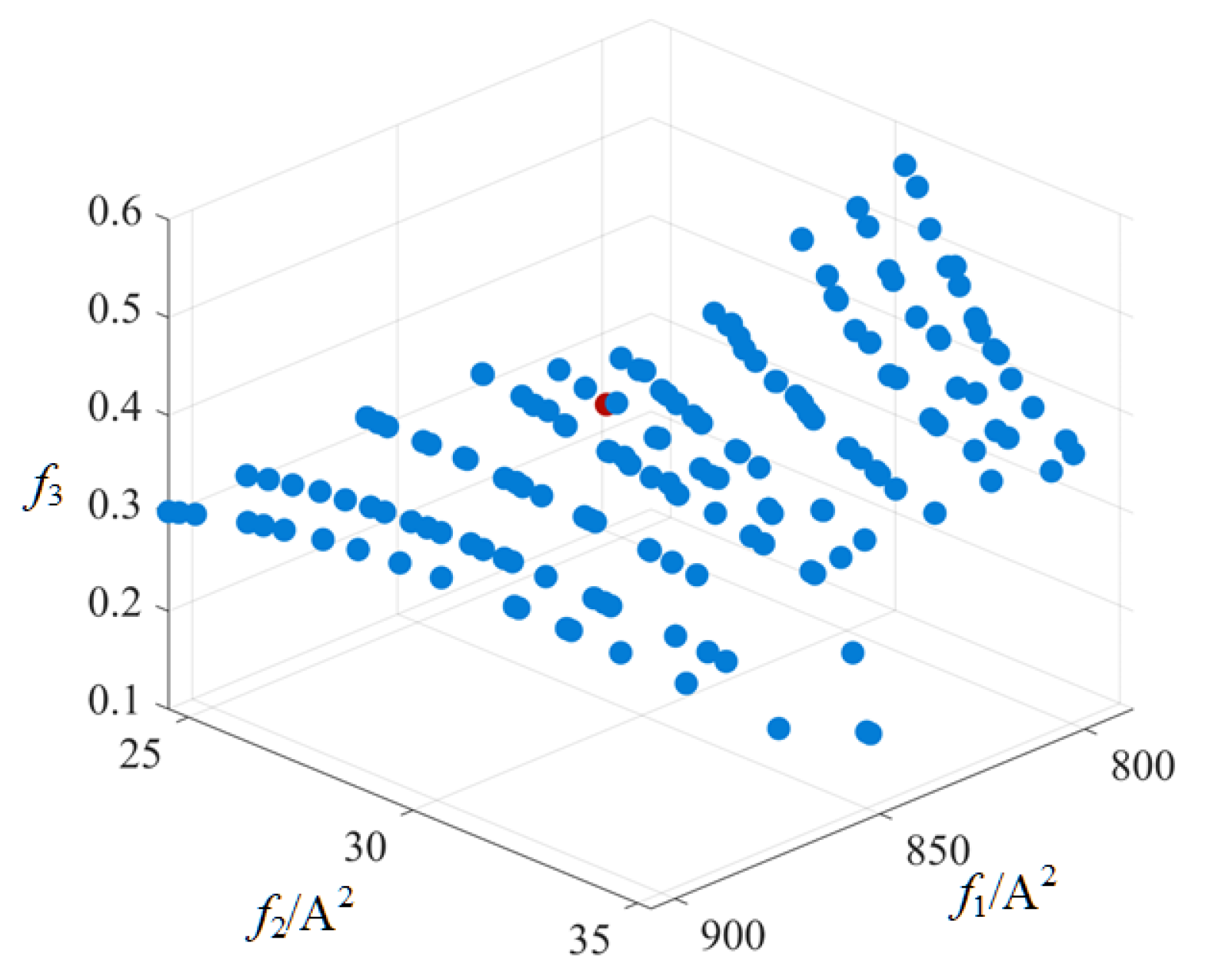
Figure 15.
The Optimal set of objective functions obtained by ANSGA-III.
Figure 15.
The Optimal set of objective functions obtained by ANSGA-III.
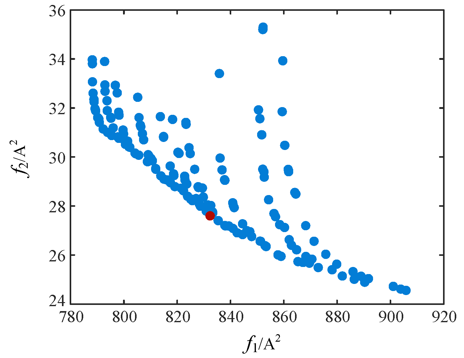
Figure 16.
The optimal set of objective functions in the - plane.
Figure 16.
The optimal set of objective functions in the - plane.
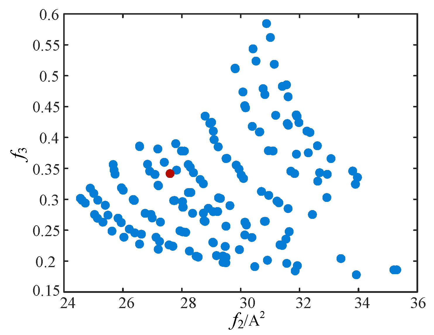
Figure 17.
The optimal set of objective functions in the - plane.
Figure 17.
The optimal set of objective functions in the - plane.
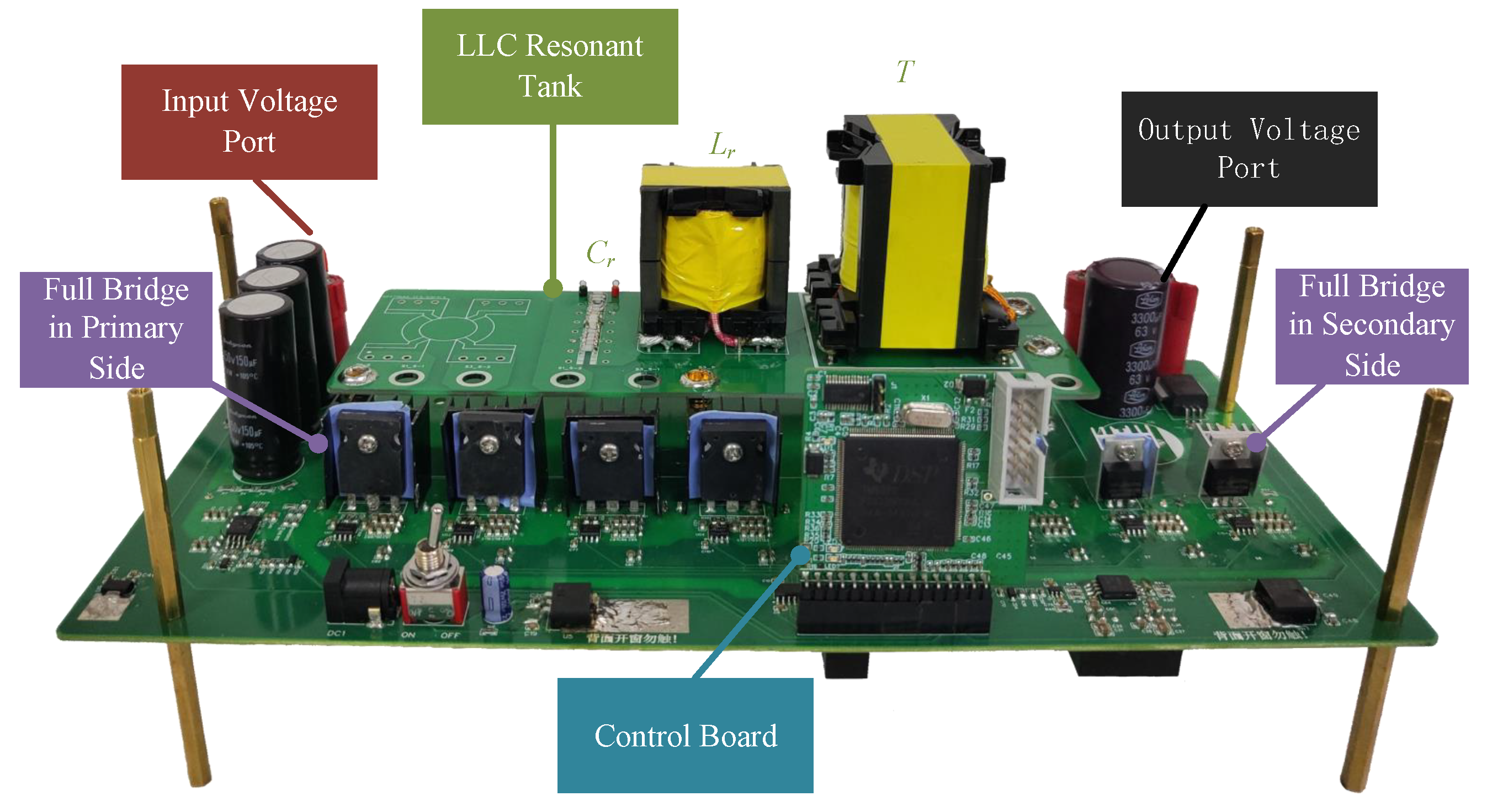
Figure 18.
Experimental prototype of LLC resonant converter.
Figure 18.
Experimental prototype of LLC resonant converter.
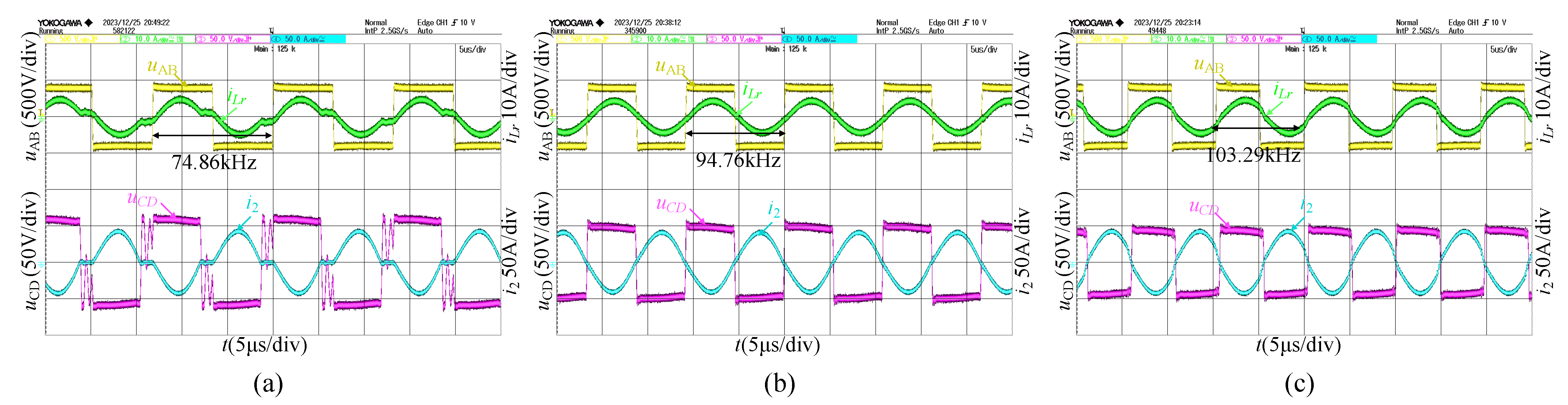
Figure 19.
Key waveforms of the LLC prototype under 1200 W load condition in forward mode. (a) V, V, . (b) V, V, . (c) V, V, .
Figure 19.
Key waveforms of the LLC prototype under 1200 W load condition in forward mode. (a) V, V, . (b) V, V, . (c) V, V, .
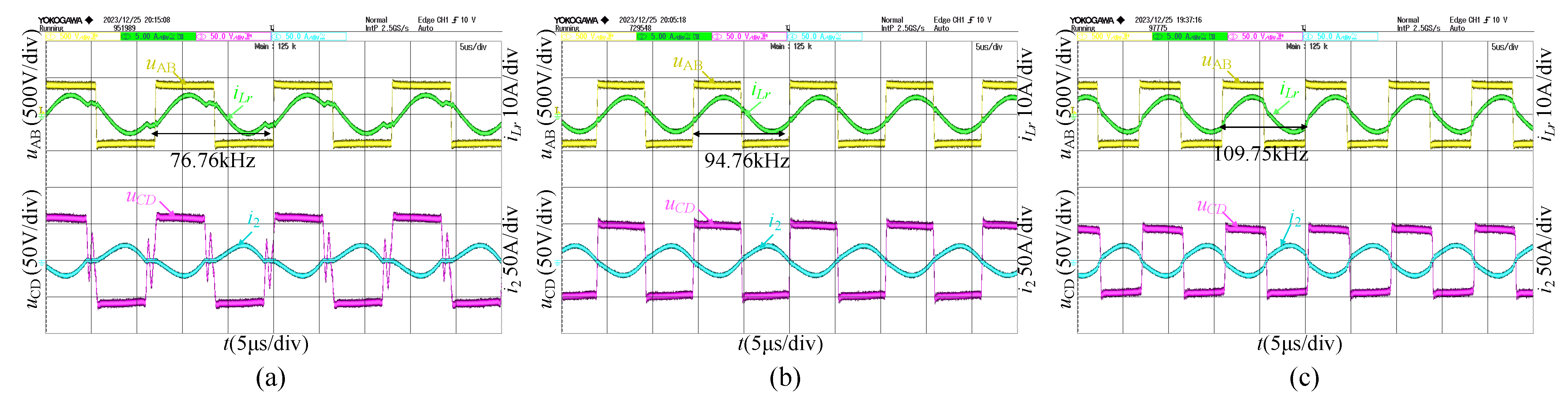
Figure 20.
Key waveforms of the LLC prototype under 600 W load condition in forward mode. (a) V, V, . (b) V, V, . (c) V, V, .
Figure 20.
Key waveforms of the LLC prototype under 600 W load condition in forward mode. (a) V, V, . (b) V, V, . (c) V, V, .
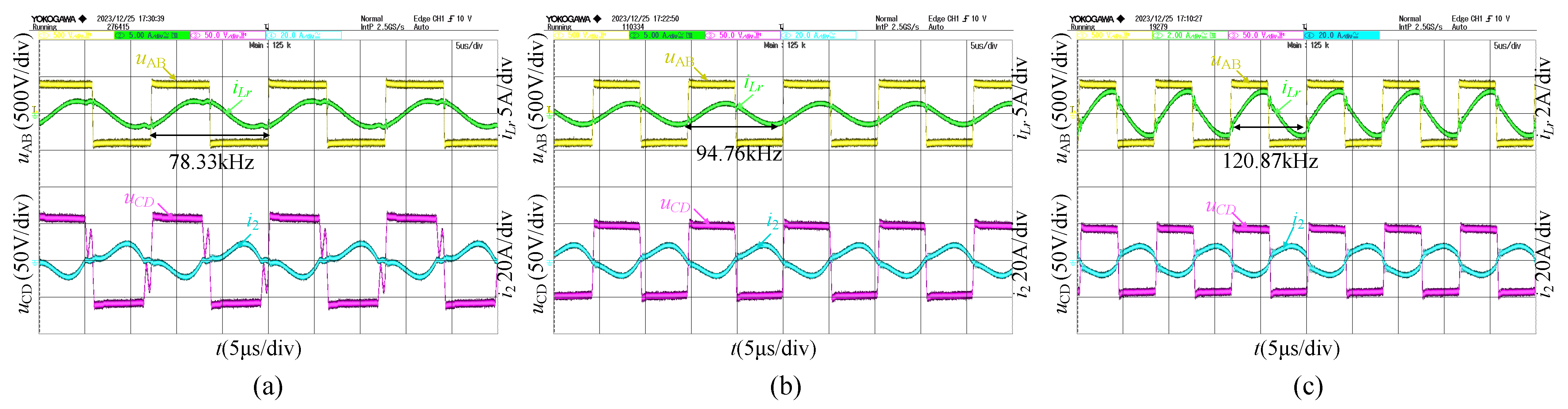
Figure 21.
Key waveforms of the LLC prototype under 240 W load condition in forward mode. (a) V, V, . (b) V, V, . (c) V, V, .
Figure 21.
Key waveforms of the LLC prototype under 240 W load condition in forward mode. (a) V, V, . (b) V, V, . (c) V, V, .
Figure 22.
Key waveforms of the LLC prototype under 1200 W load condition in forward mode. (a) V, V, V, V. (b) V, V, V, . (c) V, A, A, V.
Figure 22.
Key waveforms of the LLC prototype under 1200 W load condition in forward mode. (a) V, V, V, V. (b) V, V, V, . (c) V, A, A, V.
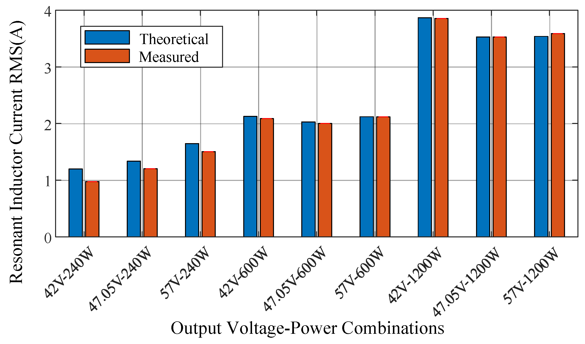
Figure 23.
Comparison of measured and theoretical RMS values of resonant inductor currents for different combinations of output voltage and power.
Figure 23.
Comparison of measured and theoretical RMS values of resonant inductor currents for different combinations of output voltage and power.
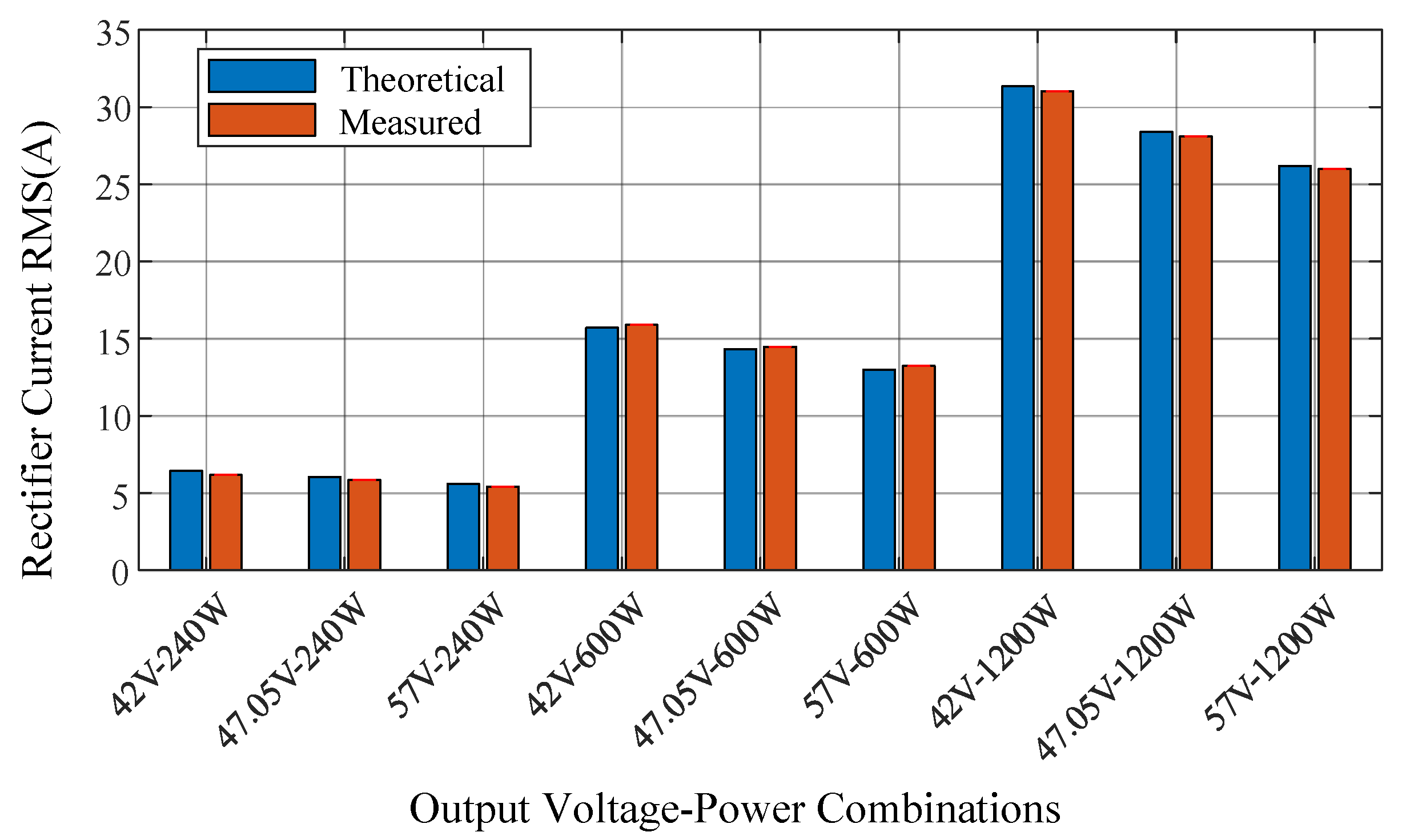
Figure 24.
Comparison of measured and theoretical RMS values of rectifier currents on the verside side for different output voltage and power combinations.
Figure 24.
Comparison of measured and theoretical RMS values of rectifier currents on the verside side for different output voltage and power combinations.
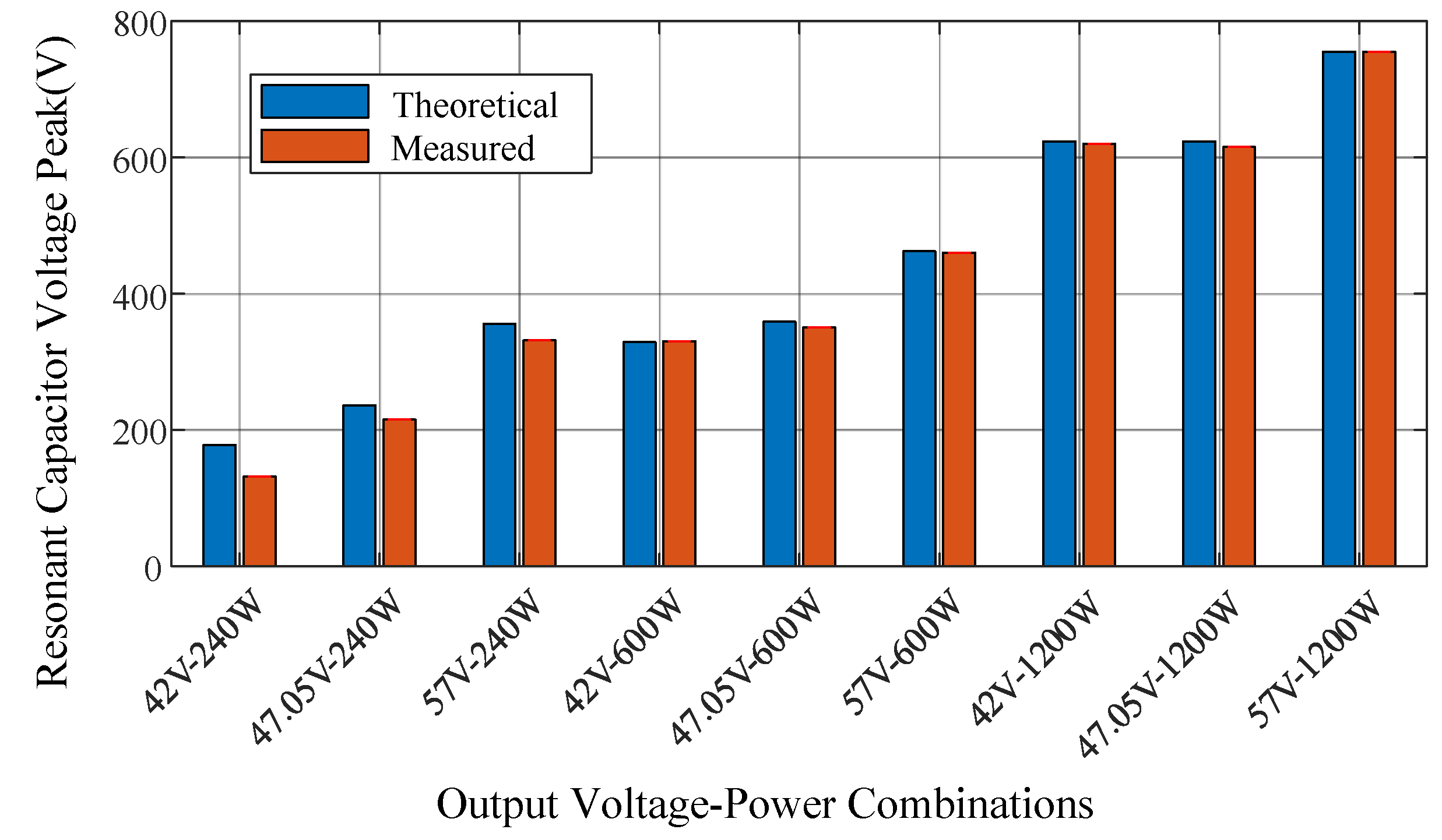
Figure 25.
Comparison of measured and theoretical peak values of resonant capacitor voltage for different combinations of output voltage and power.
Figure 25.
Comparison of measured and theoretical peak values of resonant capacitor voltage for different combinations of output voltage and power.
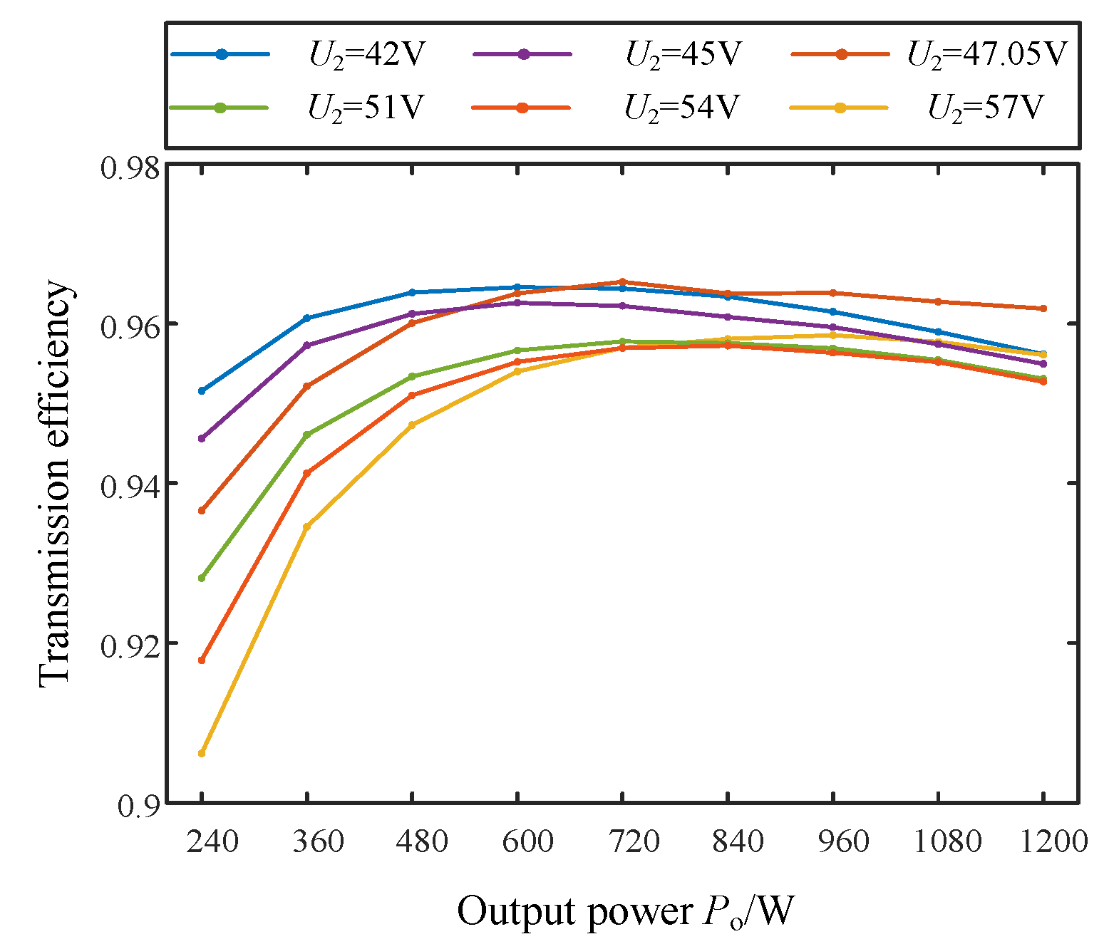
Figure 26.
Efficiency curves.
Figure 26.
Efficiency curves.
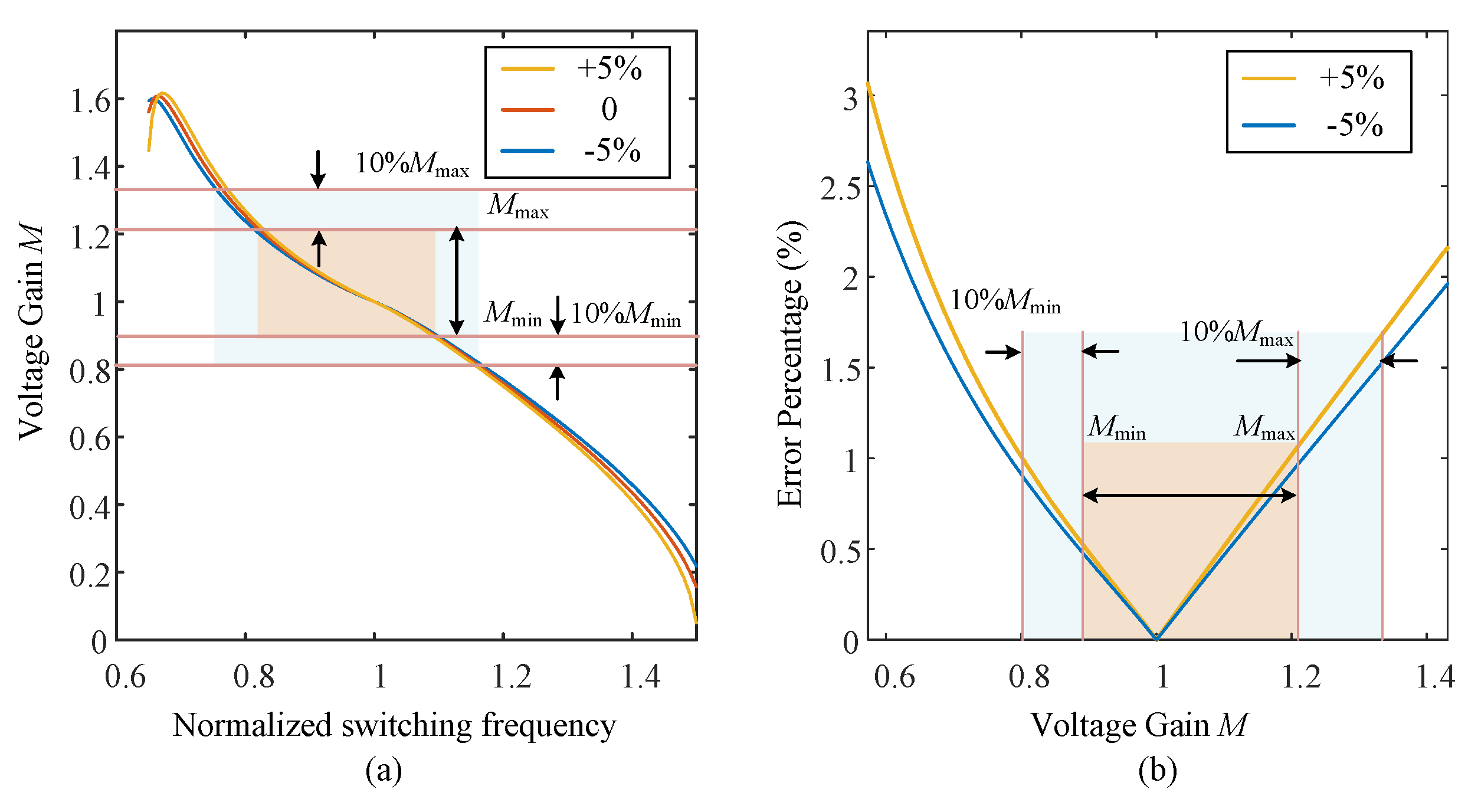
Figure 27.
Effect of circuit parameter tolerance on the gain curve. (a) Voltage gain curves at 5% tolerances. (b) Variation in voltage gain error percentage with voltage gain at 5% tolerance.
Figure 27.
Effect of circuit parameter tolerance on the gain curve. (a) Voltage gain curves at 5% tolerances. (b) Variation in voltage gain error percentage with voltage gain at 5% tolerance.
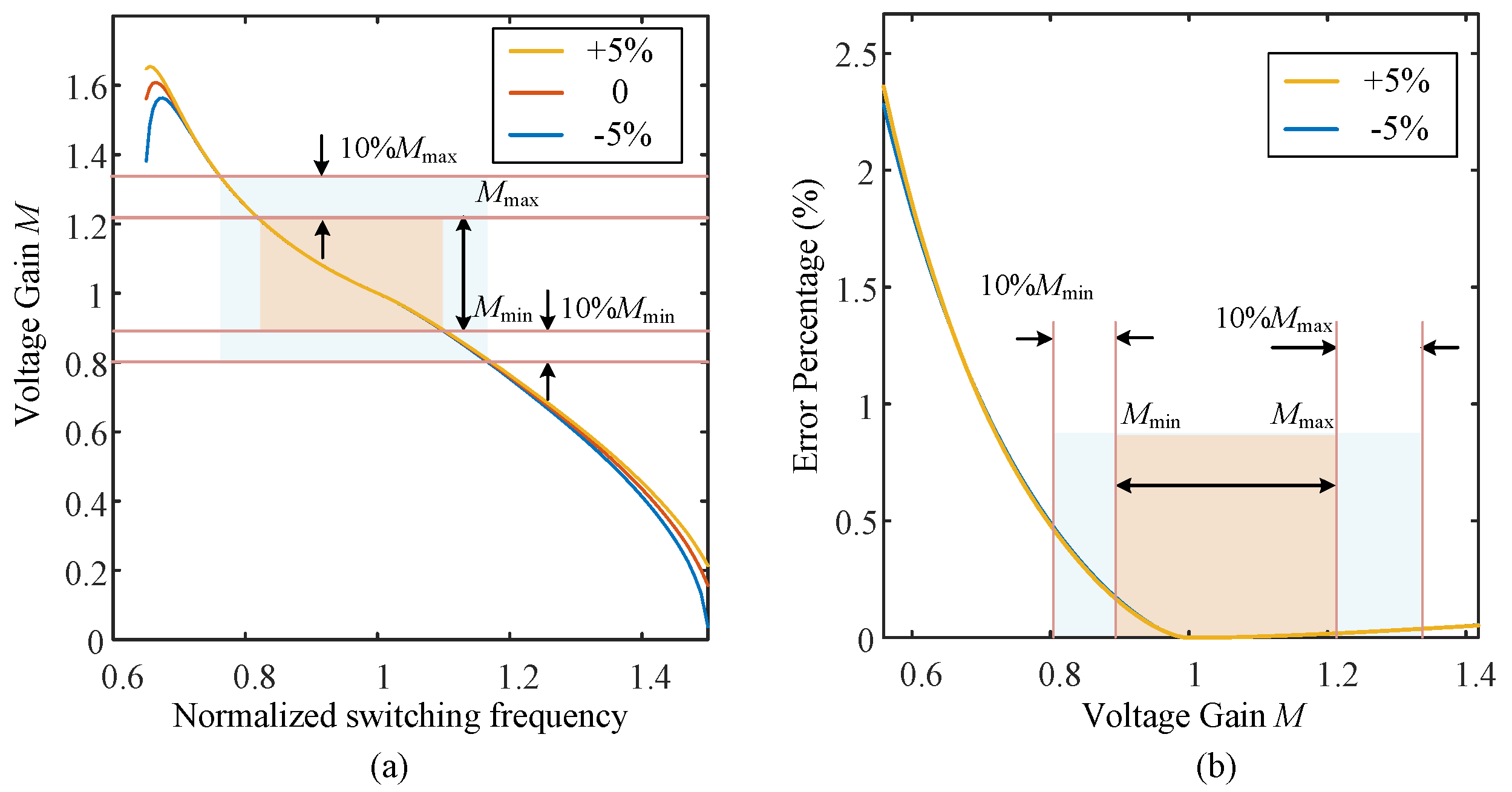
Figure 28.
Effect of circuit parameter tolerance on the gain curve. (a) Voltage gain curves at 5% tolerances. (b) Variation in voltage gain error percentage with voltage gain at 5% tolerance.
Figure 28.
Effect of circuit parameter tolerance on the gain curve. (a) Voltage gain curves at 5% tolerances. (b) Variation in voltage gain error percentage with voltage gain at 5% tolerance.
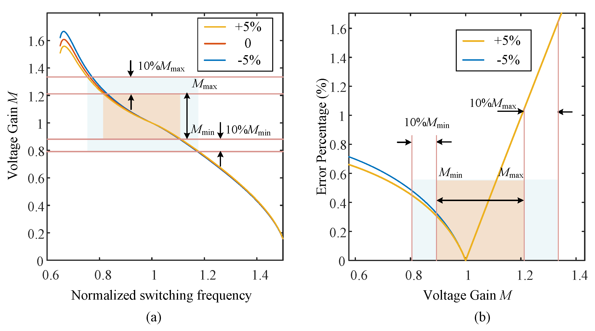
Figure 29.
Effect of circuit parameter tolerance on the gain curve. (a) Voltage gain curves at 5% tolerances. (b) Variation in voltage gain error percentage with voltage gain at 5% tolerance.
Figure 29.
Effect of circuit parameter tolerance on the gain curve. (a) Voltage gain curves at 5% tolerances. (b) Variation in voltage gain error percentage with voltage gain at 5% tolerance.
Table 1.
Comparisons among different design methods.
Table 1.
Comparisons among different design methods.
| Methods | Analysis Model | Voltage Gain | Consideration | Optimization Objective | Operating Mode |
|---|
| [6,7,8,12] | TDM | Wide range | Voltage gain | - | Peak voltage gain |
| [9] | TDM | Unity | - | Loss models | - |
| [10] | FHA+TDM | Wide range | ZVS, voltage gain | - | Depending on the battery characteristics |
| [11] | TDM | Wide range | ZVS, voltage gain | TWAE | Depending on the battery characteristics |
| [13] | TDM | Wide range | ZVS, voltage gain | Loss models | - |
| [1] | TDM | Wide range | ZVS, voltage gain, , | Loss models | PO mode |
| [15] | TDM | Wide range | ZVS, voltage gain, , | | - |
| [14] | data-driven surrogate model | Wide range | ZVS, voltage gain, | , , | PO mode |
| [16] | TDM | Nearby unity | ZVS, parasitic capacitance | Loss models | - |
| Proposed | TDM | Wide range | ZVS, voltage gain, | , , Switching frequency range | Voltage gain monotonic region |
Table 2.
Variables and normalization.
Table 2.
Variables and normalization.
| Circuit Variable | Symbol | Normalized Variable |
|---|
| Resonant frequency | | - |
| Characteristic impedance | | - |
| Excitation inductance ratio | = | - |
| Voltage gain | | - |
| Switching frequency | | |
| Time | t | |
| Reflected output current | | |
| Reflected output voltage | | |
| Transmission power | | |
Table 3.
Parameter design requirements.
Table 3.
Parameter design requirements.
| System Requirements | Range |
|---|
| Input voltage | 400 V (DC) |
| Output voltage | 42–57 V (DC) |
| Switching frequency | 60–200 kHz |
| Rated power | 1200 W |
Table 4.
Key operating situations for forward mode in the BRR.
Table 4.
Key operating situations for forward mode in the BRR.
| Operating Situations | Known Condition | Results of the Time-Domain Model Solution |
|---|
| A | , | |
| B | | |
| C | | |
| MM | , | |
Table 5.
Key operating situations for forward mode in the BRR.
Table 5.
Key operating situations for forward mode in the BRR.
| Operating Situations | Known Condition | Results of the Time-Domain Model Solution |
|---|
| L | , | |
| Mm | , | |
Table 6.
Key components and performance characterization parameters.
Table 6.
Key components and performance characterization parameters.
| Components | Performance Characterization | Key Variables |
|---|
| winding losses and core losses | , |
| T | winding losses and core losses | , , |
| losses and maximum voltage stress | , |
| Primary side switches | conduction loss | |
| Secondary side switches | conduction loss | |
Table 7.
Key components and performance characterization parameters.
Table 7.
Key components and performance characterization parameters.
| Components | Parameter/Part# |
|---|
| Turns ratio n | 8.5 |
| Excitation inductor | |
| Resonant inductor | |
| Resonant capacitor | |
| Resonant frequency | kHz
|
| Theoretical switching frequency | 78.35–110.05 kHz |
| Transformer cores | PQ5050 PC95 |
| Inductive cores | PQ3535 PC95 |
| Primary side switches | ROHM SCT3060AR |
| Secondary side switches | CRMICRO CRST045N10N |


