Abstract
In the context of increasing digitalization and the emergence of applications such as smart cities, embedded devices are becoming ever more pervasive, mobile, and ubiquitous. Due to increasing concerns around energy efficiency, gate density, and scalability in the semiconductor industry, there has been much interest recently in the fabrication of viable low-power energy-efficient devices. The Hetero-Dielectric Gate-All-Around (HD-GAA) MOSFET represents a cutting-edge transistor architecture designed for superior sustainability and energy efficiency, improving the overall efficiency of the system by reducing leakage and enhancing gate control; therefore, as part of the transition to a sustainable future, several semiconductor industries, including Intel, Samsung, Texas Instruments, and IBM, are using this technology. In this study, Hetero-Dielectric Single-Metal Gate-All-Around MOSFET (HD-SM-GAA MOSFET) devices and circuits were designed using Schottky source/drain contacts and tunable high-k dielectric HfxTi1−xO2 in the TCAD simulator using the following specifications: N-Channel HD-SM-GAA MOSFET (‘Device-I’) with a 5 nm radius and a 21 nm channel length alongside two P-Channel HD-SM-GAA MOSFETs (‘Device-II’ and ‘Device-III’) with radii of 5 nm and 8 nm, respectively, maintaining the same channel length. Thereafter, the inverters were implemented using these devices in the COGENDA TCAD simulator. The results demonstrated significant reductions in short-channel effects: subthreshold swing (SS) (‘Device-I’ = 61.5 mV/dec, ‘Device-II’ = 61.8 mV/dec) and drain-induced barrier lowering (DIBL) (‘Device-I’ = 8.2 mV/V, ‘Device-II’ = 8.0 mV/V) in comparison to the existing literature. Furthermore, the optimized inverters demonstrated significant improvements in noise margin values such as Noise Margin High (NMH) and Noise Margin Low (NML), with Inverter-1 showing 38% and 44% enhancements and Inverter-2 showing 40% and 37% enhancements, respectively, compared to the existing literature. The results achieved illustrate the potential of using this technology (e.g., for power inverters) in embedded power control applications where energy efficiency and scalability are important, such as sustainable smart cities.
1. Introduction
The increasing digitalization and penetration of intelligent embedded power control devices in applications such as smart grids and smart cities drive a growing need for sustainable, energy-efficient, and reliable electronics. This, in turn, has fueled research and transistor technology development. Transistors, the foundation of contemporary electronics, must provide exceptional switching performance coupled with low-parasitic power or signal losses, ideally with a size/density and manufacturing footprint that is favorable in terms of economic costs and harm to the environment [1,2,3]. The energy efficiency, scalability, and leakage control of conventional planar and Fin Field-Effect Transistor (FinFET) designs are constrained, especially in advanced technological nodes (sub-5 nm). Many innovative technologies have been invented and created over the past decades to enhance the functionality of devices and alleviate short-channel effects (SCEs), including strained silicon, high-metal gates, and three-dimensional (3D) device architectures [4,5,6,7]. The advancement of 3D designs and multiple gate field-effect transistors, such as multifaceted gate, Omega, Fin, and GAA FETs, demonstrates their supremacy beyond planner devices with aggressive complementary metal-oxide semiconductor (CMOS) scaling. Despite the higher process complexity and cost, GAA FETs offer better performance, lower leakage, and improved scalability, making them a necessary evolution beyond FinFETs. Over time, as fabrication techniques mature, costs may reduce, making GAAFETs more economically viable for large-scale production. Although more complex and costly at this stage compared to conventional FETs, cost and complexity are expected to reduce considerably due to miniaturization. Since FinFETs provide better electrostatic control of the channel than planar MOSFETs, they are the favored device design for the mass manufacturing of electronic components beyond the 32 nm technology node [8].
However, the performance, layout, and cost of FinFETs are now quite problematic, making future scaling of the transistors a tedious operation necessitating unique architectural designs. This is a barrier to their application in smart cities, where size/density, energy footprint, and development times and costs are critical. Without a doubt, among the many device structures employed, the ultimate scaled transistor structure GAA has shown promise for designing nano-scale devices because it provides electrostatic controllability by completely controlling the channel’s carriers via the gate with immunity to short channel effects and high current drivability, providing higher chip-packing density because of the perfectly circular configuration, negligible corner effects, huge transconductance, and a desirable sub-threshold slope [9,10,11]. Shorter channel lengths produce faster operating speeds and more components per chip [12]. A noteworthy property of GAA transistors is that their speed improves, and their cost drops as their size shrinks, driving the rapid expansion of the electronic technology sector [13]. According to IBM, a 150 mm2 device with a compact architecture employing GAAFET 2 nm technology may fit 50 billion transistors [14]. Due to the improved channel transport control provided entirely by the surrounding gates in GAAFETs, FinFETs are likely to be phased out in future technological nodes. In order to continue logical growth beyond the 5 nm technology node and beyond FinFETs, the industry has widely embraced GAAFETs, a novel next-generation transistor device [15]. The exceptional gate control and decrease in SCEs have also greatly improved the performance of analog and radio frequency (RF) devices [16]. However, the main disadvantage of these massively scaled devices is elevated series resistance as a result of the origination of unanticipated source/drain intersections. These shortcomings have led to the replacement of doped source/drain regions with novel approaches like the Schottky barrier/contact source and drain, enabling a greater ON-current and enhanced transconductance. Moreover, not only do Schottky barrier metal-oxide semiconductors have drain and source divisions made of aluminum that are likely to find numerous applications in deep micron-sized devices, but they also offer advantages in terms of cultivation [11]. To enhance these devices’ capabilities, many engineering approaches, such as bandgap engineering with hetero-junction devices and gate and work function engineering, have been investigated in the literature work [17]. High-k gate dielectric material such as HfxTi1−xO2 with a permittivity value above 40 has been preferred for sub-22 nm multi-gate FinFET devices. It allows the controllability of electrostatics and creates an effective link between the gate and the channel, which helps to reduce leakage current and other problems like SCEs [9]. Major semiconductor companies, including Intel, IBM, Samsung, and TSMC, have started employing high-k gate oxide and metallic gate materials in the manufacture of transistors for scaled devices [18,19,20,21]. The key characteristics of high-k gate dielectric include a high-energy bandgap and thermal and chemical stability with silicon and high crystallization temperatures [22].
To extend previous work and explore further developments in this area, in this article, we consider both N-Channel and P-Channel Hetero-Dielectric Single-Metal Gate-All-Around MOSFETs with Schottky source/drain contact, which were created in combination with device specifications such a tunable high-k dielectric (k) of HfxTi1−xO2, a 5 nm radius, and a 21 nm channel length. The same structures were used to construct the CMOS inverter. The remainder of this article has been organized as follows: In Section 2, the device design structures and simulation methodology of N-Channel and P-Channel HD-SM-GAA MOSFETs with Schottky source/drain contact are discussed. The design and structural arrangement of an inverter utilizing an HD-SM-GAA MOSFET with a Schottky source/drain contact is described in Section 3. The performance analysis and comparison of proposed devices and circuits are given in Section 4. Following that, the conclusion and future scope are explained and exposited in Section 5.
2. Device Structure and Simulation Methodology
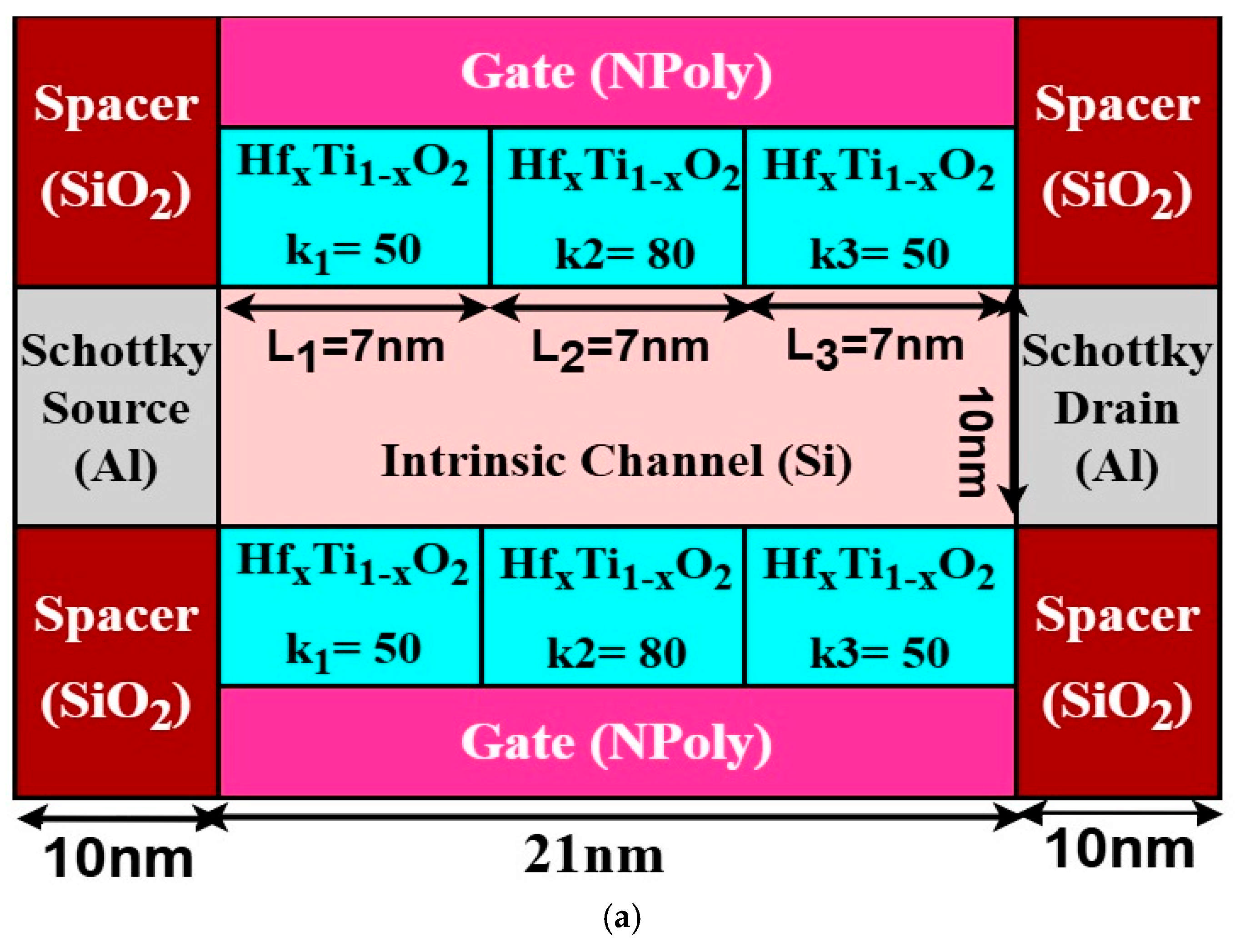
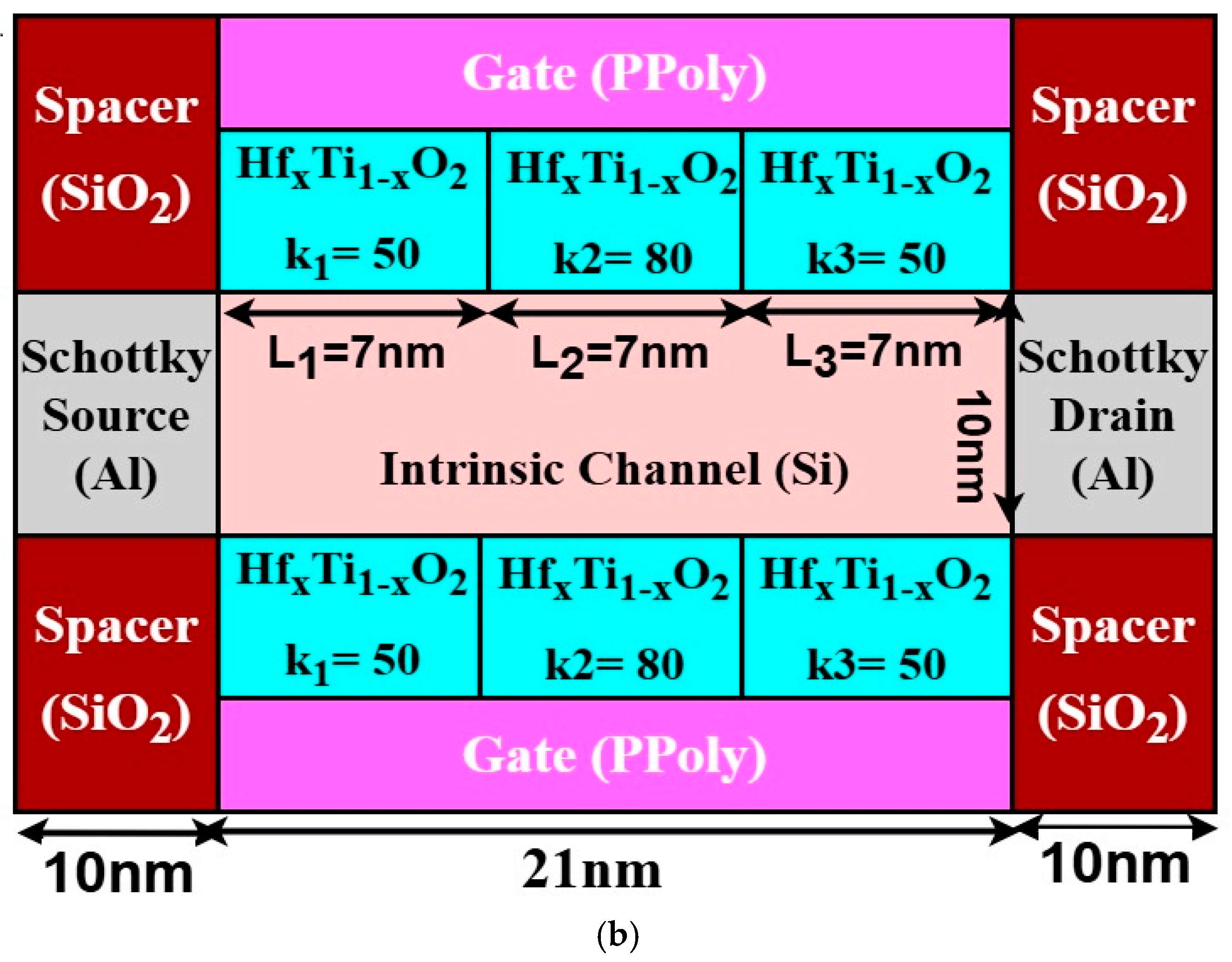
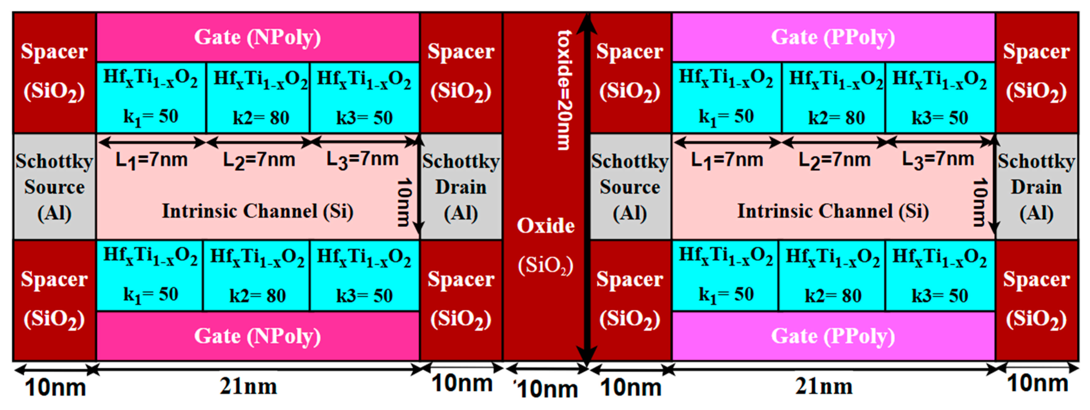
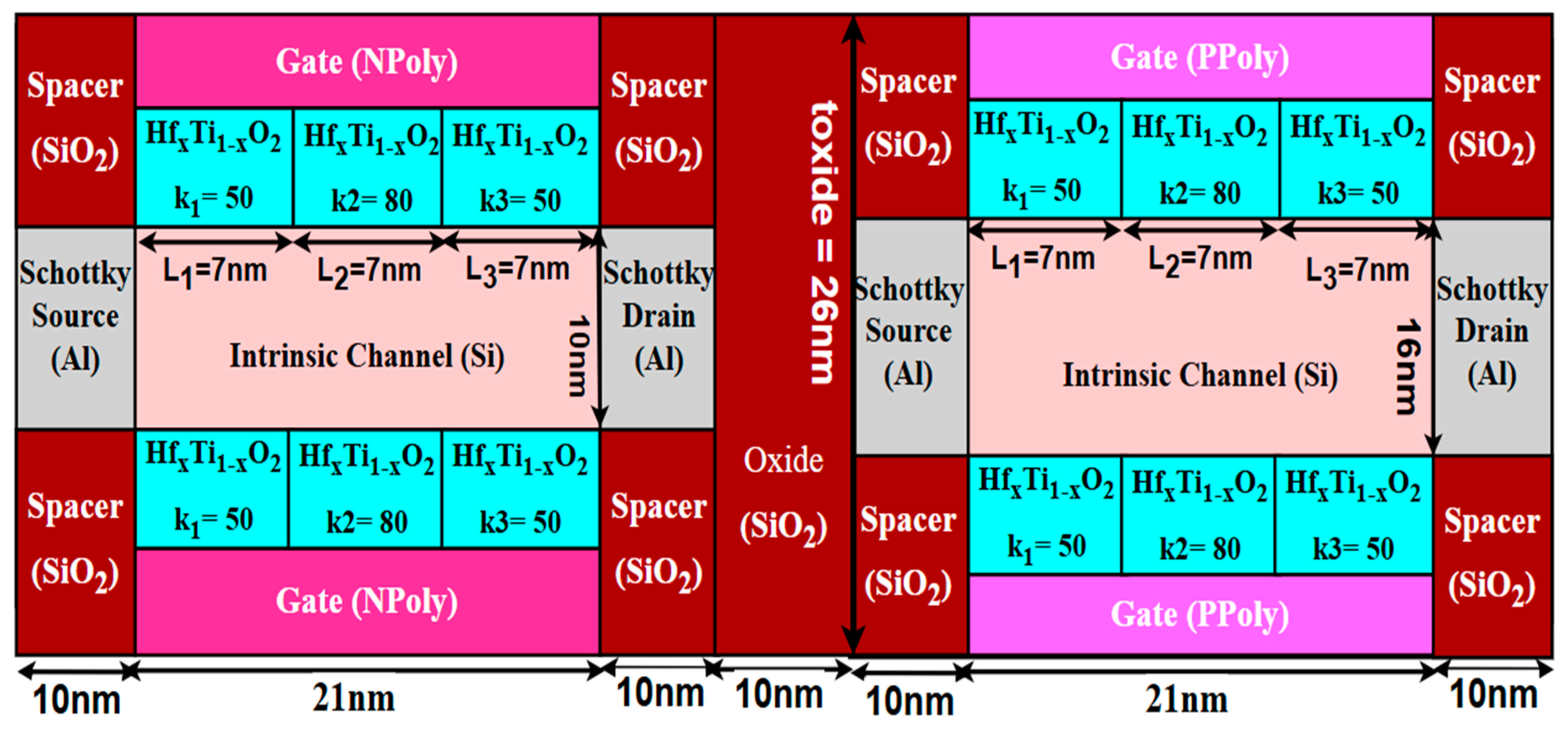
Using the COGENDA TCAD simulator, the following devices with a channel length of 21 nm were created: (1) ‘Device-I’, i.e., an N-Channel HD-SM-GAA MOSFET (radius 5 nm); (2) ‘Device-II’, i.e., a P-Channel HD-SM-GAA MOSFET of 5 nm radius; and (3) ‘Device-III’, i.e., a P-Channel HD-SM-GAA MOSFET of 8 nm radius. The design specifications used for the proposed structures are shown in Table 1. The design parameters of GAA transistors were selected according to Intel dimensions [23]. Figure 1 shows the 2D structures of the proposed devices (a) ‘Device-I’ and (b) ‘Device-II’ of 5 nm radius, 21 nm channel length (L1 = 7 nm + L2 = 7 nm + L3 = 7 nm), and tunable compound (high-k) gate dielectric HfxTi1−xO2 material (k1 = 50, k2 = 80, and k3 = 50). The amalgamation of two oxide materials (HfO2 and TiO2) was chosen to increase the permittivity value to greater than 50. The potential of an insulator is increased by a greater dielectric constant value. Chemical vapor deposition (CVD) is often used to deposit the chosen compound dielectric material, such as HfxTi1−xO2 film, on silicon at temperatures as high as 1000 °C. Unwavering coverage over intricate layouts and fast, flexible growth rates are two benefits of the CVD process [24]. Leakage current and static power consumption are greatly reduced using the high-k gate dielectric because it increases gate capacitance in the structure [22]. Schottky source/drain regions made with aluminum metal and spacer regions and developed with silicon dioxide (SiO2) provide low parasitic effects in proposed devices [25,26].

Table 1.
Design description of proposed structures (‘Device-I’, ‘Device-II’ and ‘Device-III’).
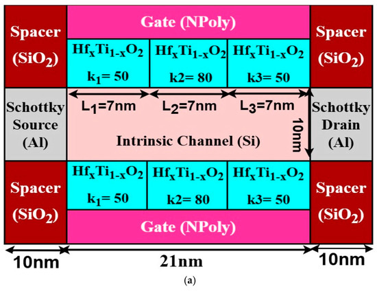
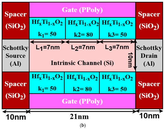
Figure 1.
Two-dimensional structures of (a) ‘Device-I’ and (b) ‘Device-II’ for k1 = 50, k2 = 80, and k3 = 50.
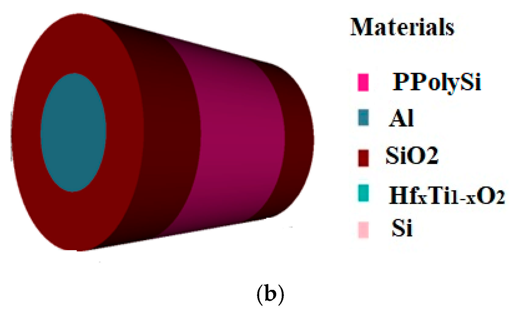
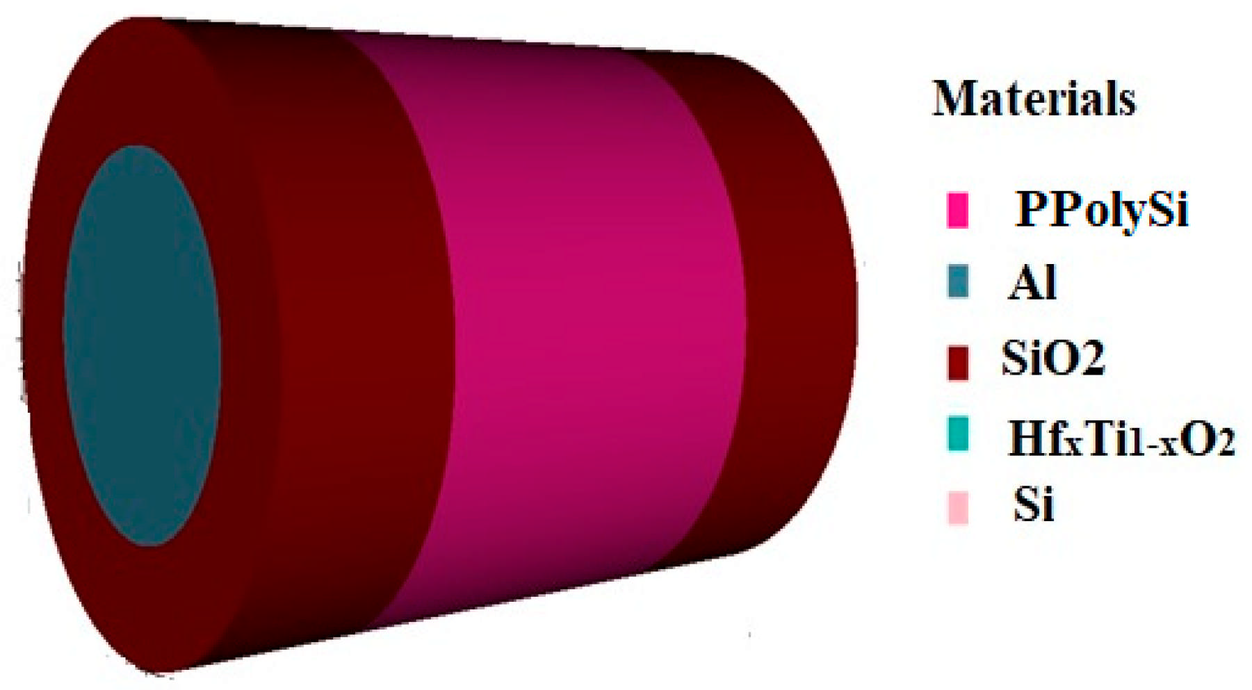
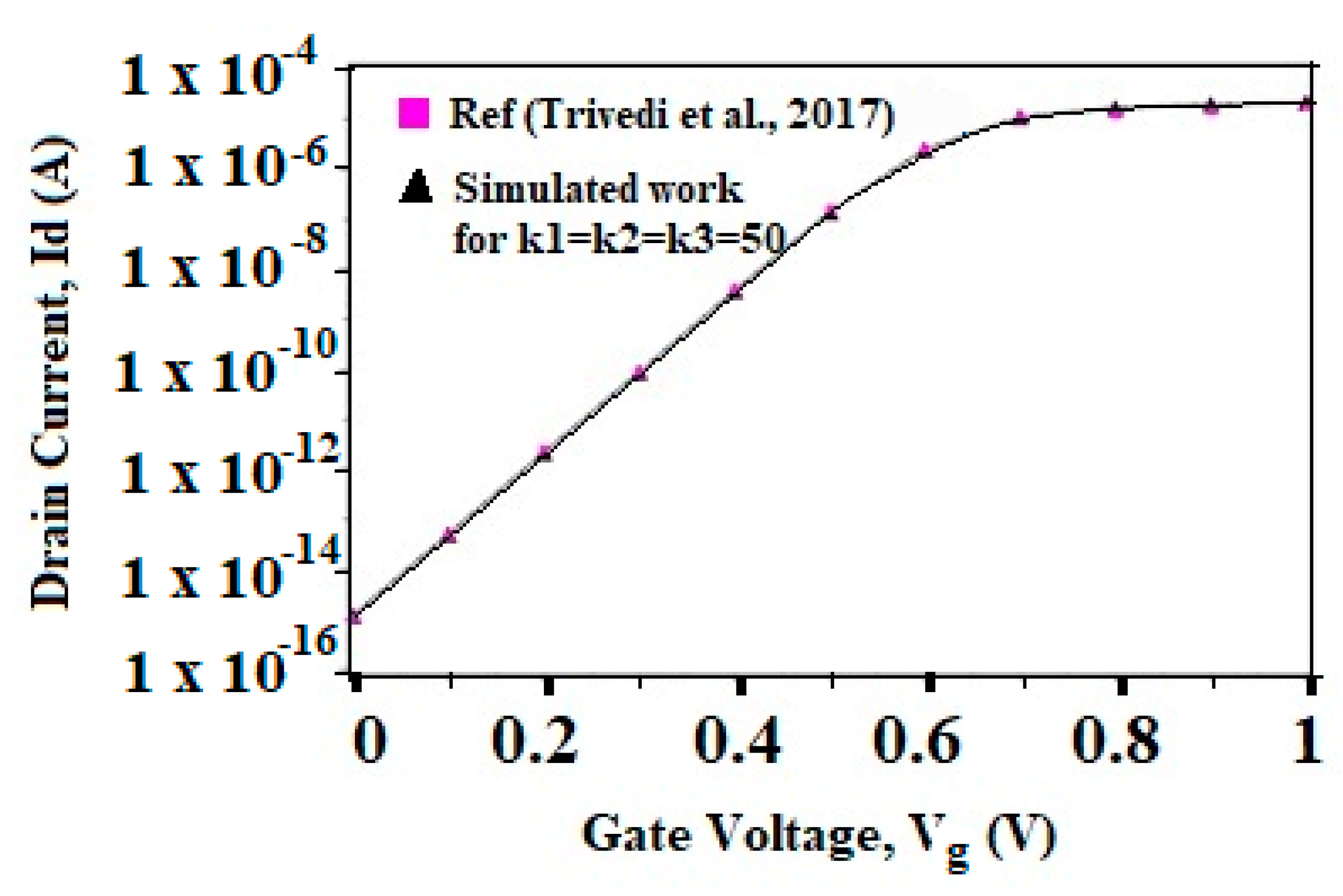
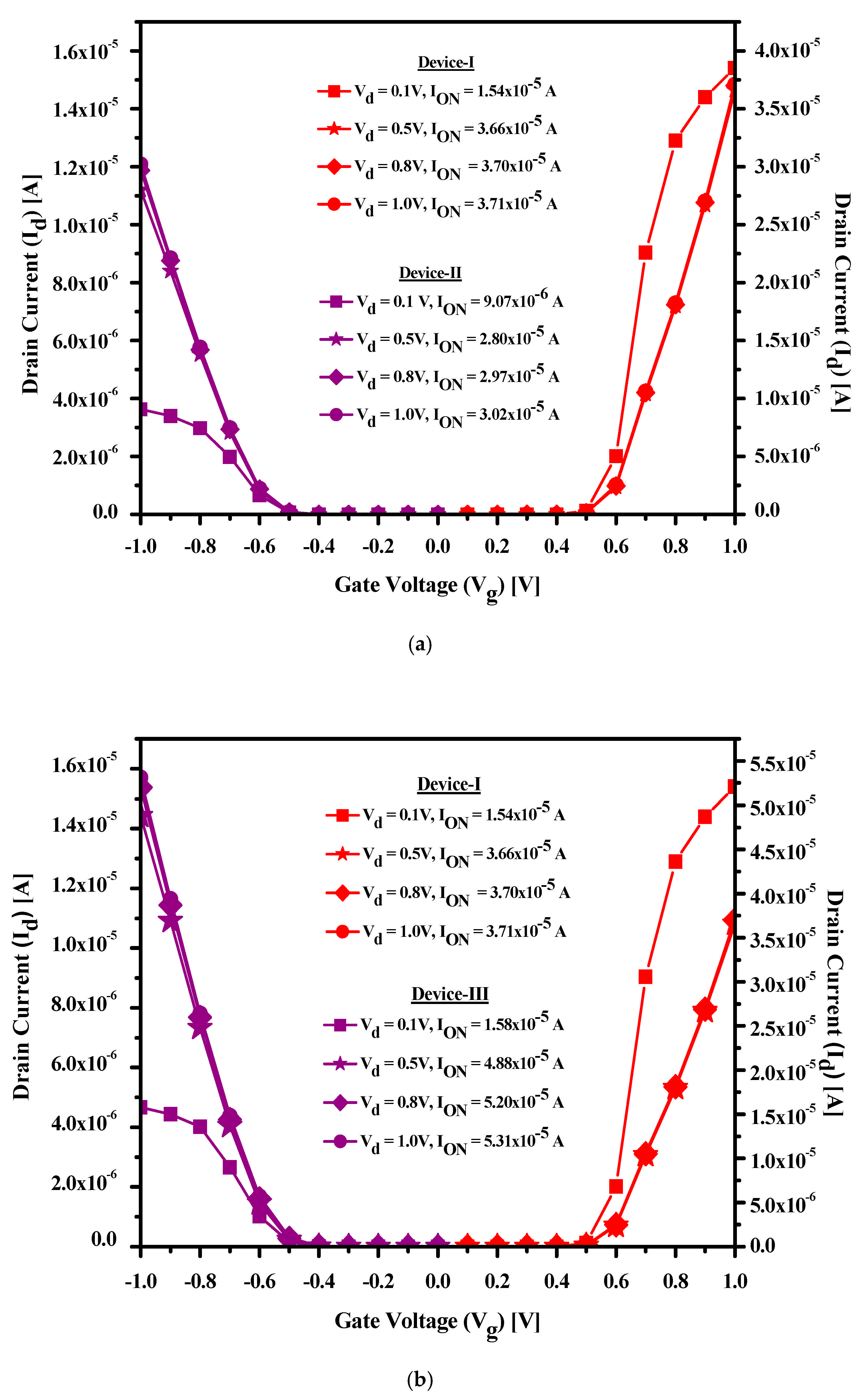
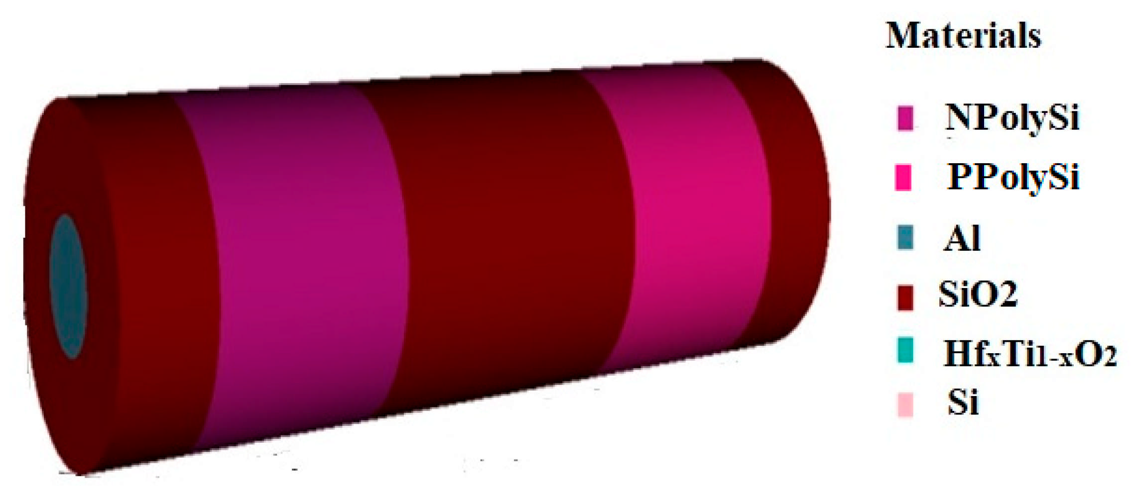
The structural description of ‘Device-III’ with a channel length of 21 nm, variable high-k gate dielectric values, and an 8 nm radius is presented in Figure 2. Figure 3a,b show the 3D cubic depiction of ‘Device-I’ and ‘Device-II’. The 3D cubic depiction of ‘Device-III’ is displayed in Figure 4. For the proposed devices (‘Device-I’, ‘Device-II’, and ‘Device-III’), the metal work function of the gate was maintained at 4.8 eV and 4.67 eV, respectively. Due to the employment of Schottky metal contacts with permissible work functions, such as 4.2 eV for ‘Device-I’ and 5.3 eV for ‘Device-II’ and ‘Device-III’, the proposed device became a single mask device, eliminating the need for a mask in the source/drain area [22]. The simulation parameters of the proposed ‘Device-I’ were calibrated at room temperature (300 K). Figure 5 outlines the comparison of the simulated work with the existing work to inspect the validity of the TCAD simulator [27]. Figure 6a displays the transfer characteristics of ‘Device-I’ and ‘Device-II’ at different Vd voltages as the gate voltage (Vg) varied from −1.0 V to 1.0 V. Figure 6b outlines the transfer characteristics of ‘Device-I’ and ‘Device-III’ at Vd = 0.1 V, 0.5 V, 0.8 V, and 1.0 V as the gate voltage (Vg) varied from −1.0 V to 1.0 V. It has been noted that ‘Device-I’ has a larger drain current compared to ‘Device-II’ because holes have lower mobility compared to electrons [28]. It can be observed in Figure 6b that ‘Device-III’ produces the same drain current as ‘Device-I’ because of the larger area of ‘Device-III’ compared to ‘Device-I’. The output curves for ‘Device-I’, ‘Device-II’, and ‘Device-III’ are displayed in Figure 7.
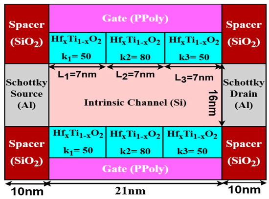
Figure 2.
Two-dimensional structural description of ‘Device-III’ for k1 = 50, k2 = 80, and k3 = 50.
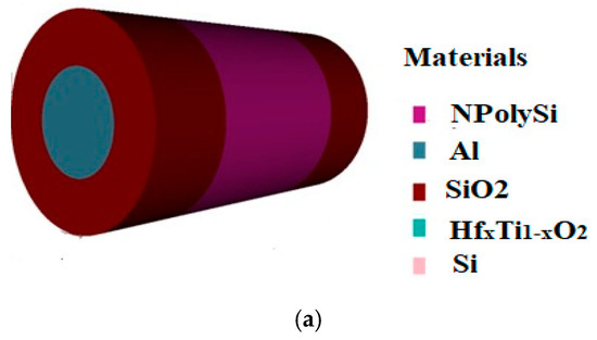
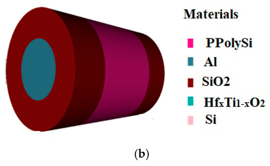
Figure 3.
Three-dimensional cubic depiction of (a) ‘Device-I’ and (b) ‘Device-II’.

Figure 4.
Three-dimensional cubic depiction of ‘Device-III’.
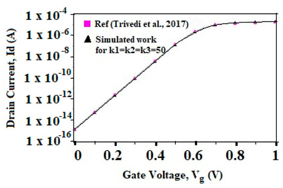
Figure 5.
Device calibration utilizing drain current (Id) versus gate voltage (Vg) [27].
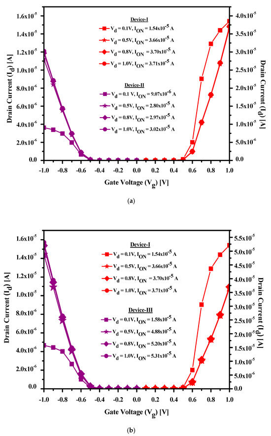
Figure 6.
Transfer curves of (a) ‘Device-I’ and ‘Device-II’ and (b) ‘Device-I’ and ‘Device-III’ at a drain voltage (Vd) equal to 0.1 V, 0.5 V, 0.8 V, and 1.0 V.
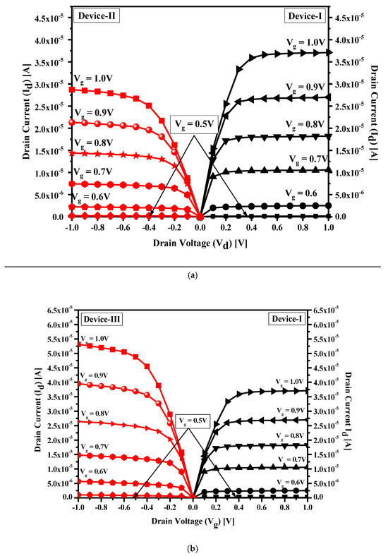
Figure 7.
Output curves of (a) ‘Device-I’ and ‘Device-II’ and (b) ‘Device-I’ and ‘Device-III’ at different gate voltage (Vg) and drain voltage (Vd) values from −1.0 V to 1.0 V for 21 nm channel length.
Device Physics
The following approved models were used to create the proposed structures:
- The Drift-Diffusion Model (DDML) is used to create a sequence of Poisson equations. It is strong and works instantly for the created structures.
- The ‘φ’ symbol represents the electron charge, the ‘q’ symbol indicates the electrostatic charge of the vacuum level and and represent the doping ionized proportion. The number of holes is denoted by ‘p’ and the number of electrons is indicated by ‘n’.
- Monitoring the carrier’s motion in the device’s inverted layer serves as a role model for Lombardi’s mobility. The combined mobility of doped carriers is outlined below:
The phrase ‘µB’ represents “bulk mobility”, ‘µAC’ indicates “degradation/scattering mobility” and “Surface roughness” is represented by the symbol ‘µSR’.
- Kane’s model for band-to-band tunneling-based carrier generation is represented in Equation (3).
The factors ‘A.BBT’ and ‘B.BBT’ represent experimentally measured fitting elements, and the ‘EG’ parameter represents a bandgap energy that follows an electric field (‘E’).
- The aforementioned process for the Shockley Read Hall (SRH) recombination with carriers examines the mutation rate and is shown below:
Here, ‘’ represents the intrinsic density of the carriers; ‘ET’ represents the captured energy level and the carrier longevity, and the lattice thermal is indicated by ‘’, and ‘TL’ respectively [17,22].
3. Inverters Design Structure and Simulation
Table 2 displays the design parameters used for the proposed inverters. The two CMOS inverters, i.e., Inverter-1 and Inverter-2, were created using proposed devices such as ‘Device-I’, ‘Device-II’, and ‘Device-III’.
Table 2.
Specifications of proposed inverters.
Inverter-1 was designed using devices ‘Device-I’ and ‘Device-II’. The selected tunable high-k oxide (HfxTi1−xO2) values for different regions of the channel are as follows, i.e., ‘k1’ = 50 for the ‘L1’ channel length, ‘k2’ = 80 for the ‘L2’ channel length, and ‘k3’ = 50 for the ‘L3’ channel length. Similarly, Inverter-2 was designed using ‘Device-I’ and ‘Device-III’ by choosing different values of tunable (HfxTi1−xO2) high-k oxide materials for different regions of the channel, i.e., ‘k1’ = 50 for the ‘L1’ channel length, ‘k2’ = 80 for the ‘L2’ channel length, and ‘k3’ = 50 for the ‘L3’ channel length. The 2D configurations of Inverter-1 and Inverter-2 are displayed in Figure 8 and Figure 9, respectively.
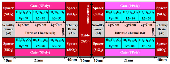
Figure 8.
Two-dimensional image of the optimized Inverter-1 with ‘Device-I’ and ‘Device-II’ for k1 = 50, k2 = 80, and k3 = 50.
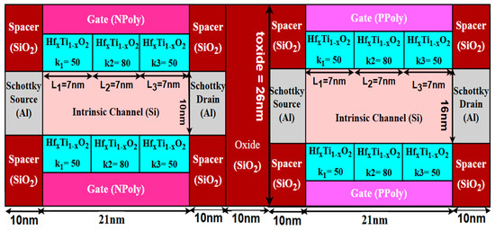
Figure 9.
Two-dimensional image of the optimized Inverter-2 with ‘Device-I’ and ‘Device-III’ for k1 = 50, k2 = 80, and k3 = 50.
Aluminum metal was used for the construction of the source/drain terminals of the proposed devices (‘Device-I’, ‘Device-II’, and ‘Device-III’). HfxTi1−xO2 oxide was utilized as a gate dielectric, while SiO2 oxide was used as a spacer. An intrinsic silicon channel was formed between the source/drain terminals for the design of devices such as ‘Device-I’, ‘Device-II’, and ‘Device-III’. The gate material used to cover the high-k gate oxides was ‘Npoly silicon’ for ‘Device-I’ and ‘Ppoly silicon’ for ‘Device-II’ and ‘Device-III’. The optimized 3D structures of Inverter-1 and Inverter-2 are displayed in Figure 10 and Figure 11, respectively.
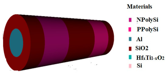
Figure 10.
Three-dimensional isometric image of optimized Inverter-1 developed using ‘Device-I’ and ‘Device-II’.
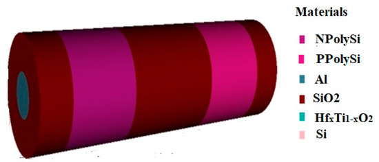
Figure 11.
Three-dimensional isometric image of optimized Inverter-2 using ‘Device-I’ and ‘Device-III’.
4. Results and Discussion
The COGENDA TCAD 3D Device Simulator is utilized for designing devices such as ‘Device-I’, ‘Device-II’, and ‘Device-III’ and their inverters (Inverter-1 and Inverter-2). The following models of the ‘Drift-Diffusion model’, the ‘Lombardi mobility model’, the ‘SRH carrier recombination mechanism’, and ‘Kane’s model’ were utilized to create and simulate the proposed devices and circuits [22].
Digital parameters like ‘ON-current’ (ION), ‘OFF-current’ (IOFF), ‘Current Ratio’ (ION/IOFF), and SCEs such as ‘Sub-Threshold Swing’ (SS) and ‘drain-induced barrier lowering’ (DIBL) were evaluated for the proposed devices. Performance analog parameters such as ‘Transconductance’ (gm), ‘Transconductance Generation Factor’ (TGF = gm/Id), ‘Output Conductance’ (gd), and ‘Early Voltage’ (Id/gd) were calculated for the designed structure. The DC and the transient analysis of optimized inverters designed with the proposed devices (‘Device-I’, ‘Device-II’, and ‘Device-III’) were also measured in the TCAD environment.
4.1. Device: Analysis of Electrical Characteristics and SCEs
The ON-current (ION) of the proposed devices was calculated at Vd = 0.1 V, Vg = 1.0, V, and the OFF-current (IOFF) was measured at Vd = 0.1 V, Vg = 0 V. It has been observed in Table 3 that the ‘Device-I’ has more ION and less IOFF compared to ‘Device-II’ and ‘Device-III’.
Table 3.
Comparative analysis of ‘Device-I’, ‘Device-II’, and ‘Device-III’ for k1 = 50, k2 = 80, k3 = 50 at Vd = 0.1 V, and Vg = 1.0 V at 21 nm channel length.
‘Device-I’ had a 55.8% greater ION/IOFF ratio compared to ‘Device-II’. ‘Device-III’ had 66.1% more IOFF compared to ‘Device-I’ and, thus, had a reduced ION/IOFF ratio by 33 times. The switching performance of devices was evaluated using SS. The SS depicts how the drain current behaves in the sub-threshold zone. It is calculated by dividing the decade change in the drain current by the change in the gate voltage, as mentioned in Equation (5). The measurement unit of SS is mV/dec.
The optimal value of SS at 300 K is 60 mV/dec. The extracted values for both ‘Device-I’ and ‘Device-II’ were obtained near the ideal value, as mentioned in Table 3. When the potential barrier drops and the drain voltage increases, this phenomenon is referred to as DIBL. Reduced DIBL, i.e., 8.2 mV/V, 8 mV/V, and 39 mV/V, was calculated for ‘Device-I’, ‘Device-II’, and ‘Device-III’, respectively, compared to ideal DIBL (100 mV/V). As the gate dielectric high-k value increases, the gate capacitance also increases, which results in a reduction in SS and DIBL [29,30,31,32,33,34,35,36]. Therefore, such devices are suitable for implementing digital VLSI circuits.
4.2. Device: Analysis of Analog Parameters
The analog parameter transconductance (gm) measures the device’s voltage conversion capability into current. The mathematical formula for calculating the gm is expressed in Equation (6).
Table 4 shows the largest gm (7.03 × 10⁻⁵ S) for ‘Device-I’ compared to ‘Device-II’ and ‘Device-III’. A smaller bandgap and better control over the channel through the gate terminal are indicated by a higher value of gm. Figure 12a presents the fluctuation in gm with respect to gate voltage (Vg) at various drain voltages (Vd), i.e., 0.1 V to 1.0 V [26]. The formula gm/Id was utilized to obtain the transconductance Generation Factor (TGF), which is another Figure of Merit that shows how efficiently a device converts current into transconductance. Figure 12b shows the variation in TGF with respect to Vg for Vd = 0.1 V and 1.0 V. It can be observed from Figure 12b that the same value of TGF, i.e., 10 V−1 was extracted for ‘Device-I’, ‘Device-II’ and ‘Device-III’. The output conductance (gd) was determined by dividing the change in drain current and the change in drain voltage, as expressed in Equation (7).
Table 4.
Comparative evaluation of analog performance of ‘Device-I’, ‘Device-II’, and ‘Device-III’.
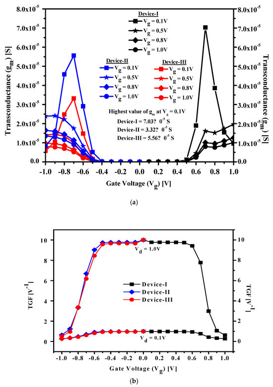
Figure 12.
(a) The gm variation with Vg from 0.1 V to 1.0 V, and (b) TGF variation with Vg at drain voltages (Vd) = 0.1 V and 1.0 V for ‘Device-I’, ‘Device-II’, and ‘Device-III’.
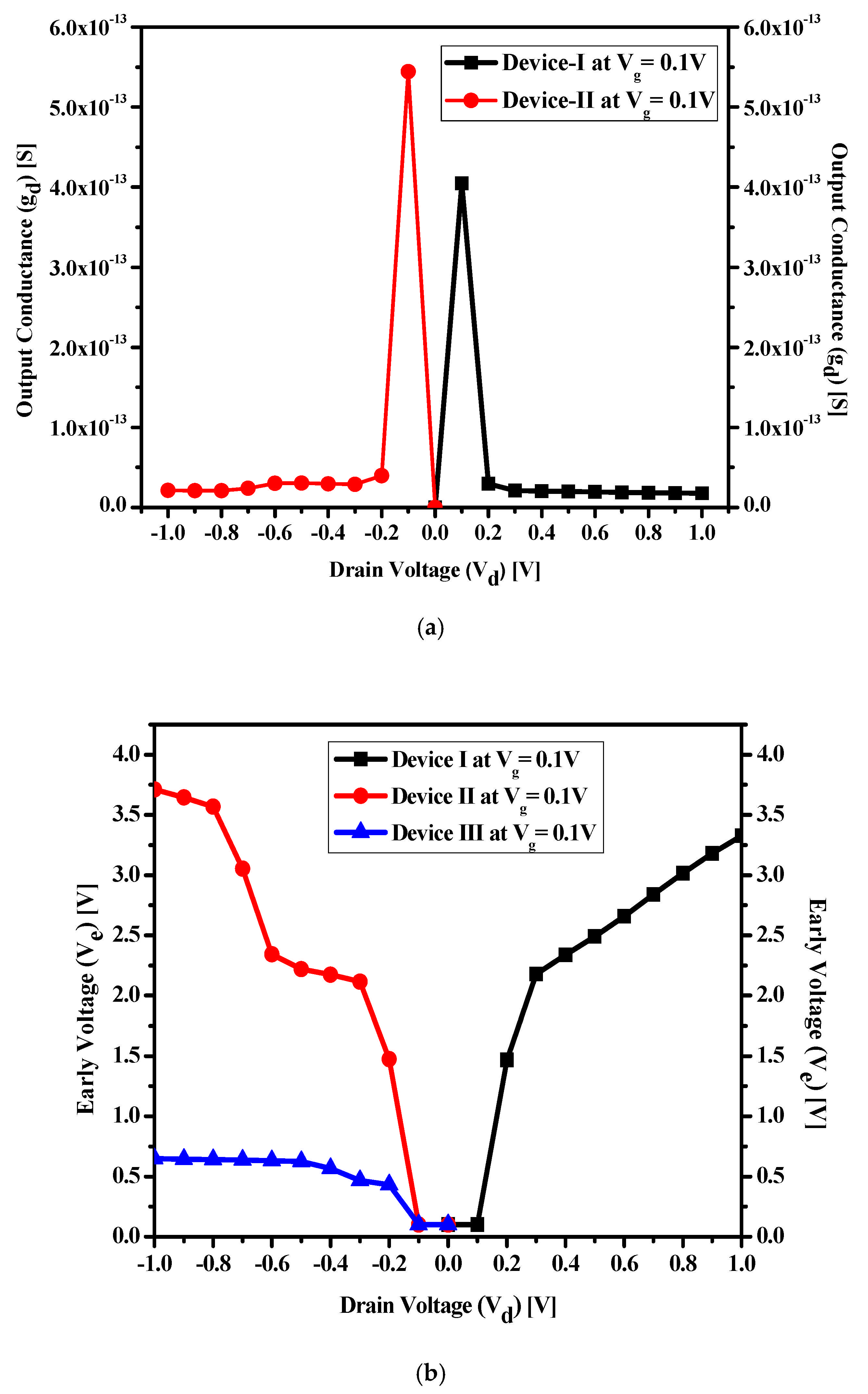
The lowest value of gd is 1.77 × 10⁻¹⁴ S, which was measured for ‘Device-I’, as shown in Table 4. The smaller value of gd improves the analog performance parameters, such as the early voltage (Ve) and intrinsic gain (A) of devices. Figure 13a outlines the variation in gd with respect to Vd for Vg = 0.1 V.
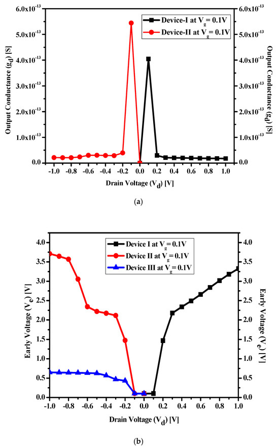
Figure 13.
(a) The gd variation with Vd, and (b) Ve variation with Vd at the gate voltage (Vg) = 0.1 V for ‘Device-I’, ‘Device-II’, and ‘Device-III’.
4.3. Comparative Analysis of Proposed Devices with the Existing Literature
Table 5 indicates the contrast between the optimized proposed devices of channel length 21 nm with an existing device of channel length 20 nm. It is noted that ‘Device-I’ exhibited a 3.25% improvement in SS, a 61.46% decrement in DIBL, and a 2.29 times enhancement in ION/IOFF compared to the device designed by Kaur et al., 2019. For ‘Device-II’, the performance parameter ION/IOFF increased by 2.57 times compared to the P-Channel device created by the author in [24]. The switching parameters SS and DIBL of ‘Device-II’ were reduced by 4.15% and 68.89%, respectively, compared to the work performed by Kaur et al., 2019 [24]. It has been demonstrated that the designed devices have enhanced parameters and, thus, may be utilized to build low-power circuits [24].
Table 5.
Comparative analysis of optimized proposed devices with a channel length of 21 nm compared to existing devices with a channel length of 20 nm.
Table 6 demonstrates the performance analysis of proposed devices of 21 nm channel length with the device designed by Nayak et al., 2014. It is clear for ‘Device-I’ that the SS and DIBL parameters decreased by 8.44% and 83.60%, respectively, compared to the existing literature [37]. The DIBL showed a higher percentage decline compared to the work performed by Nayak et al., 2014, because of the use of compound gate dielectric material in the proposed devices. The ION/IOFF rose by a magnitude of 103, and gm increased by 32. 89% compared to the existing work [37].
Table 6.
Comparative analysis of designed devices with the existing device of channel length 17 nm.
Similarly, ‘Device-II’ exhibited a progressive improvement in the performance metrics when compared with the reference work [37]. In Table 6, it is observed that the proposed ‘Device-II’ shows an enhancement in ION/IOFF by 1000 times, and gm is increased by 47.36% compared to the device created by Nayak et al. in 2014. The other performance parameters, like SS and DIBL, also decreased by 15.89% and 87.87%, respectively, compared to the existing device of channel length 17 nm [37].
4.4. Optimized Inverters
It is clear from Table 4, Table 5 and Table 6 that the proposed devices, i.e., ‘Device-I’, ‘Device-II’, and ‘Device-III’, are suitable for implementing Inverter-1 and Inverter-2. Inverter-1 was built with ‘Device-I’ and ‘Device-II’ in the TCAD environment. Similarly, Inverter-2 was created with a combination of ‘Device-I’ and ‘Device-III’. The performance analysis of optimized inverters was performed by calculating the noise margin and transient analysis.
Transient Analysis and Noise Margin of Inverters
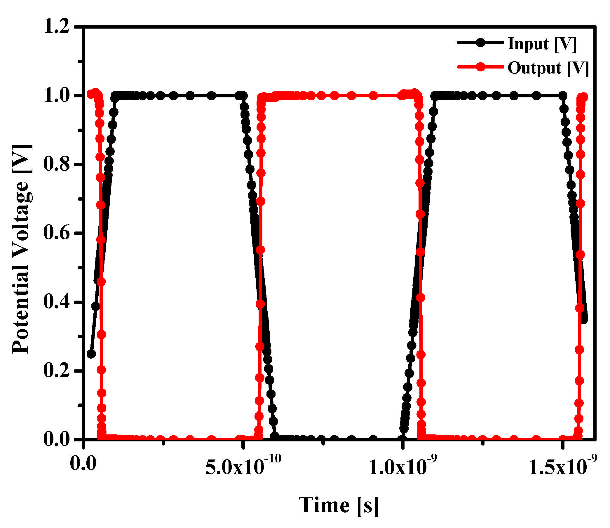
- Transient Analysis: It examines the behavior of circuits when they switch from one steady state to another state [28]. Figure 14 demonstrates the transient analysis of Inverter-1 at a supply voltage (VDD) of 1.0 V.
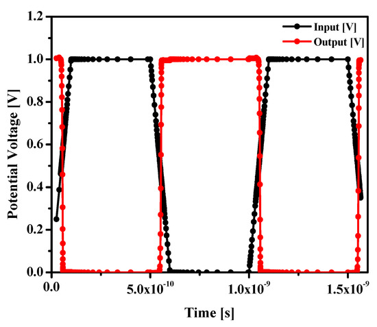 Figure 14. Transient simulation plot of Inverter-1 at VDD 1.0 V.
 - Noise Margin: The noise margin determines the noise immunity of circuits, and this is indicated by NM [29]. The circuit with a higher value of NM shows high noise sensitivity. The expression for calculating NM for low signals (NML) and for high signals (NMH) is expressed as follows:
NML = VIL − VOL
NMH = VOH − VIH
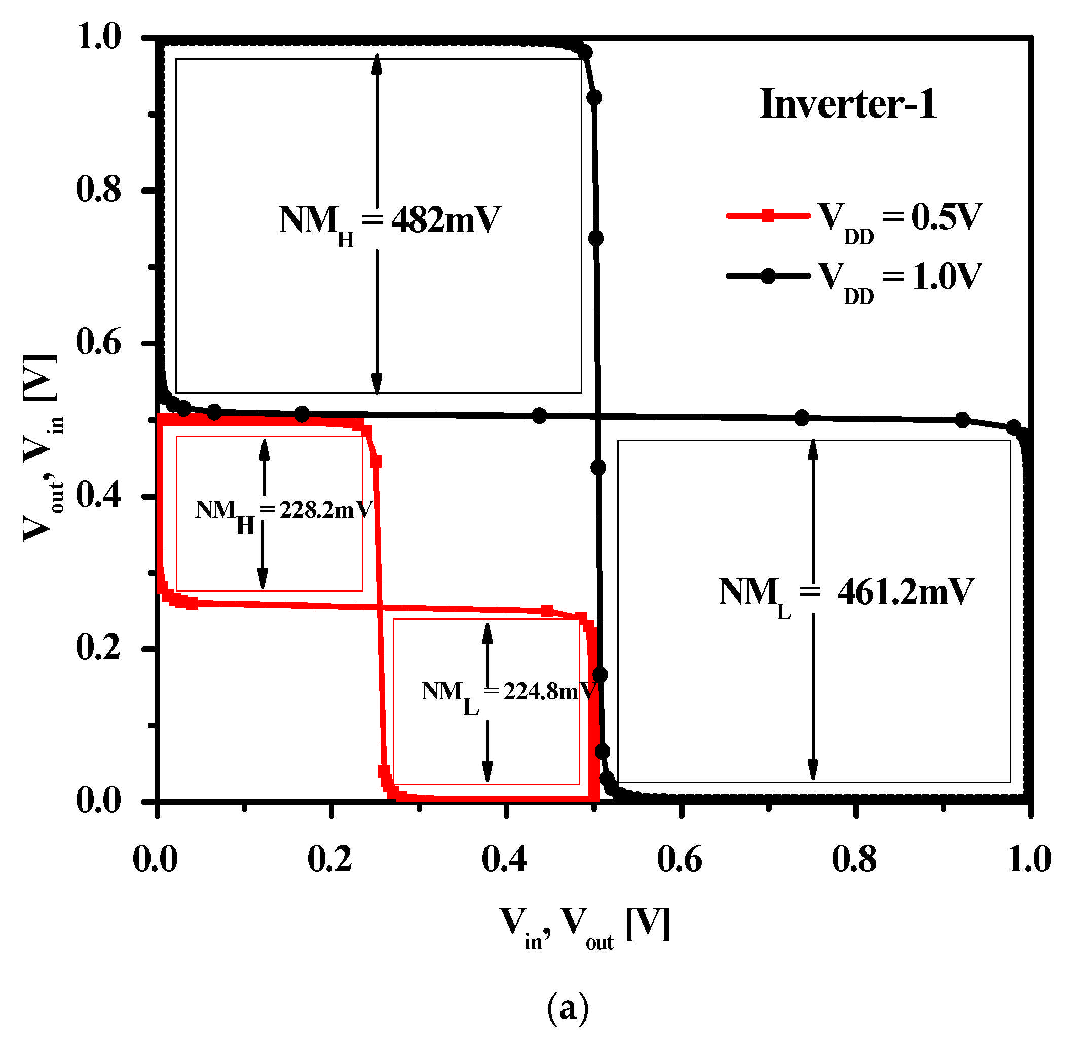
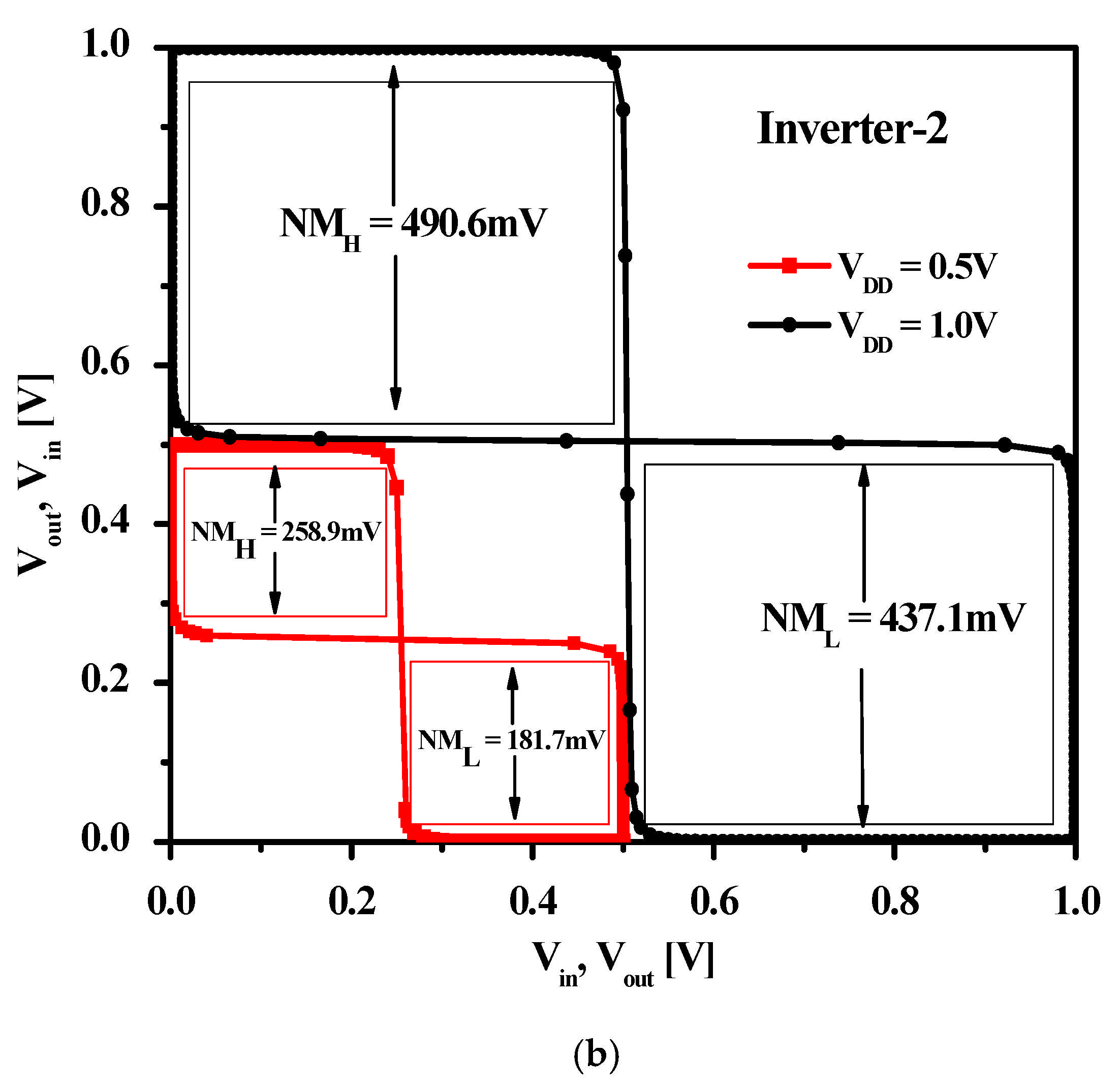
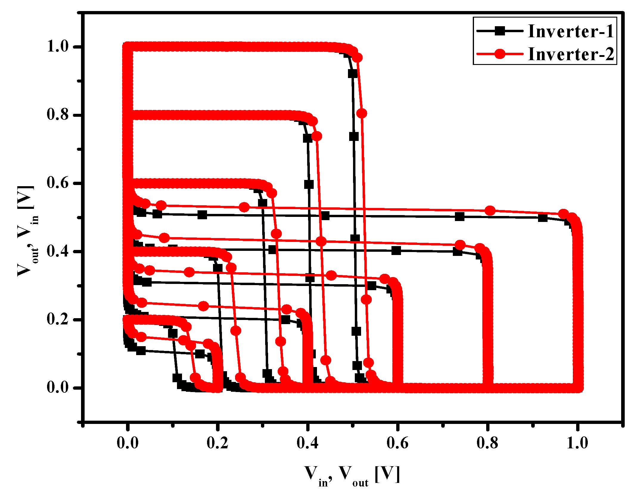
The lowest output value at logic level 0 is represented by VOL, and the highest output voltage at logic level 1 is represented by VOH [38]. Logic value 0 designates the lowest input voltage (VIL), while logic value 1 designates the highest input voltage (VIH). Figure 15 demonstrates the butterfly curve of Inverter-1 and Inverter-2 at supply voltage levels of 0.5 V and 1.0 V. The calculated noise margin values, i.e., NMH = 482 mV and NML = 461.2 mV of Inverter-1, are demonstrated in Figure 15a. Figure 15b displays the NM values for Inverter-2. The lowest output value at logic level 0 is represented by VOL, and the highest output voltage at logic level 1 is represented by VOH [38]. Logic value 0 designates the lowest input voltage (VIL), while logic value 1 designates the highest input voltage (VIH). Figure 15 demonstrates the butterfly curve of Inverter-1 and Inverter-2 at supply voltage levels of 0.5 V and 1.0 V. The calculated noise margin values, i.e., NMH = 482 mV and NML = 461.2 mV of Inverter-1, are demonstrated in Figure 15a. Figure 15b displays the NM values for Inverter-2. Inverter-2 has a 1.78% higher NMH compared to the NMH of Inverter-1 at 1.0 V, and a similar scenario was observed at 0.5 V, i.e., Inverter-2 had 11.85% more NMH compared to Inverter-1. Inverter-1 presents a larger value of NML at both voltages compared to Inverter-2, as shown in Figure 15. The butterfly curves and calculated NM values for the variable voltage VDD from 0.2 V to 1.0 V of the proposed inverters are displayed in Figure 16 and Figure 17, respectively. It has been analyzed in both inverters that a higher supply voltage results in a higher NM.


Figure 15.
Butterfly curve of (a) Inverter-1 and (b) Inverter-2 at VDD 0.5 V and 1.0 V.
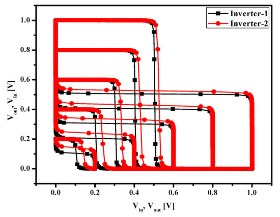
Figure 16.
Butterfly curve for proposed Inverter-1 and Inverter-2 at VDD variation from 0.2 V to 1.0 V.
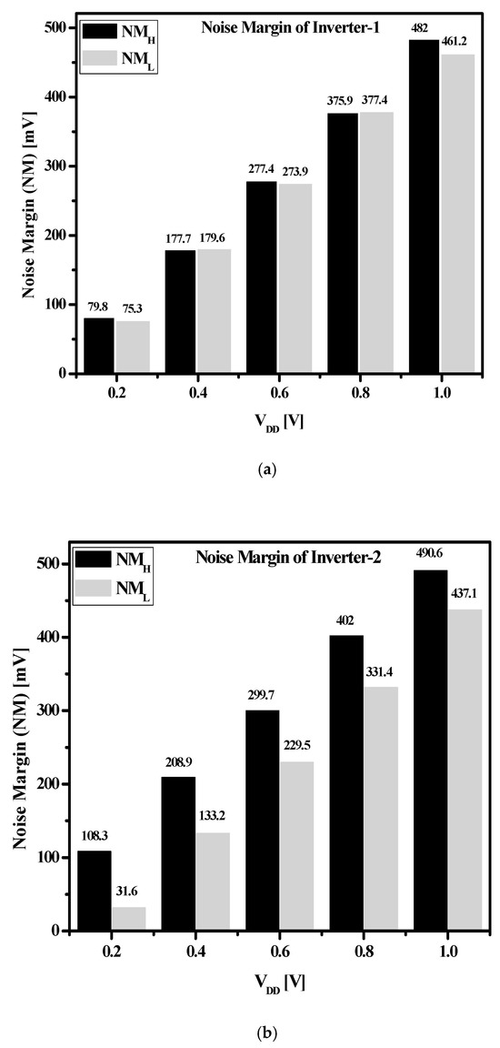
Figure 17.
Noise margin of (a) Inverter-1 and (b) Inverter-2 at variable VDD (0.2 V to 1.0 V).
4.5. Comparison of Designed Optimized Inverters with Previous Work
Table 7 expresses a 38% NMH improvement and 44% NML enhancement in Inverter-1 compared to the inverter designed by Nayak et al., 2014. Similarly, Inverter-2 presents a 40% and 37% greater value of NMH and NML, respectively, in comparison to the existing literature [37,38]. In the present work, the optimized devices used for implementing inverters were made with tunable HfxTi1−xO2 high-k gate dielectric materials. This improved the electrical and analog parameters and also reduced the SCEs, like the minimized values of SS and DIBL. Thus, it produced better functionality and greater noise immunity in the proposed inverters. Therefore, the proposed inverters are suitable for low-power applications.
Table 7.
Comparative analysis of proposed inverters to existing work.
5. Conclusions
Motivated by the need for further investigations into high-performance, energy-efficient semiconductor designs for emerging applications such as smart grids and smart cities, in this article, a potential design for a next-generation transistor called the Hetero-Dielectric Gate-All-Around (HD-GAA) MOSFET was created and investigated.
Specifically, the (HD-GAA) MOSFET is designed to be a next-generation transistor architecture candidate for sustainability, high-performance-embedded computing, and power control applications. Leveraging advanced materials like tunable high-k dielectrics (HfxTi1−xO2) and innovative GAA topologies, it has been shown in the studies presented herein that the proposed devices deliver enhanced performance, reduced power consumption, and scalability for modern applications in the semiconductor industry. Although further investigations are warranted, this article presents positive, supportive evidence of their suitability for deployment in the context of sustainable smart cities and smart grid applications.
Three devices (Device-I, Device-II, and Device-III) were designed in the COGENDA Visual TCAD environment, and their performance characteristics (ION, IOFF, ION/IOFF, SS, DIBL, gm, gd, and Ve) were evaluated. Device-I reduced SS and DIBL by 3.25%, 61.46%, and 8.44% compared to the existing literature. Device-I achieved an ION/IOFF improvement of 2.57 times and 1000 times and reduced SS and DIBL by 4.15% and 68.89%, respectively, compared to existing work.
Optimized inverters built with these devices showed significant noise margin enhancements. Inverter-1 improved NMH by 38% and NML by 44%, while Inverter-2 increased NMH and NML by 40% and 37%, respectively. These improvements highlight the suitability of the proposed devices for low-power digital and embedded systems applications, including SRAM, control circuitry for power converters and couplings, and other related logic circuits, making them a vital step toward a sustainable future in reducing carbon emissions in sustainable smart cities by using semiconductor industries. Future work will further develop and test the new device outlined in this work, and look to implement prototypes of low-cost, low-energy IoT end devices based upon its core design.
Author Contributions
Conceptualization, R.D. and G.K.; methodology, R.D., G.K. and A.S.; software, R.D. and G.K.; validation, R.D., G.K., A.S. and M.R.; formal analysis, R.D., G.K., A.S. and M.R.; investigation, R.D., G.K., A.S. and M.R.; resources, R.D., G.K., A.S. and M.R.; data curation, R.D., G.K., A.S. and M.R.; writing—original draft preparation, R.D., G.K., A.S. and M.R., writing—review and editing, R.D., G.K., A.S., M.R., G.A. and M.S.; visualization, R.D., G.K., A.S., M.R., G.A. and M.S.; supervision, R.D., G.K., A.S., M.R., G.A. and M.S. All authors have read and agreed to the published version of the manuscript.
Funding
This work has been partially supported and funded through the Enterprise Singapore, Product Development Grant (Ref: 23022ELD) to Teesside University, UK.
Data Availability Statement
The data samples were taken using TCAD simulations.
Acknowledgments
The authors would like to express their gratitude to MHRD, Govt. of India, for sanctioning the TEQIP-II grant to the Guru Nanak Dev Engineering College (GNDEC), Ludhiana. The authors would also like to thank the Principal, GNDEC, Ludhiana, for providing the necessary facilities in which to accomplish this research work. The authors would also like to thank Enterprise Singapore for sanctioning the Product Development Grant (Ref: 23022ELD) to Teesside University, UK which also helped to partially support this work.
Conflicts of Interest
The authors have no conflicts of interest to declare.
References
- Wang, R.; Jørgensen, A.B.; Dalal, D.N.; Luan, S.; Zhao, H.; Munk-Nielsen, S. Integrating 10-kV SiC MOSFET into battery energy storage system with a scalable converter-based self-powered gate driver. IEEE J. Emerg. Sel. Top. Power Electron. 2022, 11, 351–360. [Google Scholar] [CrossRef]
- Bhol, K.; Jena, B.; Nanda, U. Silicon nanowire GAA-MOSFET: A workhorse in nanotechnology for future semiconductor devices. Silicon 2022, 14, 3163–3171. [Google Scholar] [CrossRef]
- Duan, H. From MOSFET to FinFET to GAAFET: The evolution, challenges, and future prospects. Appl. Comput. Eng. 2024, 50, 113–120. [Google Scholar] [CrossRef]
- Jena, B.; Bhol, K.; Nanda, U. Exploration of Linearity Analysis in Nanotube GAA MOSFET Through Simulation-Based Study Utilizing Multi-Material Gate Technique. Trans. Electr. Electron. Mater. 2024, 25, 470–478. [Google Scholar] [CrossRef]
- Singh, A.P.; Kumar, A.; Chaudhary, B.S.; Tiwari, G.; Baghel, R.K.; Tirkey, S. Recessed-Source/Drain Junctionless GAA MOSFETs and their Sensitivity to Temperature: A Machine learning based Analysis. In Proceedings of the 2023 International Conference on Next Generation Electronics (NEleX), Vellore, Tamil Nadu, India, 14–16 December 2023; IEEE: New York, NY, USA, 2023; pp. 1–6. [Google Scholar]
- Kumar, C.M.; Mohan, Y.; Vimala, P. A study of gaa silicon nanowire mosfets for better performance. In Proceedings of the 2023 IEEE International Conference on Electronics, Computing and Communication Technologies (CONECCT), Nanning, China, 21–23 July 2023; IEEE: New York, NY, USA, 2023; pp. 1–4. [Google Scholar]
- Kumar, A.S.; Deekshana, M.; Sreenivasulu, V.B.; Kumari, N.A.; Shanthi, G. Device analysis of vertically stacked GAA nanosheet fet at advanced technology node. In Proceedings of the 2023 3rd International Conference on Advances in Computing, Communication, Embedded and Secure Systems (ACCESS), Ernakulam, India, 18–20 May 2023; IEEE: New York, NY, USA, 2023; pp. 274–279. [Google Scholar]
- Nagy, D.; Indalecio, G.; Garcia-Loureiro, A.J.; Elmessary, M.A.; Kalna, K.; Seoane, N. FinFET versus gate-all-around nanowire FET: Performance, scaling, and variability. IEEE J. Electron. Devices Soc. 2018, 6, 332–340. [Google Scholar] [CrossRef]
- Yadav, R.; Ahuja, K.; Rathee, D.S. Performance enhancement of GAA multi-gate nanowire with asymmetric hetero-dielectric oxide. Silicon 2022, 14, 1935–1946. [Google Scholar] [CrossRef]
- Lee, Y.; Park, G.-H.; Choi, B.; Yoon, J.; Kim, H.-J.; Kim, D.H.; Kim, D.M.; Kang, M.-H.; Choi, S.-J. Design study of the gate-all-around silicon nanosheet MOSFETs. Semicond. Sci. Technol. 2020, 35, 03LT01. [Google Scholar] [CrossRef]
- Kumar, M.; Haldar, S.; Gupta, M.; Gupta, R.S. Impact of gate material engineering (GME) on analog/RF performance of nanowire Schottky-barrier gate all around (GAA) MOSFET for low power wireless applications: 3D T-CAD simulation. Microelectron. J. 2014, 45, 1508–1514. [Google Scholar] [CrossRef]
- Veshala, M.; Jatooth, R.; Reddy, K.R. Reduction of short-channel effects in FinFET. Int. J. Eng. Innov. Technol. (IJEIT) 2013, 2, 118–124. [Google Scholar]
- Madan, J.; Gupta, R.S.; Chaujar, R. Performance investigation of heterogeneous gate dielectric-gate metal engineered–gate all around-tunnel FET for RF applications. Microsyst. Technol. 2017, 23, 4081–4090. [Google Scholar] [CrossRef]
- Semiconductor Digest News and Industry Trends. IBM Announces 2 nm GAA FET Technology. Available online: https://www.semiconductor-digest.com/ibm-announces-2nm-gaa-fet-technology-the-sum-of-aha-moments/ (accessed on 16 January 2025).
- Mukesh, S.; Zhang, J. A review of the gate-all-around nanosheet FET process opportunities. Electronics 2022, 11, 3589. [Google Scholar] [CrossRef]
- Rewari, S.; Nath, V.; Haldar, S.; Deswal, S.S.; Gupta, R.S. Gate-induced drain leakage reduction in the cylindrical dual-metal hetero-dielectric gate all around MOSFET. IEEE Trans. Electron. Devices 2017, 65, 3–10. [Google Scholar] [CrossRef]
- Ghosh, S.; Pachal, P.; Kumar, R.; Kundu, S.; Ghosh, J.; Sarkar, S.K. Double gate pnpn TFET with hetero oxide dielectric and high-k spacer engineering. In Proceedings of the 2020 IEEE Vlsi Device Circuit and System (Vlsi Dcs), Kolkata, India, 18–19 July 2020; IEEE: New York, NY, USA, 2020; pp. 1–5. [Google Scholar]
- Intel Corporation. Shaping the Future of Technology. Investor Relations. Intel. Available online: https://www.intc.com/news-events/press-releases (accessed on 15 January 2025).
- IBM—United Kingdom. Available online: https://www.ibm.com (accessed on 14 January 2025).
- TSMC. Available online: https://n2.tsmc.com/english/dedicatedFoundry/technology/N2.htm (accessed on 15 January 2025).
- Samsung Semiconductor Global. In: Samsung Semiconductor Global. Available online: https://semiconductor.samsung.com/ (accessed on 15 January 2025).
- Yousf, M.; Singh, N.G.; Kaur, G. Impact of Work Function and Temperature Variation on Schottky barrier Hetero-Dielectric Gate All Around Nanowire Field Effect Transistor. J. Emerg. Technol. Innov. Res. 2022, 9. Available online: https://www.jetir.org/papers/JETIRFQ06032.pdf (accessed on 15 January 2025).
- Cutress I Intel’s Process Roadmap to 2025: With 4 nm, 3 nm, 20A and 18A?! Available online: https://www.anandtech.com/show/16823/intel-accelerated-offensive-process-roadmap-updates-to-10nm-7nm-4nm-3nm-20a-18a-packaging-foundry-emib-foveros (accessed on 15 January 2025).
- Kaur, A.; Mehra, R.; Saini, A. Hetero-dielectric oxide engineering on dopingless gate all around nanowire MOSFET with Schottky contact source/drain. AEU-Int. J. Electron. Commun. 2019, 111, 152888. [Google Scholar] [CrossRef]
- Hosoi, T.; Minoura, Y.; Asahara, R.; Oka, H.; Shimura, T.; Watanabe, H. Schottky source/drain germanium-based metal-oxide-semiconductor field-effect transistors with self-aligned NiGe/Ge junction and aggressively scaled high-k gate stack. Appl. Phys. Lett. 2015, 107, 252104. [Google Scholar] [CrossRef]
- Roy, N.; Gupta, A.; Rai, S. Analytical surface potential modeling and simulation of junction-less double gate (JLDG) MOSFET for ultra-low-power analog/RF circuits. Microelectron. J. 2015, 46, 916–922. [Google Scholar] [CrossRef]
- Trivedi, N.; Kumar, M.; Haldar, S.; Deswal, S.S.; Gupta, M.; Gupta, R. Charge plasma technique based dopingless accumulation mode junctionless cylindrical surrounding gate MOSFET: Analog performance improvement. Appl. Phys. A 2017, 123, 546. [Google Scholar] [CrossRef]
- Basic Electronics Tutorials. Available online: https://www.electronics-tutorials.ws/transistor/tran_6.html (accessed on 15 January 2025).
- Devi, R.; Kaur, G. Design of Hetero-Dielectric Single-Metal Gate-All-Around MOSFET with Schottky Contact Source/Drain; Springer: Singapore, 2023; pp. 1–10. [Google Scholar] [CrossRef]
- Pradhan, K.P.; Mohapatra, S.K.; Sahu, P.K.; Behera, D.K. Impact of high-k gate dielectric on analog and RF performance of nanoscale DG-MOSFET. Microelectron. J. 2014, 45, 144–151. [Google Scholar] [CrossRef]
- Gupta, P.K.; Upadhyay, A.K.; Jha, C.K.; Gupta, A.; Gupta, L. Performance analysis and comparison of different High-K materials used as gate dielectrics in DH-TMSG MOSFET. Int. J. Res. Appl. Sci. Eng. Technol. 2022, 10, 1870–1889. [Google Scholar] [CrossRef]
- Bendib, T.; Djeffal, F.; Meguellati, M. An optimized junctionless GAA MOSFET design based on multi-objective computation for high-performance ultra-low power devices. J. Semicond. 2014, 35, 074002. [Google Scholar] [CrossRef]
- Hu, G.; Tang, T.-A.; Wang, L.; Liu, R.; Ding, Z.; Xiang, P. Analytical Models for Electric Potential, Threshold Voltage, and Subthreshold Swing of Junctionless Surrounding-Gate Transistors. IEEE Trans. Electron. Devices 2014, 61, 688–695. [Google Scholar] [CrossRef]
- Liu, T.Y.; Sheu, J.T.; Pan, F.M. Characteristics of Gate-All-Around Junctionless Polysilicon Nanowire Transistors with Twin 20-nm Gates. IEEE J. Electron. Devices Soc. 2015, 3, 405–409. [Google Scholar] [CrossRef]
- Xu, L.; Wu, G.; Li, P.; Cheng, T. Modeling threshold voltage and drain-induced barrier lowering effect of opposite doping core–shell channel surrounding-gate junctionless MOSFET. Microelectron. J. 2023, 139, 105830. [Google Scholar] [CrossRef]
- Robertson, J. High dielectric constant oxides. Eur. Phys. J. -Appl. Phys. 2004, 28, 265–291. [Google Scholar] [CrossRef]
- Nayak, K.; Bajaj, M.; Konar, A.; Oldiges, P.J.; Natori, K.; Iwai, H.; Rao, V.R. CMOS logic device and circuit performance of Si gate all around nanowire MOSFET. IEEE Trans. Electron Devices 2014, 61, 3066–3074. [Google Scholar] [CrossRef]
- ChipEdge VLSI Training Company. Available online: https://chipedge.com/discover-what-is-noise-margin-in-vlsi/ (accessed on 16 January 2025).


Disclaimer/Publisher’s Note: The statements, opinions and data contained in all publications are solely those of the individual author(s) and contributor(s) and not of MDPI and/or the editor(s). MDPI and/or the editor(s) disclaim responsibility for any injury to people or property resulting from any ideas, methods, instructions or products referred to in the content. |
© 2025 by the authors. Licensee MDPI, Basel, Switzerland. This article is an open access article distributed under the terms and conditions of the Creative Commons Attribution (CC BY) license (https://creativecommons.org/licenses/by/4.0/).