

Polarization Doping in a GaN-InN System—Ab Initio Simulation

 , , ,
, , ,  , , , , ,
  and
and 
Abstract
:1. Introduction
2. Methods
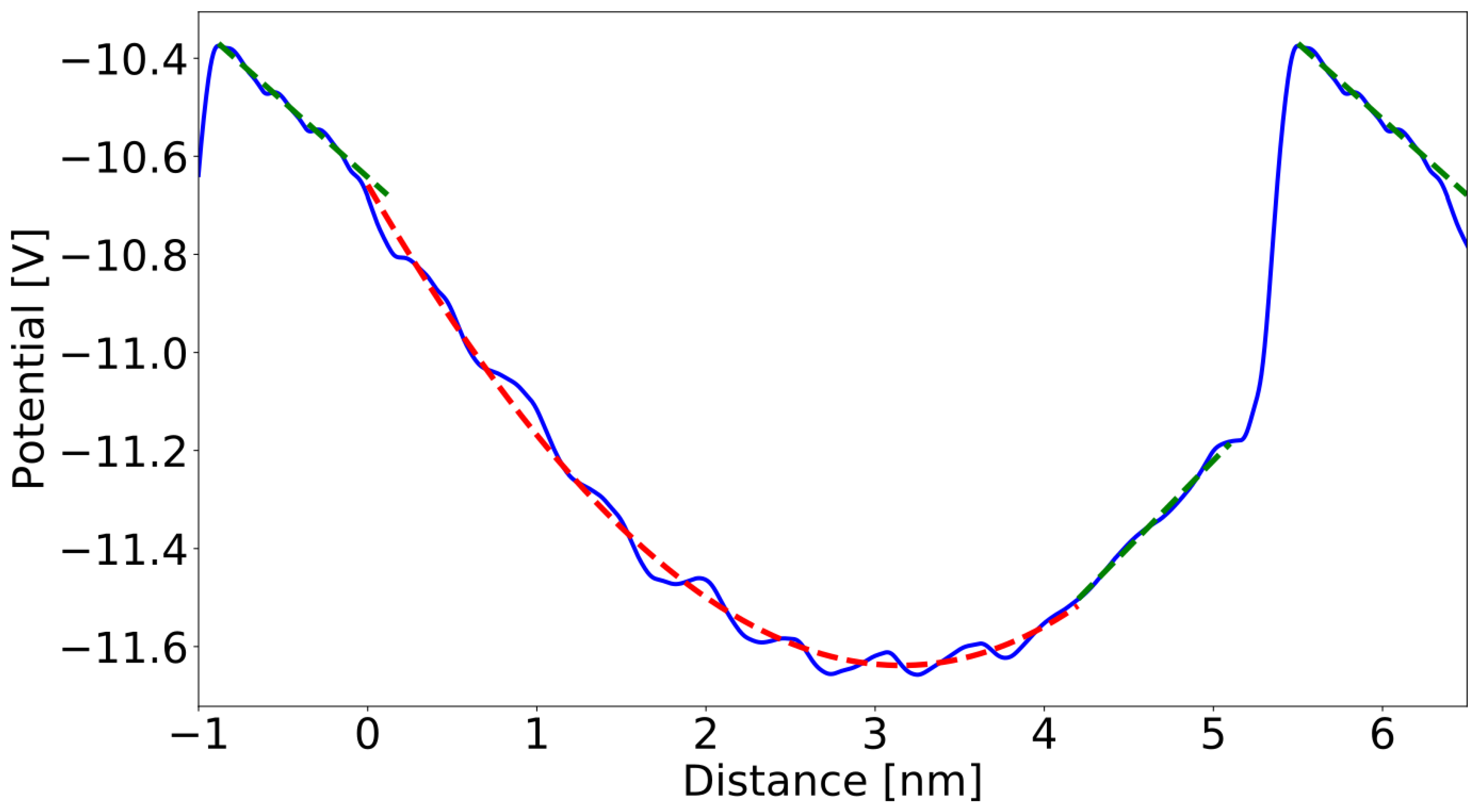
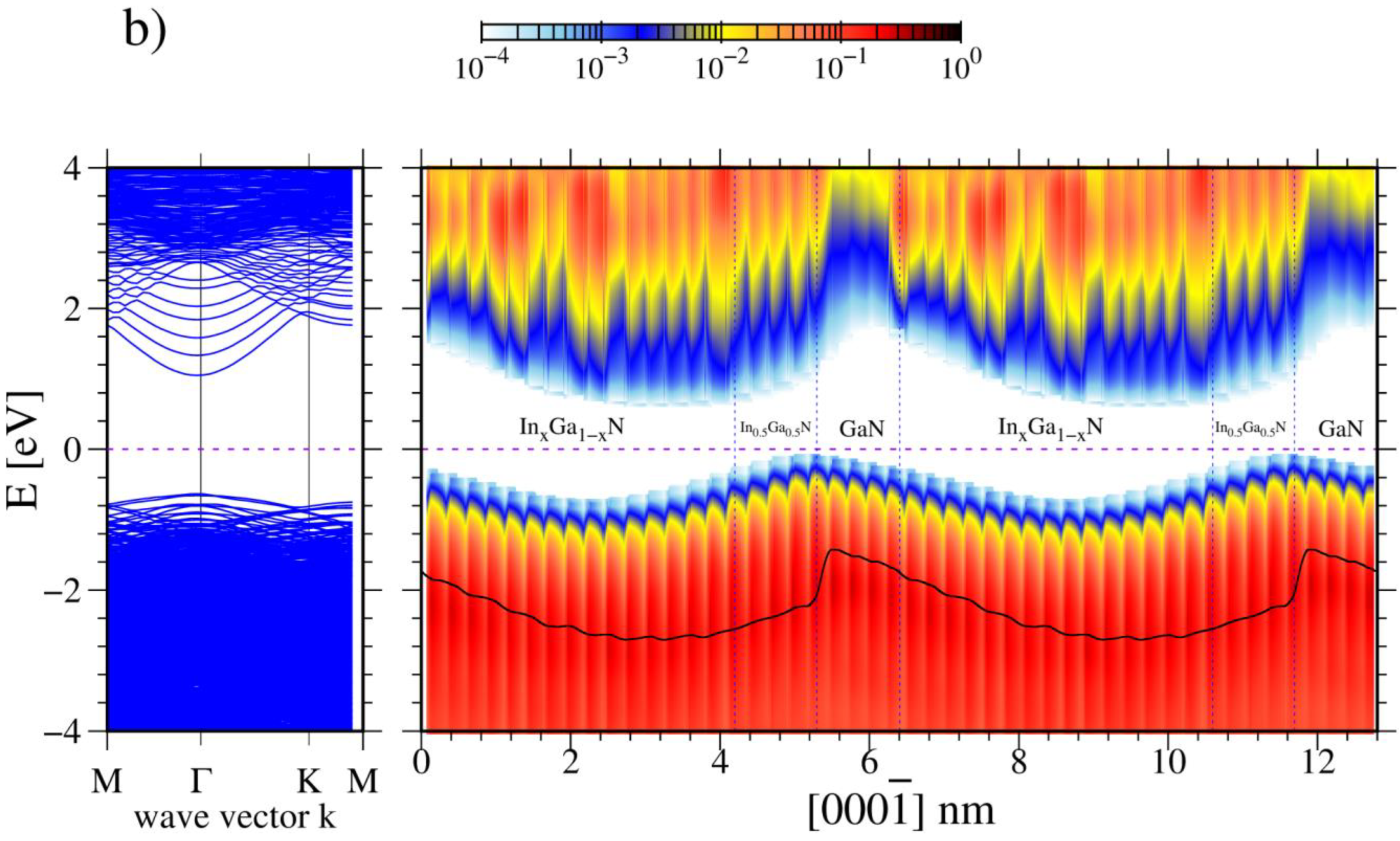
3. Results
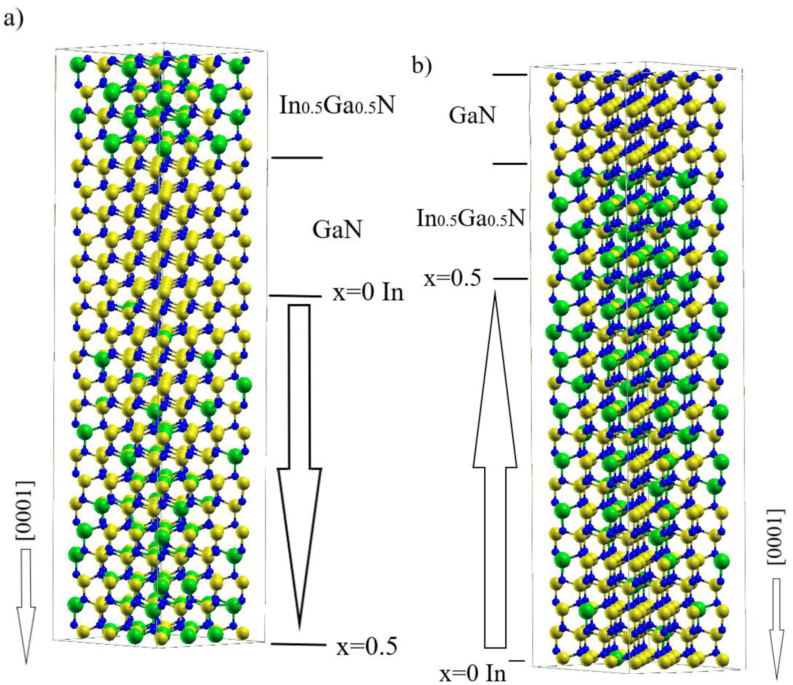
- (i)
- Four Ga-N double atomic layers (metal and nonmetal layers);
- (ii)
- Four In0.5Ga0.5N double atomic layers (metal and nonmetal layers);
- (iii)
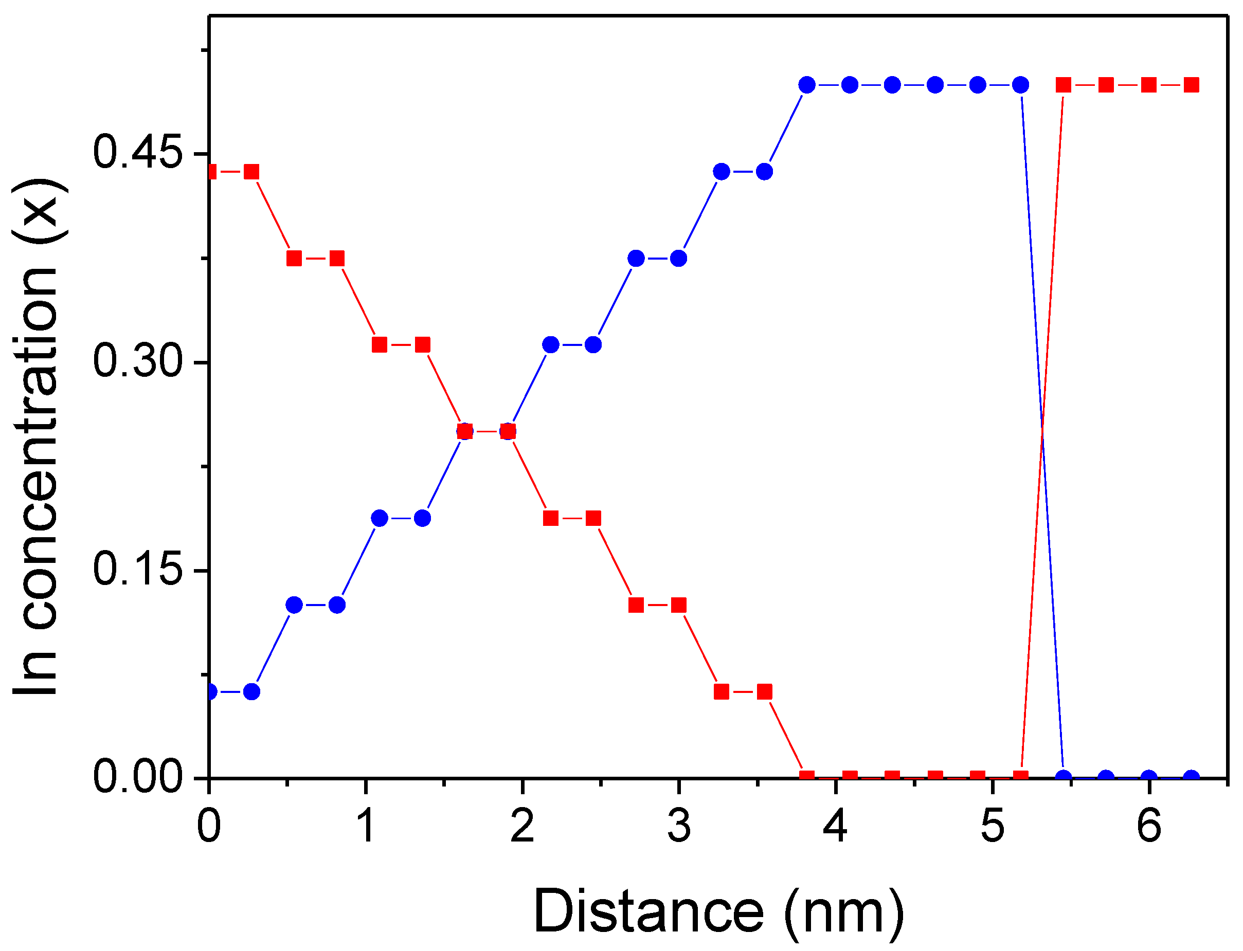
- Sixteen linearly graded Ga-In-N double atomic layers, with Ga content increasing or decreasing along [0001] direction (metal layers composed of Ga and In, nonmetal layer composed of N).
4. Conclusions
Author Contributions
Funding
Institutional Review Board Statement
Informed Consent Statement
Data Availability Statement
Conflicts of Interest
References
- Landau, L.D.; Lifshitz, E.M.; Sykes, J.B.; Bell, J.S.; Dill, E.H. Electrodynamics of Continuous Media; Pergamon Press: Oxford, UK, 1984. [Google Scholar]
- Feneberg, M.; Thonke, K. Polarization fields of III-nitrides grown in different crystal orientations. J. Phys. Condens. Matter 2007, 19, 403201. [Google Scholar] [CrossRef] [PubMed]
- Zúñiga-Pérez, J.; Consonni, V.; Lymperakis, L.; Kong, X.; Trampert, A.; Fernández-Garrido, S.; Brandt, O.; Renevier, H.; Keller, S.; Hestroffer, K.; et al. Polarity in GaN and ZnO: Theory, measurement, growth, and devices. Appl. Phys. Rev. 2016, 3, 041303. [Google Scholar] [CrossRef] [Green Version]
- Ashcroft, N.W.; Mermin, N.D. Solid State Physics; Thomson Learning: Toronto, ON, Canada, 1976. [Google Scholar]
- Monch, W. Semiconductor Surfaces and Interfaces; Springer: Berlin/Heidelberg, Germany, 1993. [Google Scholar]
- Eller, B.S.; Yang, J.; Nemanich, R.J. Electronic surface and dielectric interface states on GaN and AlGaN. J. Vac. Sci. Technol. A Vac. Surf. Film. 2013, 31, 050807. [Google Scholar] [CrossRef]
- Miller, D.A.B.; Chemla, D.S.; Damen, T.C.; Gossard, A.C.; Wiegmann, W.; Wood, T.H.; Burrus, C.A. Band-edge electroabsorption in quantum well structures—The quantum confined Stark effect. Phys. Rev. Lett. 1984, 53, 2173–2176. [Google Scholar] [CrossRef]
- Halsall, M.P.; Nicholls, J.E.; Davies, J.J.; Cockayne, B.; Wright, P.J. CdS/CdSe wurtzite intrinsic Stark superlattices. J. Appl. Phys. 1992, 71, 907–915. [Google Scholar] [CrossRef]
- Kaminska, A.; Strak, P.; Borysiuk, J.; Sobczak, K.; Domagala, J.Z.; Beeler, M.; Grzanka, E.; Sakowski, K.; Krukowski, S.; Monroy, E. Correlation of optical and structural properties of GaN/AlN multi-quantum wells—Ab initio and experimental study. J. Appl. Phys. 2016, 119, 015703. [Google Scholar] [CrossRef]
- Waltereit, P.; Brandt, O.; Trampert, A.; Grahn, H.T.; Menniger, J.P.; Ramsteiner, M.; Reiche, N.; Ploog, K.H. Nitride semiconductors free of electrostatic fields for efficient white light-emitting diodes. Nature 2000, 406, 865–868. [Google Scholar] [CrossRef]
- Ambacher, O.; Foutz, B.; Smart, J.; Shealy, J.R.; Weimann, N.G.; Chu, K.; Murphy, M.; Sierakowski, A.J.; Schaff, W.J.; Eastman, L.F.; et al. Two dimensional electron gas induced by spontaneous and piezoelectric polarization in undoped and doped AlGaN/GaN heterostructures. J. Appl. Phys. 2000, 87, 334–344. [Google Scholar] [CrossRef]
- Franciosi, A.; Van de Walle, C.G. Heterojunction band offset engineering. Surf. Sci. Rep. 1996, 25, 1–140. [Google Scholar] [CrossRef]
- Bernardini, F.; Fiorentini, V.; Vanderbilt, D. Accurate Calculation of Polarization-Related Quantities in Semiconductors. Phys. Rev. B 2001, 63, 193201. [Google Scholar] [CrossRef] [Green Version]
- Dreyer, C.E.; Janotti, A.; Van de Walle, C.G.; Vanderbilt, D. Correct Implementation of Polarization Constant in Wurtzite Materials and Impact on III-Nitrides. Phys. Rev. X 2016, 6, 021038. [Google Scholar] [CrossRef] [Green Version]
- Strak, P.; Kempisty, P.; Sakowski, K.; Kaminska, A.; Jankowski, D.; Korona, K.P.; Sobczak, K.; Borysiuk, J.; Beeler, M.; Grzanka, E.; et al. Ab initio and experimental studies of polarization and polarization related fields in nitrides and nitride structures. AIP Adv. 2017, 7, 015027. [Google Scholar] [CrossRef] [Green Version]
- Strak, P.; Kempisty, P.; Ptasinska, M.; Krukowski, S. Principal physical properties of GaN/AlN multiquantum well (MQWs) systems determined by density functional theory (DFT) calculations. J. Appl. Phys. 2013, 113, 193706. [Google Scholar] [CrossRef]
- Noguera, C.; Goniakowski, J. Polarity in nano-objects. Chem. Rev. 2013, 113, 4073–4105. [Google Scholar] [CrossRef]
- Jena, D.; Heikman, S.; Green, D.; Buttari, D.; Coffie, R.; Xing, H.; Keller, S.; DenBaars, S.; Speck, J.S.; Mishra, U.K.; et al. Realization of wide electron slabs by polarization bulk doping in graded III–V nitride semiconductor alloys. Appl. Phys. Lett. 2002, 81, 4395–4397. [Google Scholar] [CrossRef] [Green Version]
- Jena, D.; Heikman, S.; Speck, J.S.; Gossard, A.; Mishra, U.K.; Link, A.; Ambacher, O. Magnetotransport properties of a polarization-doped three-dimensional electron slab in graded AlGaN. Phys. Rev. B 2003, 67, 153306. [Google Scholar] [CrossRef] [Green Version]
- Rajan, S.; DenBaars, S.P.; Mishra, U.K.; Xing, H.; Jena, D. Electron mobility in graded AlGaN alloys. Appl. Phys. Lett. 2006, 88, 042103. [Google Scholar] [CrossRef]
- Ji, X.L.; Lee, K.T.; Nazar, L.F. A highly ordered nanostructured carbon-sulphur cathode for lithium-sulphur batteries. Nat. Mater. 2009, 8, 500–506. [Google Scholar] [CrossRef]
- Simon, J.; Protasenko, V.; Lian, C.; Xing, H.; Jena, D. Polarization-Induced Hole Doping in Wide–Band-Gap Uniaxial Semiconductor Heterostructures. Science 2010, 327, 60–64. [Google Scholar] [CrossRef] [Green Version]
- Ahmad, A.; Strak, P.; Kempisty, P.; Sakowski, K.; Piechota, J.; Kangawa, Y.; Grzegory, I.; Leszczynski, M.; Zytkiewicz, Z.R.; Muziol, G.; et al. Polarization doping—Ab initio verification of the concept: Charge conservation and nonlocality. J. Appl. Phys. 2022, 132, 064301. [Google Scholar] [CrossRef]
- Akasaki, I.; Amanol, H.; Nakamura, S. Nobel Prize. 2014. Available online: https://www.nobelprize.org/prizes/physics/2014/summary/ (accessed on 31 January 2023).
- Nakamura, S.; Fasol, G.; Pearton, S.J. The Blue Laser Diode: The Complete Story; Springer: Berlin, Germany, 2000. [Google Scholar]
- Raring, J.W.; Hall, E.M.; Schmidt, M.C.; Poblenz, C.; Li, B.; Pfister, N.; Kebort, D.; Chang, Y.-C.; Feezell, D.F.; Craig, R.; et al. State-of-the-art continuous-wave InGaN laser diodes in the violet, blue, and green wavelength regimes. In Laser Technology for Defense and Security VI; SPIE: Bellingham, WA, USA, 2010; Volume 7686. [Google Scholar] [CrossRef]
- Denault, K.A.; Cantore, M.; Nakamura, S.; DenBaars, S.P.; Sehadri, R. Monolithic translucent BAMgAl10O17:Eu2+ phosphors for laser driven solid state lighting. AIP Adv. 2013, 3, 072107. [Google Scholar] [CrossRef]
- DenBaars, S.P.; Feezell, D.; Kelchner, K.; Pimputkar, S.; Pan, C.-C.; Yen, C.-C.; Tanaka, S.; Zhao, Y.J.; Pfaff, N.; Farrell, R.; et al. Development of gallium-nitride-based light-emitting diodes (LEDs) and laser diodes for energy-efficient lighting and displays. Acta Mater. 2013, 61, 945–951. [Google Scholar] [CrossRef]
- Skierbiszewski, C.; Wasilewski, Z.; Grzegory, I.; Porowski, S. Nitride-based laser diodes by plasma-assisted MBE—From violet to green emission. J. Cryst. Growth 2009, 311, 1632–1639. [Google Scholar] [CrossRef] [Green Version]
- Sato, K.; Yamada, K.; Sakowski, K.; Iwaya, M.; Takeuchi, T.; Kamiyama, S.; Kangawa, Y.; Kempisty, P.; Krukowski, S.; Piechota, J.; et al. Effects of Mg dopant in Al-composition-graded AlxGa1−xN (0.45 ≤ x) on vertical electrical conductivity of ultrawide bandgap AlGaN p–n junction. Appl. Phys. Express 2021, 14, 096503. [Google Scholar] [CrossRef]
- Ordejon, P.; Drabold, D.A.; Grumbach, M.P.; Martin, R.M. Unconstrained minimization approach for electronic computations that scales linearly with system size. Phys. Rev. B 1993, 48, 14646–14649. [Google Scholar] [CrossRef] [PubMed]
- Soler, J.M.; Artacho, E.; Gale, J.D.; García, A.; Junquera, J.; Ordejón, P.; Sánchez-Portal, D. The SIESTA method for ab initio order-N materials simulation. J. Phys. Condens. Matter 2002, 14, 2745–2779. [Google Scholar] [CrossRef] [Green Version]
- Troullier, N.; Martins, J.L. Efficient pseudopotentials for plane-wave calculations. Phys. Rev. B 1991, 43, 1993–2006. [Google Scholar] [CrossRef]
- Troullier, N.; Martins, J.L. Efficient pseudopotentials for plane-wave calculations. II. Operators for fast iterative diagonalization. Phys. Rev. B 1991, 43, 8861–8869. [Google Scholar] [CrossRef]
- Perdew, J.P.; Ruzsinszky, A.; Csonka, G.I.; Vydrov, O.A.; Scuseria, G.E.; Constantin, L.A.; Zhou, X.; Burke, K. Restoring the Density-Gradient Expansion for Exchange in Solids and Surfaces. Phys. Rev. Lett. 2008, 100, 136406. [Google Scholar] [CrossRef] [PubMed] [Green Version]
- Perdew, J.P.; Burke, K.; Ernzerhof, M. Generalized Gradient Approximation Made Simple. Phys. Rev. Lett. 1996, 77, 3865. [Google Scholar] [CrossRef] [Green Version]
- Paszkowicz, W.; Adamczyk, J.; Krukowski, S.; Leszczynski, M.; Porowski, S.; Sokolowski, J.A.; Michalec, M.; Łasocha, W. Lattice parameters, density and thermal expansion of InN microcrystals grown by the reaction of nitrogen plasma with liquid indium. Philos. Mag. A 1999, 79, 1145–1154. [Google Scholar] [CrossRef]
- Leszczynski, M.; Teisseyre, H.; Suski, T.; Grzegory, I.; Bockowski, M.; Jun, J.; Porowski, S.; Pakula, K.; Baranowski, J.M.; Foxon, C.T.; et al. Lattice parameters of gallium nitride. Appl. Phys. Lett. 1996, 69, 73–75. [Google Scholar] [CrossRef]
- Ferreira, L.G.; Marques, M.; Teles, L.K. Approximation to density functional theory for the calculation of band gaps of semiconductors. Phys. Rev. B 2008, 78, 125116. [Google Scholar] [CrossRef] [Green Version]
- Riberio, M., Jr.; Fonseca, L.; Ferreira, L.G. Accurate prediction of the Si/SiO2 interface band offset using the self-consistent ab initio DFT/LDA-1/2 method. Phys. Rev. B 2009, 79, 241312. [Google Scholar] [CrossRef]
- Wu, J.; Walukiewicz, W.; Yu, K.M.; Ager, J.W.; Haller, E.E.; Lu, H.; Schaff, W.J.; Saito, Y.; Nanishi, Y. Unusual properties of the fundamental band gap of InN. Appl. Phys. Lett. 2002, 80, 3967–3969. [Google Scholar] [CrossRef] [Green Version]
- Matsuoka, T.; Okamoto, H.; Nakao, M.; Harima, H.; Kurimoto, E. Optical bandgap of wurtzite InN. Appl. Phys. Lett. 2002, 81, 1246–1248. [Google Scholar] [CrossRef]
- Wu, J.; Walukiewicz, W. Band gaps of InN and group III nitride alloys. Superlattices Microstruct. 2003, 34, 63–75. [Google Scholar] [CrossRef]
- Monemar, B.; Bergman, J.P.; Buyanova, I.A.; Amano, H.; Akasaki, I.; Detchprohm, T.; Hiramatsu, K.; Sawaki, N. The excitonic bandgap of GaN: Dependence on substrate. Solid-State Electron. 1997, 41, 239–241. [Google Scholar] [CrossRef]
- Yeo, Y.C.; Chong, T.C.; Li, M.F. Electronic band structures and effective-mass parameters of wurtzite GaN and InN. J. Appl. Phys. 1997, 83, 1429–1436. [Google Scholar] [CrossRef]
- Ahmad, A.; Strak, P.; Koronski, K.; Kempisty, P.; Sakowski, K.; Piechota, J.; Grzegory, I.; Wierzbicka, A.; Kryvyi, S.; Monroy, E.; et al. Critical evaluation of various spontaneous polarization models and induced electric fields in III-nitride multi-quantum wells. Materials 2021, 14, 4935. [Google Scholar] [CrossRef]
- Mahata, M.K.; Ghosh, S.; Jana, S.J.; Chakraborty, A.; Bag, A.; Mukhopadhyay, P.; Kumar, R.; Biswas, D. MBE grown AlGaN/GaN heterostructures on sapphire with ultra thin buffer. AIP Adv. 2014, 4, 117120. [Google Scholar] [CrossRef]
- Krukowski, S.; Kempisty, P.; Strak, P. Foundations of ab initio simulations of electric charges and fields at semiconductor surfaces within slab models. J. Appl. Phys. 2013, 114, 143705. [Google Scholar] [CrossRef] [Green Version]
- Gummel, H. A self-consistent scheme for one-dimensional steady state transistor calculations. IEEE Trans. Electron Devices 1964, 11, 455–465. [Google Scholar] [CrossRef]
- Roosbroeck, V.V. Theory of Flow of Electrons and Holes in germanium and Other Semiconductors. Bell Syst. Tech. J. 1950, 29, 560–607. [Google Scholar] [CrossRef]
- Sakowski, K. Determination of the Properties of the Nitride Laser Diodes and Light-Emitting Diodes by Simulation Based on the Drift-Diffusion Model with the Discontinuous Galerkin Method. Ph.D. Thesis, Faculty of Mathematics Informatics and Mechanics University of Warsaw, Warszawa, Poland, 2017. [Google Scholar]
- Di Pietro, D.A.; Ern, A. Mathematical Aspects of Discontinuous Galerkin Methods; Springer: Berlin, Germay, 2012. [Google Scholar]
- Sakowski, K.; Marcinkowski, L.; Strak, P.; Kempisty, P.; Krukowski, S. Discretization of the drift-diffusion equations with the composite discontinuous Galerkin method Lecture Notes. Comp. Sci. 2016, 9574, 391–400. [Google Scholar]
- Sakowski, K.; Marcinkowski, L.; Strak, P.; Kempisty, P.; Krukowski, S. On the Composite Discontinuous Galerkin Method for Simulations of Electric Properties of Semiconductor Devices. Electron. Trans. Numer. Anal. 2019, 51, 75–98. [Google Scholar] [CrossRef] [Green Version]
- Armstrong, A.M.; Allerman, A.A. Polarization-induced electrical conductivity in ultra-wide band gap AlGaN alloys. Appl. Phys. Lett. 2016, 109, 222101. [Google Scholar] [CrossRef]
- Simon, J.; Wang, A.; Xing, H.; Rajan, S.; Jena, D. Carrier transport and confinement in polarization-induced three-dimensional electron slabs: Importance of alloy scattering in AlGaN. Appl. Phys. Lett. 2006, 88, 042109. [Google Scholar] [CrossRef]
- Pant, N.; Deng, Z.; Khioupakis, E. High electron mobility of AlxGa1-xN evaluated by unfolding the DFT band structure. Appl. Phys. Lett. 2020, 117, 242105. [Google Scholar] [CrossRef]
- Sato, K.; Yasue, S.; Yamada, K.; Tanaka, S.; Omori, T.; Ishizuka, S.; Teramura, S.; Ogino, Y.; Iwayama, S.; Miyake, H.; et al. Room-temperature operation of AlGaN ultraviolet-b laser diode at 298 nm on lattice-relaxed Al0.6Ga0.4N/AlN/sapphire. Appl. Phys. Express 2020, 13, 031004. [Google Scholar] [CrossRef] [Green Version]


Disclaimer/Publisher’s Note: The statements, opinions and data contained in all publications are solely those of the individual author(s) and contributor(s) and not of MDPI and/or the editor(s). MDPI and/or the editor(s) disclaim responsibility for any injury to people or property resulting from any ideas, methods, instructions or products referred to in the content. |
© 2023 by the authors. Licensee MDPI, Basel, Switzerland. This article is an open access article distributed under the terms and conditions of the Creative Commons Attribution (CC BY) license (https://creativecommons.org/licenses/by/4.0/).
Share and Cite
Ahmad, A.; Strak, P.; Kempisty, P.; Sakowski, K.; Piechota, J.; Kangawa, Y.; Grzegory, I.; Leszczynski, M.; Zytkiewicz, Z.R.; Muziol, G.; et al. Polarization Doping in a GaN-InN System—Ab Initio Simulation. Materials 2023, 16, 1227. https://doi.org/10.3390/ma16031227
Ahmad A, Strak P, Kempisty P, Sakowski K, Piechota J, Kangawa Y, Grzegory I, Leszczynski M, Zytkiewicz ZR, Muziol G, et al. Polarization Doping in a GaN-InN System—Ab Initio Simulation. Materials. 2023; 16(3):1227. https://doi.org/10.3390/ma16031227
Chicago/Turabian StyleAhmad, Ashfaq, Pawel Strak, Pawel Kempisty, Konrad Sakowski, Jacek Piechota, Yoshihiro Kangawa, Izabella Grzegory, Michal Leszczynski, Zbigniew R. Zytkiewicz, Grzegorz Muziol, and et al. 2023. "Polarization Doping in a GaN-InN System—Ab Initio Simulation" Materials 16, no. 3: 1227. https://doi.org/10.3390/ma16031227
APA StyleAhmad, A., Strak, P., Kempisty, P., Sakowski, K., Piechota, J., Kangawa, Y., Grzegory, I., Leszczynski, M., Zytkiewicz, Z. R., Muziol, G., Monroy, E., Kaminska, A., & Krukowski, S. (2023). Polarization Doping in a GaN-InN System—Ab Initio Simulation. Materials, 16(3), 1227. https://doi.org/10.3390/ma16031227