
Crystallographic Engineering of CrN Buffer Layers for GaN Thin Film Epitaxy

 ,
,
Abstract
1. Introduction
2. Materials and Methods
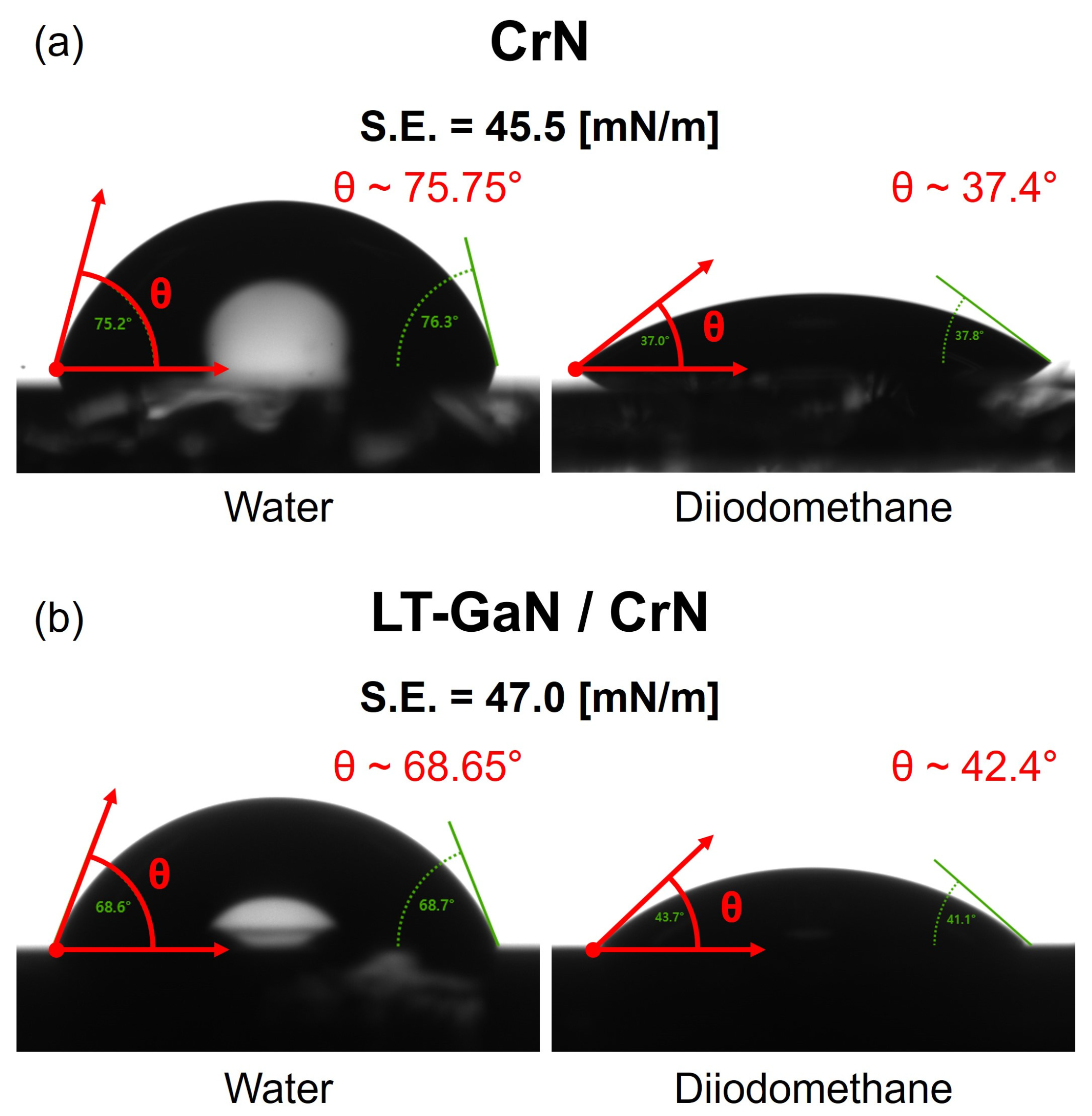
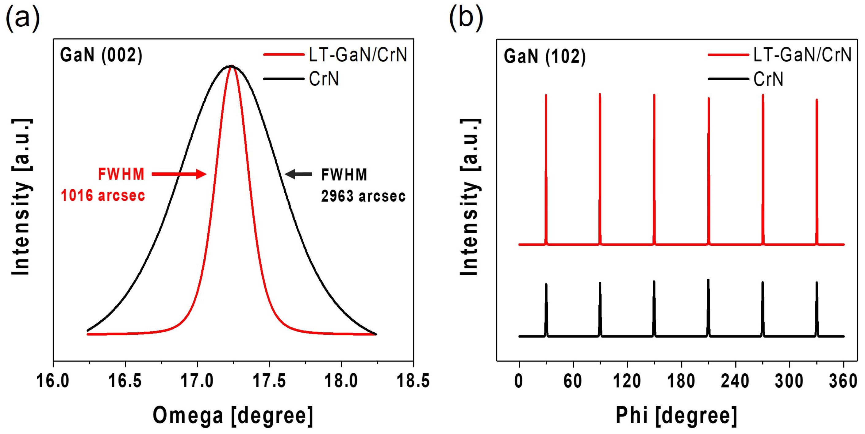
3. Results and Discussion
4. Conclusions
Author Contributions
Funding
Institutional Review Board Statement
Informed Consent Statement
Data Availability Statement
Conflicts of Interest
Abbreviations
| GaN | gallium nitride |
| LED | light-emitting diode |
| MOCVD | metal–organic chemical vapor deposition |
| LT | low temperature |
| LLO | laser lift-off |
| CLO | chemical lift-off |
| RF | radio frequency |
| HT | high temperature |
| XRD | X-ray diffraction |
| EDX | energy-dispersive X-ray spectroscopy |
| FWHM | full-width at half maximum |
| AFM | atomic force microscopy |
| SEM | scanning electron microscopy |
| MFP | mean free path |
References
- Strite, S.; Morkoç, H. GaN, AlN, and InN: A Review. J. Vac. Sci. Technol. B: Microelectron. Nanometer Struct. Process. Meas. Phenom. 1992, 10, 1237–1266. [Google Scholar] [CrossRef]
- DenBaars, S.P.; Feezell, D.; Kelchner, K.; Pimputkar, S.; Pan, C.-C.; Yen, C.-C.; Tanaka, S.; Zhao, Y.; Pfaff, N.; Farrell, R.; et al. Development of Gallium-Nitride-Based Light-Emitting Diodes (LEDs) and Laser Diodes for Energy-Efficient Lighting and Displays. Acta Mater. 2013, 61, 945–951. [Google Scholar] [CrossRef]
- Nakamura, S.; Senoh, M.; Nagahama, S.; Iwasa, N.; Yamada, T.; Matsushita, T.; Kiyoku, H.; Sugimoto, Y.; Kozaki, T.; Umemoto, H.; et al. InGaN/GaN/AlGaN-Based Laser Diodes with Modulation-Doped Strained-Layer Superlattices Grown on an Epitaxially Laterally Overgrown GaN Substrate. Appl. Phys. Lett. 1998, 72, 211–213. [Google Scholar] [CrossRef]
- Cho, Y.S.; Koh, E.K.; Park, Y.J.; Kim, E.K.; Hwang, S.-M.; Leem, S.-J.; Byun, D. Effects of GaN Buffer Layer Thickness on Characteristics of GaN Epilayer. Korean J. Mater. Res. 2001, 11, 575–579. [Google Scholar]
- Nakamura, S.; Harada, Y.; Seno, M. Novel Metalorganic Chemical Vapor Deposition System for GaN Growth. Appl. Phys. Lett. 1991, 58, 2021–2023. [Google Scholar] [CrossRef]
- Brückner, P.; Habel, F.; Scholz, F. HVPE Growth of High Quality GaN Layers. Phys. Status Solidi (C) 2006, 3, 1471–1474. [Google Scholar] [CrossRef]
- Byun, D.; Kim, G.; Lim, D.; Lee, D.; Choi, I.-H.; Park, D.; Kum, D.-W. Optimization of the GaN-Buffer Growth on 6H-SiC(0001). Thin Solid Films 1996, 289, 256–260. [Google Scholar] [CrossRef]
- Nakamura, S. GaN Growth Using GaN Buffer Layer. Jpn. J. Appl. Phys. 1991, 30, 1705–1707. [Google Scholar] [CrossRef]
- Kang, B.H.; Lee, J.E.; Kim, D.-S.; Bae, S.; Jung, S.; Park, J.; Jhin, J.; Byun, D. Effect of Amorphous and Crystalline AlN Buffer Layers Deposited on Patterned Sapphire Substrate on GaN Film Quality. J Nanosci. Nanotechnol. 2016, 16, 11563–11568. [Google Scholar] [CrossRef]
- Amano, H.; Sawaki, N.; Akasaki, I.; Toyoda, Y. Metalorganic Vapor Phase Epitaxial Growth of a High Quality GaN Film Using an AlN Buffer Layer. Appl. Phys. Lett. 1986, 48, 353–355. [Google Scholar] [CrossRef]
- Fischer, A.; Kühne, H.; Richter, H. New Approach in Equilibrium Theory for Strained Layer Relaxation. Phys. Rev. Lett. 1994, 73, 2712–2715. [Google Scholar] [CrossRef] [PubMed]
- Lee, W.H.; Im, I.H.; Minegishi, T.; Hanada, T.; Cho, M.W.; Yao, T. Structural Properties of CrN Buffers for GaN Growth. J. Korean Phys. Soc. 2006, 49, 928–933. [Google Scholar]
- Park, J.S.; Minegishi, T.; Lee, S.H.; Im, I.H.; Park, S.H.; Hanada, T.; Goto, T.; Cho, M.W.; Yao, T.; Hong, S.K.; et al. Effects of Interfacial Layer Structures on Crystal Structural Properties of ZnO Films. J. Vac. Sci. Technol. A: Vac. Surf. Film. 2008, 26, 90–96. [Google Scholar] [CrossRef]
- Lee, W.; Lee, S.; Goto, H.; Ko, H.; Cho, M.; Yao, T. Novel Buffer Layer for the Growth of GaN on C-sapphire. Phys. Status Solidi (C) 2006, 3, 1388–1391. [Google Scholar] [CrossRef]
- Park, J.; Yao, T. Growth of N-Polar GaN Using a CrN Buffer Layer on (0001) Al2O3 via Plasma-Assisted Molecular Beam Epitaxy. Thin Solid Films 2013, 531, 88–92. [Google Scholar] [CrossRef]
- Li, G.; Wang, W.; Yang, W.; Lin, Y.; Wang, H.; Lin, Z.; Zhou, S. GaN-Based Light-Emitting Diodes on Various Substrates: A Critical Review. Rep. Prog. Phys. 2016, 79, 056501. [Google Scholar] [CrossRef]
- Liu, H.F.; Liu, W.; Chua, S.J. Epitaxial Growth and Chemical Lift-off of GaInN/GaN Heterostructures on c- and r-Sapphire Substrates Employing ZnO Sacrificial Templates. J. Vac. Sci. Technol. A Vac. Surf. Films 2010, 28, 590–594. [Google Scholar] [CrossRef]
- Kelly, M.K.; Ambacher, O.; Dahlheimer, B.; Groos, G.; Dimitrov, R.; Angerer, H.; Stutzmann, M. Optical Patterning of GaN Films. Appl. Phys. Lett. 1996, 69, 1749–1751. [Google Scholar] [CrossRef]
- Wong, W.S.; Sands, T.; Cheung, N.W.; Kneissl, M.; Bour, D.P.; Mei, P.; Romano, L.T.; Johnson, N.M. Fabrication of Thin-Film InGaN Light-Emitting Diode Membranes by Laser Lift-Off. Appl. Phys. Lett. 1999, 75, 1360–1362. [Google Scholar] [CrossRef]
- Wong, W.S.; Sands, T.; Cheung, N.W.; Kneissl, M.; Bour, D.P.; Mei, P.; Romano, L.T.; Johnson, N.M. In x Ga 1−x N Light Emitting Diodes on Si Substrates Fabricated by Pd–In Metal Bonding and Laser Lift-Off. Appl. Phys. Lett. 2000, 77, 2822–2824. [Google Scholar] [CrossRef]
- Wong, W.S.; Cho, Y.; Weber, E.R.; Sands, T.; Yu, K.M.; Krüger, J.; Wengrow, A.B.; Cheung, N.W. Structural and Optical Quality of GaN/Metal/Si Heterostructures Fabricated by Excimer Laser Lift-Off. Appl. Phys. Lett. 1999, 75, 1887–1889. [Google Scholar] [CrossRef]
- Wu, Y.S.; Cheng, J.-H.; Ouyanga, H. Effects of Laser Sources on the Reverse-Bias Leakages of Laser Lift-Off GaN-Based LEDs. ECS Trans. 2007, 6, 285–287. [Google Scholar] [CrossRef]
- Chen, W.H.; Kang, X.N.; Hu, X.D.; Lee, R.; Wang, Y.J.; Yu, T.J.; Yang, Z.J.; Zhang, G.Y.; Shan, L.; Liu, K.X.; et al. Study of the Structural Damage in the (0001) GaN Epilayer Processed by Laser Lift-off Techniques. Appl. Phys. Lett. 2007, 91, 121114. [Google Scholar] [CrossRef]
- Park, J.; Goto, T.; Yao, T.; Lee, S.; Cho, M. Local Stress Distribution in GaN Vertical Light-Emitting Diodes Fabricated Using CLO and LLO Methods. J. Phys. D Appl. Phys. 2013, 46, 155104. [Google Scholar] [CrossRef]
- Lin, C.-F.; Dai, J.-J.; Wang, G.-M.; Lin, M.-S. Chemical Lift-Off Process for Blue Light-Emitting Diodes. Appl. Phys. Express 2010, 3, 092101. [Google Scholar] [CrossRef]
- Jeong, W.S.; Ahn, M.J.; Ko, H.-A.; Shim, K.; Kang, S.; Kim, H.; Kim, D.; Jhin, J.; Byun, D. Fabrication Method of GaN Template for High-Speed Chemical Lift-Off. AIP Advances 2023, 13, 035316. [Google Scholar] [CrossRef]
- Ahn, M.; Shim, K.; Jeong, W.; Kang, S.; Kim, H.; Cho, S.; Byun, D. Effective Chemical Lift-Off for Air-Tunnel GaN on a Trapezoid-Patterned Sapphire Substrate. Micromachines 2023, 14, 753. [Google Scholar] [CrossRef]
- Lin, C.-F.; Dai, J.-J.; Lin, M.-S.; Chen, K.-T.; Huang, W.-C.; Lin, C.-M.; Jiang, R.-H.; Huang, Y.-C. An AlN Sacrificial Buffer Layer Inserted into the GaN/Patterned Sapphire Substrate for a Chemical Lift-Off Process. Appl. Phys. Express 2010, 3, 031001. [Google Scholar] [CrossRef]
- Horng, R.-H.; Hsueh, H.-H.; Ou, S.-L.; Tsai, C.-T.; Tsai, T.-Y.; Wuu, D.-S. Chemical Lift-off Process for Nitride LEDs from an Eco-GaN Template Using an AlN/Strip-Patterned-SiO2 Sacrificial Layer: Chemical Lift-off Process for Nitride LEDs. Phys. Status Solidi A 2017, 214, 1600657. [Google Scholar] [CrossRef]
- Ha, J.-S.; Lee, H.-J.; Lee, S.W.; Lee, H.J.; Lee, S.H.; Goto, H.; Cho, M.W.; Yao, T.; Hong, S.-K.; Toba, R.; et al. Reduction of Dislocations in GaN Films on AlN/Sapphire Templates Using CrN Nanoislands. Appl. Phys. Lett. 2008, 92, 091906. [Google Scholar] [CrossRef]
- Goto, H.; Lee, S.W.; Lee, H.J.; Lee, H.; Ha, J.S.; Cho, M.W.; Yao, T. Chemical Lift-off of GaN Epitaxial Films Grown on C-sapphire Substrates with CrN Buffer Layers. Phys. Status Solidi (C) 2008, 5, 1659–1661. [Google Scholar] [CrossRef]
- Goto, H.; Lee, H.; Lee, S.; Cho, M.; Yao, T. Free-standing GaN Substrates Fabricated by a Combination of Substrate Fracturing and Chemical Lift-off. Phys. Status Solidi (C) 2011, 8, 2123–2126. [Google Scholar] [CrossRef]
- Ha, J.-S.; Lee, S.W.; Lee, H.-J.; Lee, H.-J.; Lee, S.H.; Goto, H.; Kato, T.; Fujii, K.; Cho, M.W.; Yao, T. The Fabrication of Vertical Light-Emitting Diodes Using Chemical Lift-Off Process. IEEE Photon. Technol. Lett. 2008, 20, 175–177. [Google Scholar] [CrossRef]
- Gharavi, M.A.; Kerdsongpanya, S.; Schmidt, S.; Eriksson, F.; Nong, N.V.; Lu, J.; Balke, B.; Fournier, D.; Belliard, L.; le Febvrier, A.; et al. Microstructure and Thermoelectric Properties of CrN and CrN/Cr2N Thin Films. J. Phys. D Appl. Phys. 2018, 51, 355302. [Google Scholar] [CrossRef]
- Gall, D.; Shin, C.-S.; Spila, T.; Odén, M.; Senna, M.J.H.; Greene, J.E.; Petrov, I. Growth of Single-Crystal CrN on MgO(001): Effects of Low-Energy Ion-Irradiation on Surface Morphological Evolution and Physical Properties. J. Appl. Phys. 2002, 91, 3589–3597. [Google Scholar] [CrossRef]
- Lin, P.-C.; Tsai, Y.-T.; Gan, N.-H.; Yang, J.-R.; Wang, S.-H.; Chang, H.-Y.; Lin, T.-R.; Chiu, P.-K. Characteristics of Flakes Stacked Cr2N with Many Domains in Super Duplex Stainless Steel. Crystals 2020, 10, 965. [Google Scholar] [CrossRef]
- Liu, H.Y.; Tang, G.S.; Zeng, F.; Pan, F. Influence of Sputtering Parameters on Structures and Residual Stress of AlN Films Deposited by DC Reactive Magnetron Sputtering at Room Temperature. J. Cryst. Growth 2013, 363, 80–85. [Google Scholar] [CrossRef]
- Asgary, S.; Vaghri, E.; Daemi, M.; Esmaili, P.; Ramezani, A.H.; Memon, S.; Hoseinzadeh, S. Magnetron Sputtering Technique for Analyzing the Influence of RF Sputtering Power on Microstructural Surface Morphology of Aluminum Thin Films Deposited on SiO2/Si Substrates. Appl. Phys. A 2021, 127, 1–7. [Google Scholar] [CrossRef]
- Floro, J.A.; Hearne, S.J.; Hunter, J.A.; Kotula, P.; Chason, E.; Seel, S.C.; Thompson, C.V. The Dynamic Competition between Stress Generation and Relaxation Mechanisms during Coalescence of Volmer–Weber Thin FIlms. J. Appl. Phys. 2001, 89, 4886–4897. [Google Scholar] [CrossRef]
- Itagaki, N.; Nakamura, Y.; Narishige, R.; Takeda, K.; Kamataki, K.; Koga, K.; Hori, H.; Shiratani, M. Growth of Single Crystalline Films on Lattice-Mismatched Substrates through 3D to 2D Mode Transition. Sci. Rep. 2020, 10, 4669. [Google Scholar] [CrossRef]
- Huang, W.-C.; Chu, C.-M.; Wong, Y.-Y.; Chen, K.-W.; Lin, Y.-K.; Wu, C.-H.; Lee, W.-I.; Chang, E.-Y. Investigations of GaN Growth on the Sapphire Substrate by MOCVD Method with Different AlN Buffer Deposition Temperatures. Mater. Sci. Semicond. Process. 2016, 45, 1–8. [Google Scholar] [CrossRef]
- Rosová, A.; Dobročka, E.; Eliáš, P.; Hasenöhrl, S.; Kučera, M.; Gucmann, F.; Kuzmík, J. In (Ga)N 3D Growth on GaN-Buffered On-Axis and Off-Axis (0001) Sapphire Substrates by MOCVD. Nanometerials 2022, 12, 3496. [Google Scholar] [CrossRef] [PubMed]
- Kozbial, A.; Li, Z.; Conaway, C.; McGinley, R.; Dhingra, S.; Vahdat, V.; Zhou, F.; D’Urso, B.; Liu, H.; Li, L. Study on the Surface Energy of Graphene by Contact Angle Measurements. Langmuir 2014, 30, 8598–8606. [Google Scholar] [CrossRef] [PubMed]
- Ahn, M.; Jeong, W.; Shim, K.; Kang, S.; Kim, H.; Kim, D.; Jhin, J.; Kim, J.; Byun, D. Selective-Area Growth Mechanism of GaN Microrods on a Plateau Patterned Substrate. Materials 2023, 16, 2462. [Google Scholar] [CrossRef]
- Smith, D.L.; Hoffman, D.W. Thin-Film Deposition: Principles and Practice. Phys. Today 1996, 49, 60–62. [Google Scholar] [CrossRef]

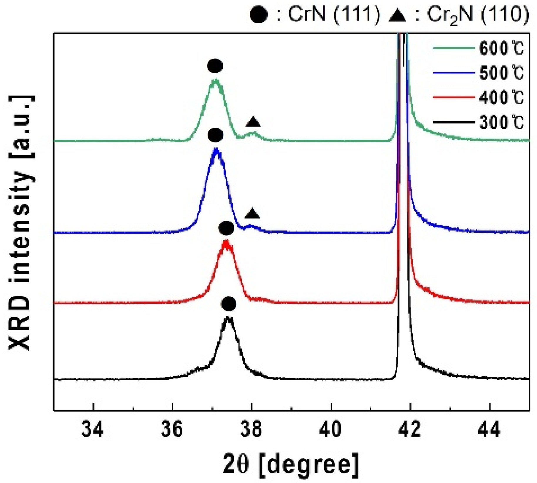
| Sample Code | 2θ (°) | d (Å) | a0 (Å) | Lattice Mismatch | |
|---|---|---|---|---|---|
| with Al2O3 (0001) (%) | with GaN (002) (%) | ||||
| CrN 300 °C | 37.402 | 2.402 | 4.161 | 7.11 | −7.73 |
| CrN 400 °C | 37.350 | 2.406 | 4.167 | 7.26 | −7.61 |
| CrN 500 °C | 37.104 | 2.421 | 4.193 | 7.94 | −7.02 |
| CrN 600 °C | 37.071 | 2.423 | 4.197 | 8.03 | −6.94 |
Disclaimer/Publisher’s Note: The statements, opinions and data contained in all publications are solely those of the individual author(s) and contributor(s) and not of MDPI and/or the editor(s). MDPI and/or the editor(s) disclaim responsibility for any injury to people or property resulting from any ideas, methods, instructions or products referred to in the content. |
© 2025 by the authors. Licensee MDPI, Basel, Switzerland. This article is an open access article distributed under the terms and conditions of the Creative Commons Attribution (CC BY) license (https://creativecommons.org/licenses/by/4.0/).
Share and Cite
Shim, K.-Y.; Kang, S.; Ahn, M.-J.; Cha, Y.; Ham, E.-G.; Kim, D.; Byun, D. Crystallographic Engineering of CrN Buffer Layers for GaN Thin Film Epitaxy. Materials 2025, 18, 1817. https://doi.org/10.3390/ma18081817
Shim K-Y, Kang S, Ahn M-J, Cha Y, Ham E-G, Kim D, Byun D. Crystallographic Engineering of CrN Buffer Layers for GaN Thin Film Epitaxy. Materials. 2025; 18(8):1817. https://doi.org/10.3390/ma18081817
Chicago/Turabian StyleShim, Kyu-Yeon, Seongho Kang, Min-Joo Ahn, Yukyeong Cha, Eojin-Gyere Ham, Dohoon Kim, and Dongjin Byun. 2025. "Crystallographic Engineering of CrN Buffer Layers for GaN Thin Film Epitaxy" Materials 18, no. 8: 1817. https://doi.org/10.3390/ma18081817
APA StyleShim, K.-Y., Kang, S., Ahn, M.-J., Cha, Y., Ham, E.-G., Kim, D., & Byun, D. (2025). Crystallographic Engineering of CrN Buffer Layers for GaN Thin Film Epitaxy. Materials, 18(8), 1817. https://doi.org/10.3390/ma18081817