Article

Investigation of the Etching Resistance of Yttrium Oxyfluoride Coating Deposited via Atmospheric Plasma Spraying Against Cl2/O2 Plasma

1
School of Materials Science and Engineering, Shanghai University, 333 Nanchen Road, Shanghai 200444, China
2
Shanghai Huali Integrated Circuit Corporation, 6 Liangteng Road, Pudong New Area, Shanghai 201314, China
3
Chongqing Genori Technology Co., Ltd., No. 66, Sendi Avenue, Xipeng Town, Jiulongpo District, Chongqing 401326, China
4
Zhejiang Institute of Advanced Materials, Shanghai University, Jiashan 314113, China
*
Author to whom correspondence should be addressed.
Materials 2025, 18(9), 1903; https://doi.org/10.3390/ma18091903
Submission received: 9 March 2025 / Revised: 14 April 2025 / Accepted: 17 April 2025 / Published: 23 April 2025

Abstract

:
Chlorine-based plasma is widely used in key etching applications. However, while etching the wafer materials, chlorine plasma can cause damage to the internal components of the etching chamber, which adversely affects the equipment’s lifespan. As a result, selecting appropriate coating materials for the chamber’s internal components is essential for mitigating corrosion. The etch resistance of these coatings directly impacts not only the quality of wafer production but also the operational safety and maintenance cycle of the etching equipment. In this study, three yttrium oxyfluoride coatings with different oxygen contents (3%, 6%, and 9%) were prepared using atmospheric plasma spraying technology. The etch resistance of these YOF coatings, as well as yttrium oxide coating, was systematically investigated under a Cl2/O2 plasma environment. Transmission electron microscopy analysis revealed that at the initial stage, Cl formed a protective layer on the surface of the YOF coatings, effectively slowing down further etching by Cl. Among the samples, the YOF 6% coating exhibited the best etching resistance, which is primarily attributed to its higher capacity for Cl adsorption. Overall, YOF coatings demonstrated excellent resistance in chlorine-based plasma environments, with YOF 6% in particular showing great potential as an ideal protective material for etching chamber components.

1. Introduction

Modern computer chips are manufactured through a series of complex processes carried out on silicon wafers, involving the use of a wide range of advanced semiconductor equipment. For state-of-the-art chips, the number of processing steps can reach hundreds or even thousands of steps, covering material processing, metrology, visual inspection, and electrical testing [1,2,3,4,5]. To enhance chip performance and yield, these processes are meticulously co-optimized and, to a large extent, built upon the experience from previous technology nodes, thereby accelerating the time-to-market for advanced node products.
Plasma etching is a crucial process in semiconductor manufacturing [6,7,8]. In the semiconductor industry, plasmas containing active compounds such as fluorine and chlorine (e.g., CF4, C4F6, Cl2, HBr, SF6) are commonly used to etch silicon (Si), silicon dioxide (SiO2), and other materials [9]. The ion bombardment and reaction radiation from the plasma not only form the desired patterns on the wafer surface but also etch the chamber wall surfaces exposed to the plasma [10,11]. During the etching process, these gases react with the ceramic coating inside the chamber, leading to the corrosion of the etching machine components. The particles generated will contaminate the silicon wafer, fall onto its surface, and cause defects, significantly reducing the yield [12,13]. Therefore, the study of ceramic materials with high hardness, corrosion resistance, and chemical stability for covering the inner walls of the etching chamber is key to improving the yield of etching products [14,15,16,17,18].
Among the various plasma etching-resistant coating materials, ceramic materials are widely recognized for their low etching rate and low chemical reactivity, with yttrium oxide (Y2O3) being particularly notable [19,20,21,22,23]. Although yttrium oxide offers certain advantages as an etching-resistant material, it also has some drawbacks, such as its relatively weak resistance to fluorinated gases and lower chemical stability compared with other ceramic materials like YOF (e.g., the formation enthalpy of the metal–oxygen bond in YOF is 392 kJ·mol−1, lower than Y2O3’s 318 kJ·mol−1) [24,25]. In recent years, yttrium fluoride (YOF) has gained significant attention as an emerging etching-resistant ceramic coating material, due to its ability to effectively suppress chemical reactions with fluorinated gases such as CF4 and NF3 [26,27,28,29,30,31,32]. The atmospheric plasma spraying (APS) technique is commonly used to coat parts with ceramic materials like Y2O3 and YOF, due to its high spraying efficiency, dense coating structure, strong bond strength between the coating and substrate, wide availability of spraying materials, and low processing costs. By using the APS method, it is possible to quickly form the desired coating on the substrate by melting ceramic powders with particle sizes ranging from tens of microns to smaller sizes in a high-temperature plasma (10,000 K or higher).
The chlorine plasma, due to its mild reactions and moderate etching rate, enhances the controllability of the etching process, making it widely used in critical etching applications. However, previous studies on the etch resistance of YOF coatings have primarily focused on fluorine-based plasma environments [30,33], with limited research on the performance of YOF coatings in chlorine-based plasma environments [34]. This paper investigates the etching behavior of Y2O3 and YOF coatings deposited on Al2O3 substrates via atmospheric plasma spraying (APS) in Cl2/O2 plasma. The etch resistance of the coatings is evaluated by analyzing changes in their microstructure and chemical composition. The results show that the YOF coating produced from raw material with 6% oxygen content exhibits excellent etch resistance in Cl2 plasma. Further research reveals that the oxygen content in the YOF raw material plays a crucial role in modulating the etching behavior and defect chemistry of the YOF coatings. Additionally, this paper evaluates the potential of YOF coatings as protective coatings for etching chamber walls.

2. Experimental Materials and Methods

2.1. Experimental Materials

YOF powders purchased from Nippon Yttrium Co., Ltd. (Fukuoka, Japan) and Y2O3 ceramic powders purchased from Shin-etsu (Tokyo, Japan) were used as raw materials for preparing high-performance etch-resistant coatings. The coatings prepared from raw materials with different oxygen contents (oxygen mass fractions of 3%, 6%, and 9%) were labeled as YOF 3%, YOF 6%, and YOF 9%, respectively. Additionally, Y2O3 was used as a reference material. The deionized water used in the experiments was prepared in the laboratory, and ethanol, acetone, and other chemical reagents were purchased from Sinopharm without further purification.

2.2. Experimental Methods

The YOF series coatings and Y2O3 coatings were prepared using the Oerlikon Metco APS system from the Oerlikon Metco, New York, NY, USA. This APS system generates a high-temperature plasma jet by ionizing a mixture of argon and hydrogen gases, which melts the ceramic particles. The molten particles are then sprayed onto anodized aluminum substrates (50 mm × 50 mm × 3 mm). By precisely controlling the process parameters, coatings with a thickness of 200 µm were successfully formed on the metal substrates. To ensure the cleanliness of the aluminum alloy substrates, they were first sandblasted with SiO2 and then cleaned with acetone. To test the etching resistance of the coatings, the Kiyo EX inductively coupled plasma (ICP) etching machine from Lam Research was used in this study. The specific steps of the experiment are as follows: Cl2, O2, and He gases were introduced into the etching machine’s reaction chamber at flow rates of 200 standard cubic centimeters per minute (sccm), 10 sccm, and 15 sccm, respectively, while maintaining a constant pressure of 10 mTorr. The TCP RF power was set to 350 W, with an RF bias voltage of 250 V, and the plasma exposure time for the coating substrate was 300 h. To characterize the raw materials Y2O3 and YOF powders used for the coatings, field emission scanning electron microscopy (FE-SEM, SU8010, Hitachi, Tokyo, Japan) was employed. Cross-sectional, surface morphology, and microstructural analyses of the coating samples and the Cl2 plasma-etched samples were conducted using scanning electron microscopy (SEM5000, CIQTEK Co., Ltd., Hefei, China). Additionally, the phase composition of the raw materials and coatings was analyzed using X-ray diffraction (XRD, Rigaku Ultima IV, Tokyo, Japan; radiation source: Cu-K α ( λ = 1.5418 Å); scan range: 10–80 (2 θ ); scan rate: 2/min). The elemental composition of the coating surface was analyzed using X-ray photoelectron spectroscopy (XPS, K-Alpha, Thermo Scientific, Waltham, MA, USA, monochromatic Al-K α X-ray source, voltage 100 V, spot size 450 µm, energy 50 eV, detection angle 45). The crystal structure of the coatings was further examined using transmission electron microscopy (TEM). At the same time, the surface roughness of the coatings was measured using an atomic force microscope (AFM, Bruker Icon SCANASYST-6AIR, Billerica, MA, USA) to comprehensively evaluate the microstructure and surface characteristics of the coatings.

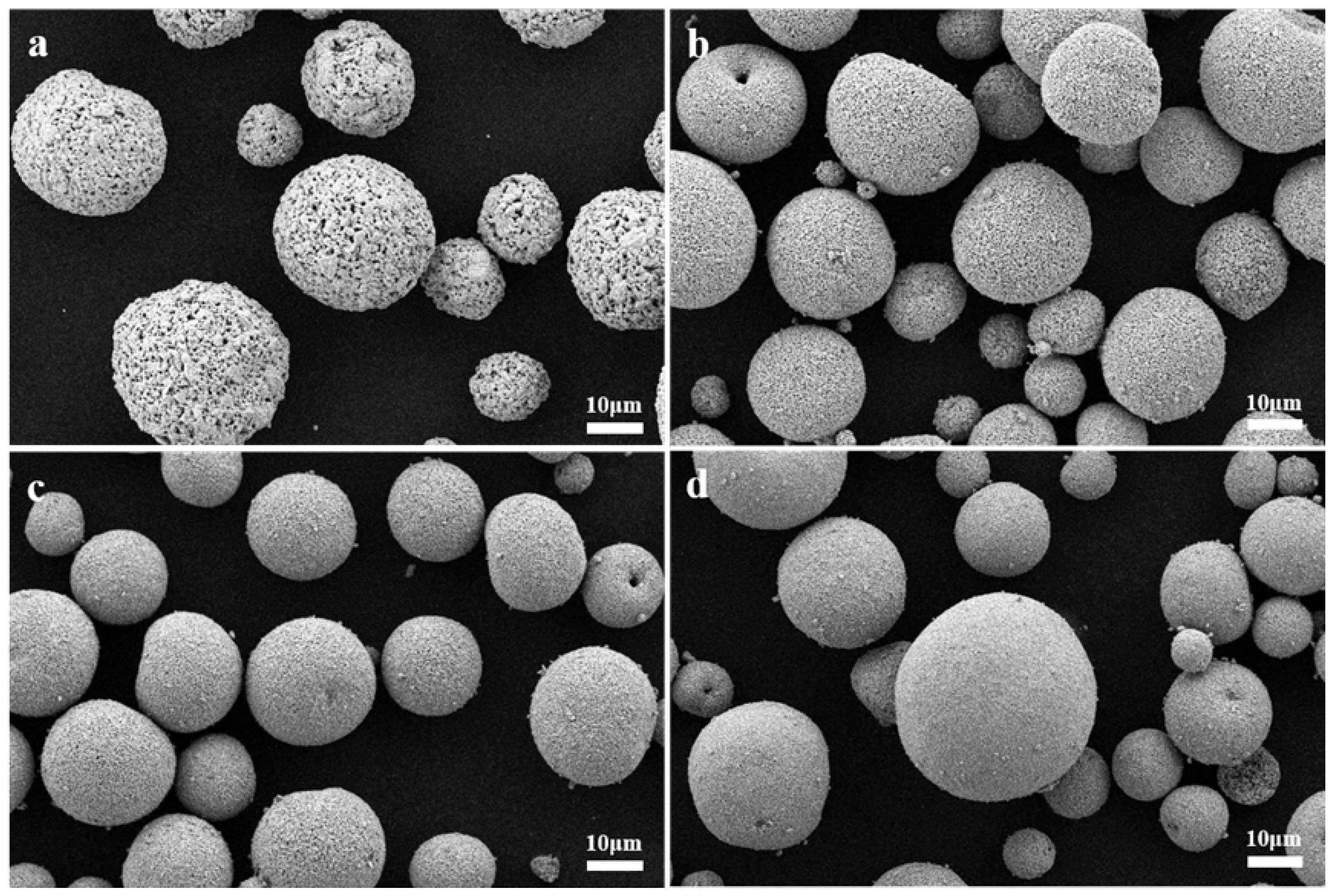
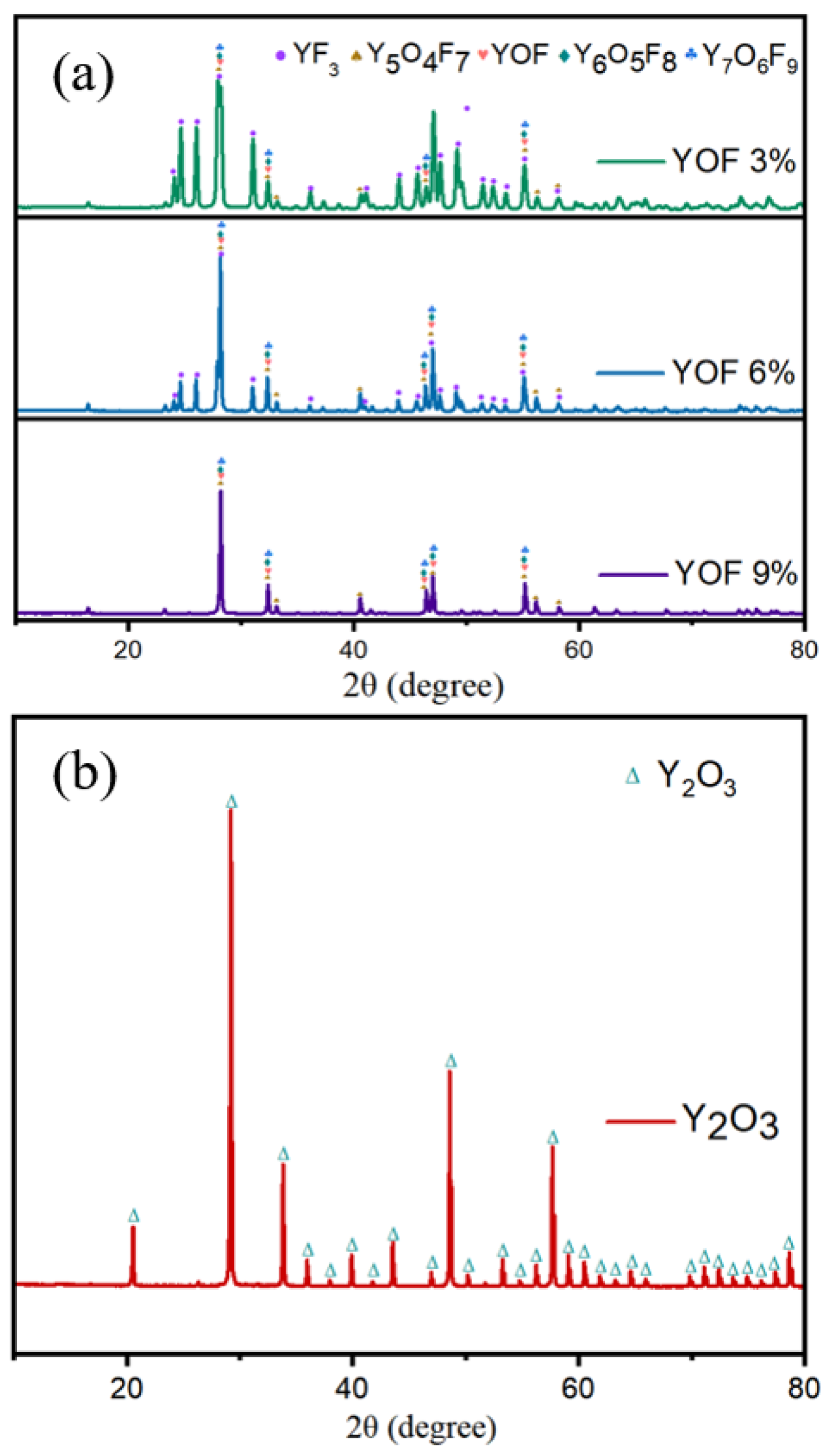
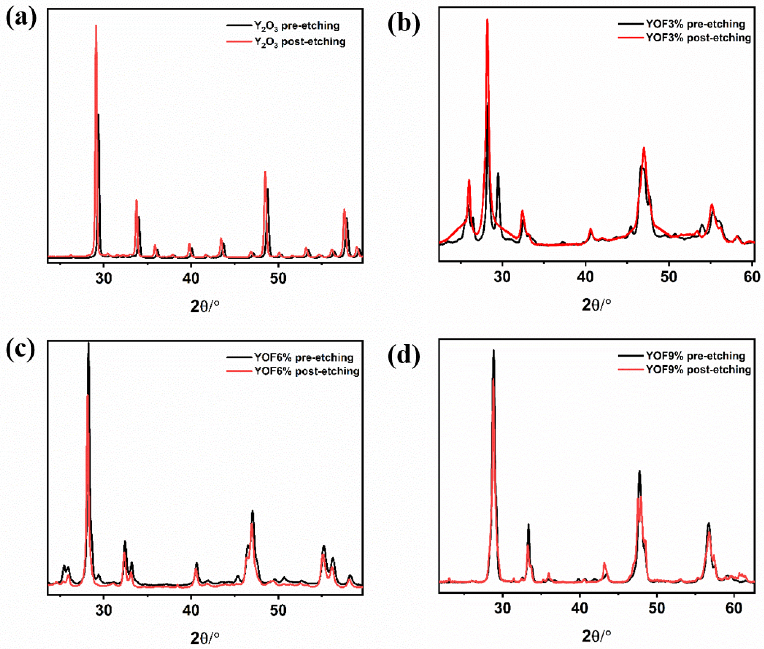
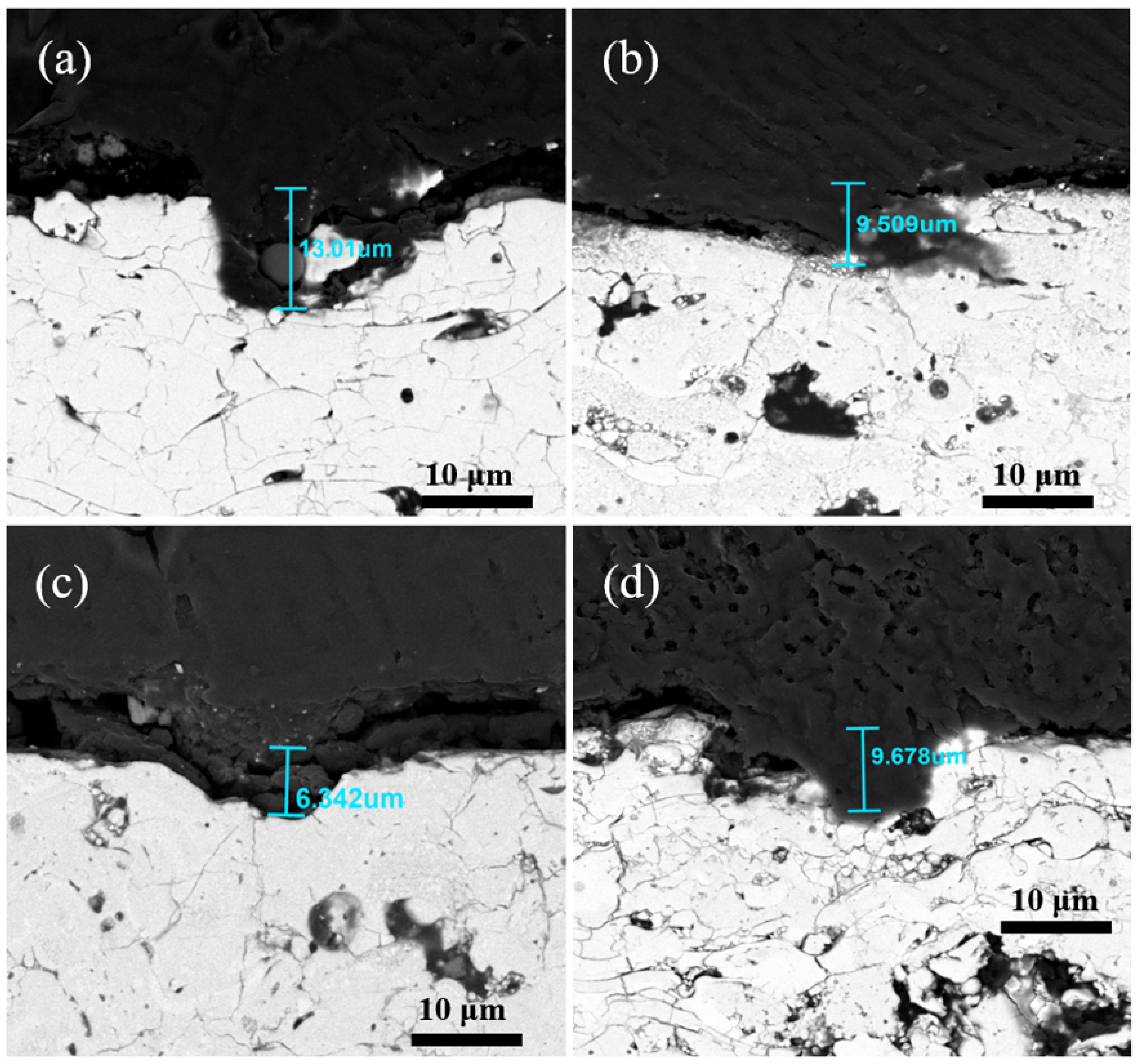
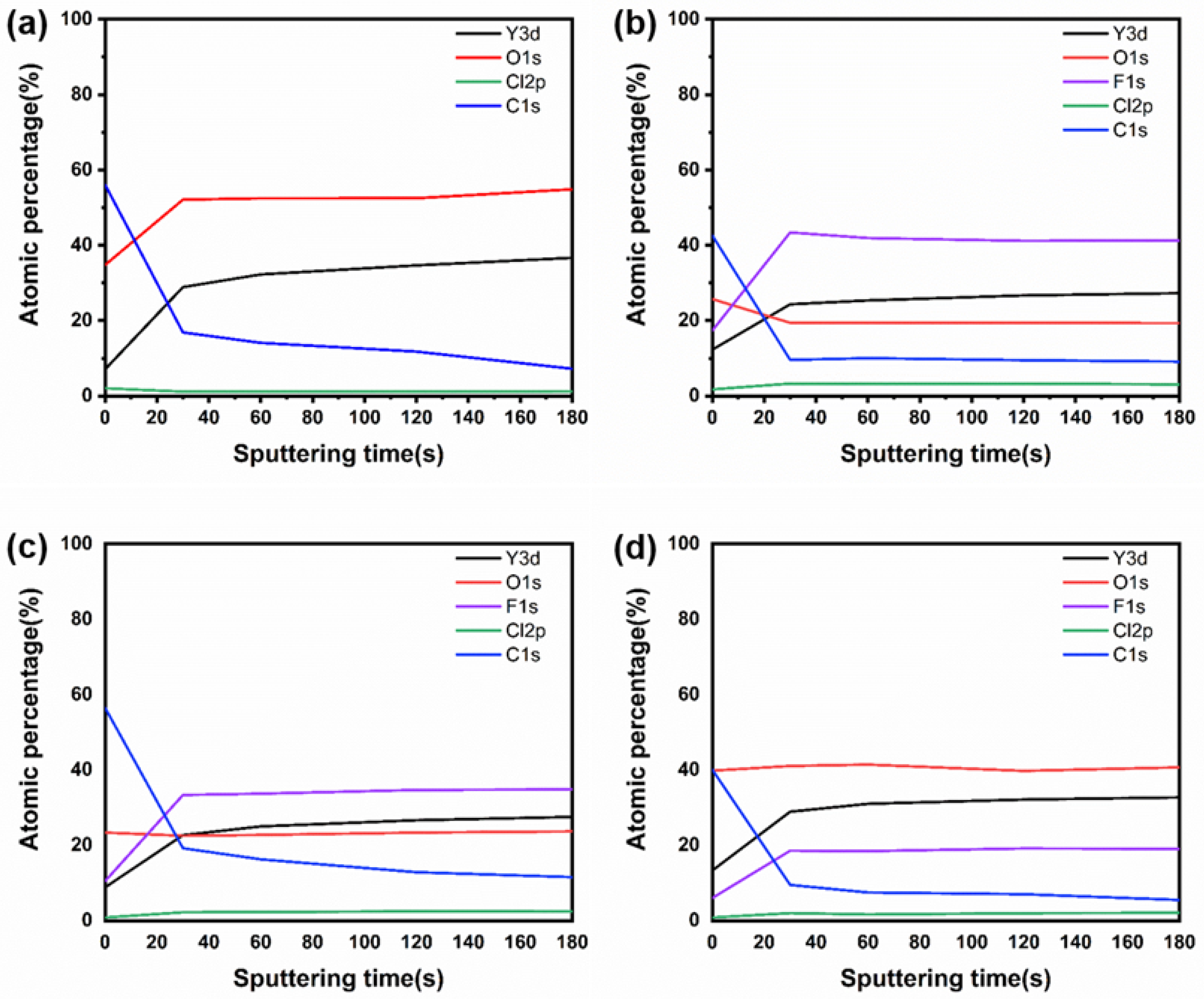
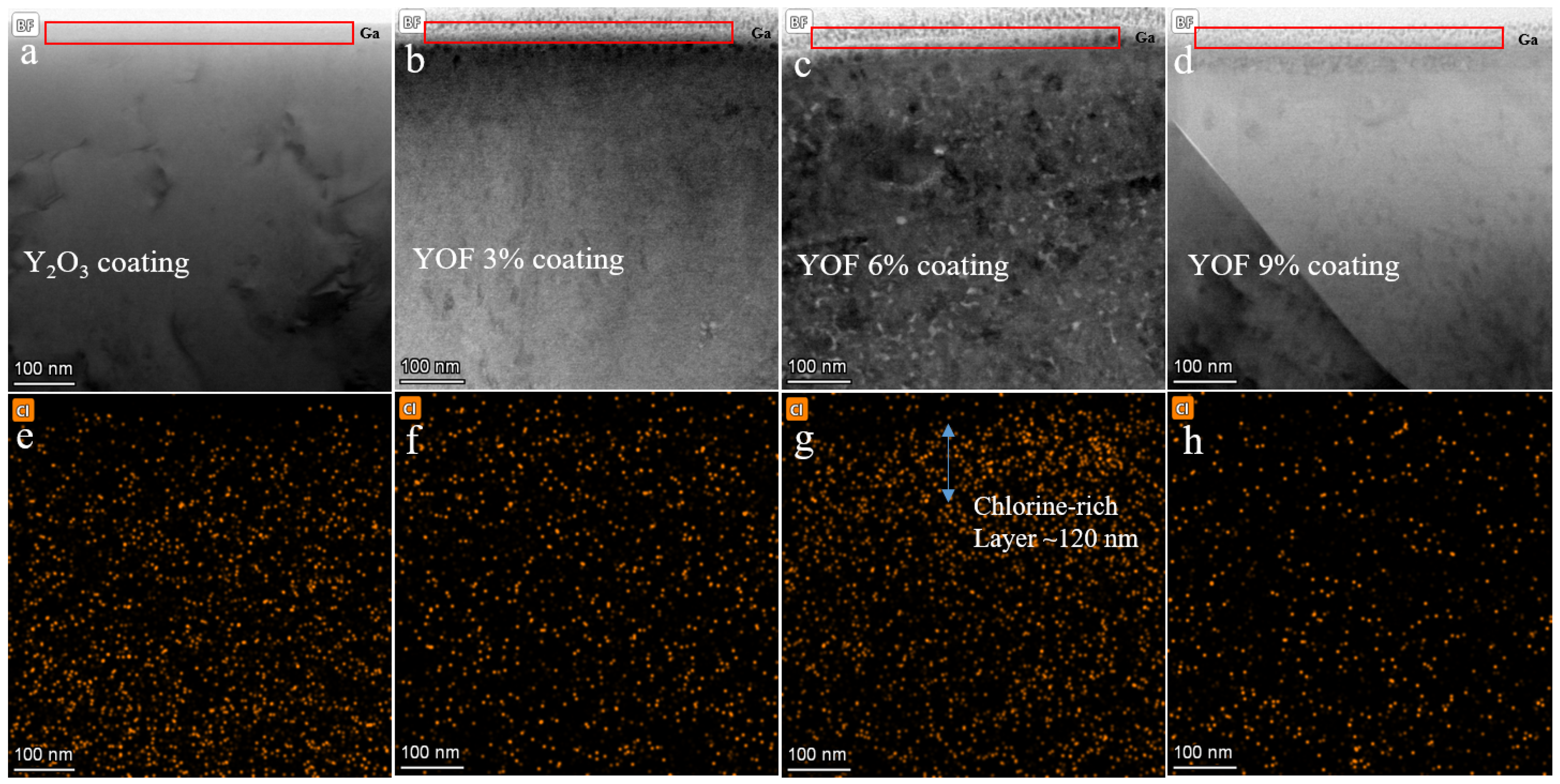
3. Discussion and Results

The Y2O3 and YOF powder raw materials were analyzed using scanning electron microscopy, and the results are shown in Figure 1. All of the raw materials consist of spherical particles. Particle size has an important impact on the spraying performance of the final coating, making it a key physical characteristic in the powder coating manufacturing process. Therefore, particle size and repose angle were further characterized using a particle size analyzer, with the results being shown in Table 1. The Y2O3 and YOF powders exhibit typical particle size distributions, with average particle sizes of 34.0 µm, 27.1 µm, 26.6 µm, and 27.7 µm and repose angles of 33.5, 33.7, 31.4, and 30.6, respectively. The spherical structure and limited particle size distribution of the raw material powders indicate that they are suitable for plasma spraying, providing good materials for the subsequent preparation of ceramic coatings through atmospheric plasma spraying.
The phase analysis of the raw materials was conducted using XRD, with the results being shown in Figure 2a. The analysis reveals that the XRD patterns of the YOF raw materials are consistent with the standard data for YOF (JCPDS No. 71-2100), Y2O3 (JCPDS No. 411105), and YF3 (JCPDS No. 74-0911). Additionally, the YOF powders are not composed of a single YOF phase, but rather a mixture of multiple YOF phases, such as Y5O4F7, Y6O5F8, and Y7O6F9. The YF3 peak is detectable in all YOF powders due to incomplete reactions, but its low concentration allows it to be considered negligible in terms of experimental impact. Figure 2b shows that the Y2O3 powder contains only the Y2O3 phase.
XRD was further used to characterize the phase composition of the coatings before and after etching, and the results are shown in Figure 3. The analysis indicates that after etching with chlorine plasma, the XRD diffraction peaks of all coatings shifted to the left. Taking the highest diffraction peak of each coating as an example, the diffraction peak of Y2O3 shifted from 29.38 to 29.12, YOF 3% shifted from 28.27 to 28.18, YOF 6% shifted from 28.24 to 28.14, and YOF 9% shifted from 28.84 to 28.78. According to the Bragg diffraction formula, the leftward shift of the diffraction peak indicates an increase in the lattice constant, which typically suggests a change in the atomic spacing within the lattice. In this study, the leftward shift of the diffraction peaks is primarily attributed to the high-energy Cl from the chlorine plasma bombarding the surface of the coatings during etching. Specifically, the radius of Cl is 0.181 nm, which is larger than that of F (0.133 nm) and O2− (0.14 nm). Therefore, during etching, Cl is likely to replace some of the F and O2− on the coating surface, leading to changes in the coating’s lattice structure and causing a shift of the diffraction peaks. This phenomenon further supports the idea that Cl interacts with the coating material during etching and affects its lattice structure.
Figure 4a–d show scanning electron microscope (SEM) images of the surface of Y2O3 and YOF coatings prepared by the atmospheric plasma spraying (APS) method. It can be observed that the surface morphology of all coatings consists of smooth and rough areas. The smooth areas are formed by molten particles that solidify on the substrate surface after being splattered and dispersed, while the rough areas are composed of particles that were not fully melted. These particles did not fully melt and bond with other particles, resulting in a rougher surface. To further observe the changes in the coating after chlorine plasma etching, the coatings were subjected to etching treatment, and the surface morphology after etching is shown in Figure 4e–h. By comparing the microscopic morphology before and after etching, it can be seen that both YOF series coatings and Y2O3 coatings underwent significant changes after chlorine plasma etching. Specifically, the YOF series coatings exhibited a more compact surface structure after etching, while the surface structure of the Y2O3 coating appeared more loose. This indicates that YOF coatings have better etching resistance compared with Y2O3 coatings.
Additionally, Figure 5 presents the changes in roughness of all coatings before and after etching, measured by atomic force microscopy (AFM). Before etching, the surface roughness of Y2O3, YOF 3%, YOF 6%, and YOF 9% coatings was 5.0 nm, 4.7 nm, 4.9 nm, and 6.2 nm, respectively; after etching, the roughness values increased to 19 nm, 18.5 nm, 18.6 nm, and 15.9 nm, respectively. This indicates that the surface roughness of the coatings increased after etching, which may be attributed to the bombardment of the coating surface by Cl2 plasma, leading to material loss and structural damage. It is worth noting that the surface roughness of Y2O3 coatings is higher than that of YOF coatings. This is likely due to the larger particle size of Y2O3 powder. During the APS coating process, larger particles are more difficult to fully melt, and unmelted particles impact the substrate and break apart, leading to more defects on the coating surface and thus increasing the surface roughness. Especially under the etching effect of chlorine plasma, the regions with unmelted particles are more prone to detachment, further exacerbating the increase in surface roughness of the coating.
This study carefully investigated the etching resistance of Y2O3, YOF 3%, YOF 6%, and YOF 9% coatings in chlorine plasma. During the testing process, a masking method was employed. A portion of the coating surface was masked to prevent this area from being affected by the chlorine plasma during etching. The masked region of the coating surface remained unetched, while the unmasked region was exposed to the etching environment. By comparing the surface height difference between the masked and unmasked regions after etching, the etching resistance of the coatings was effectively evaluated. The etching depth was characterized using scanning electron microscopy (SEM). Figure 6 shows the surface height differences after etching for Y2O3, YOF 3%, YOF 6%, and YOF 9% coatings, which were 13.01 µm, 9.509 µm, 6.342 µm, and 9.678 µm, respectively. The results indicate that the etching depth of the YOF series coatings is generally smaller than that of the Y2O3 coating, suggesting that the YOF series coatings have better etching resistance than the Y2O3 coating. Among the YOF series coatings, the YOF 6% coating exhibited the shallowest etching depth, demonstrating the best etching resistance. Additionally, the etching performance of the coatings was further evaluated through mass change measurements. Table 2 shows the weight loss of the four coatings after etching. All coatings experienced some degree of weight reduction after etching, with the specific weight loss per unit area being as follows: 0.486 g/cm2 for Y2O3, 0.127 g/cm2 for YOF 3%, 0.018 g/cm2 for YOF 6%, and 0.117 g/cm2 for YOF 9%. It can be observed that the YOF 6% coating had the lowest weight loss per unit area, further confirming its superior resistance to chlorine plasma etching. Based on the above test results, the YOF 6% coating exhibited the best etching resistance, with the shallowest etching depth and the smallest weight loss compared with the other coatings. Therefore, the YOF 6% coating may offer stronger etching resistance in practical applications, especially in environments with high-intensity plasma exposure.
An XPS analysis was conducted to investigate the chemical composition changes of Y2O3, YOF 3%, YOF 6%, and YOF 9% coatings during the Cl2/O2 etching process (0–180 s), and the results are shown in Figure 7. Based on the test data, the elemental changes can be roughly divided into two distinct stages. In the first stage (the first 30 s of etching), there were significant changes in atomic concentrations. During this stage, the atomic percentage of oxygen in the Y2O3 coating increased sharply from 35% to 53%, and the atomic percentage of fluorine increased from 8% to 29%. For the YOF series coatings, the atomic percentage of fluorine also showed significant changes, with YOF 3%, YOF 6%, and YOF 9% coatings increasing from 18%, 10%, and 5% to 45%, 30%, and 19%, respectively. At the same time, the atomic percentage of oxygen in the YOF coatings decreased from 25%, 23%, and 39% to 19%, 21%, and 43%, respectively. These changes indicate that fluorine and oxygen underwent different dynamic changes during the etching process, with the fluorine content increasing significantly, while the oxygen content decreased. In the second stage (etching time from 30 to 180 s), the atomic concentration changes of all coatings slowed down. This indicates that, as etching time increased, the chemical reactions on the coating surface gradually stabilized. During this stage, the YOF 6% coating exhibited the least change, indicating that it was the most stable during the etching process. This may be due to the composition or structure of this coating having better etch resistance under the etching conditions. Furthermore, the study found that the experimental powder did not contain carbon, but during the coating preparation process, carbon was mainly infiltrated into the sample randomly from the atmosphere. During etching, most of the carbon underwent oxidation, forming gaseous CO and CO2, while a small portion of the carbon was deposited as polymeric residues on the coating surface. This phenomenon further suggests that the chemical changes on the coating surface during etching involved not only oxygen and fluorine but may also be influenced by carbon contamination.
Figure 8a–d show cross-sectional TEM images of YOF and Y2O3 films after surface irradiation with Cl2 plasma, while Figure 8e–h present cross-sectional EDS mapping images of the same films after Cl2 plasma irradiation. The red box in the figures indicates the Ga layer plated using the focused ion beam (FIB) method. Analysis of these images reveals significant differences in the distribution of the chlorine element across the coatings. In particular, as shown in Figure 8g, the chlorine element is most densely distributed on the surface of the YOF 6% coating, with most of it being concentrated on the upper surface, forming a chlorine-rich layer approximately 120 nm thick. This suggests that the improved etching resistance of the YOF 6% coating may be closely related to the accumulation of chlorine ions on its surface. Chlorine ions can replace oxygen and fluorine ions in the coating, forming a protective layer that effectively prevents further chlorine ion erosion. In contrast, the chlorine element concentration on the surfaces of the Y2O3, YOF 3%, and YOF 9% coatings after etching is relatively low, and the distribution of chlorine is less uniform compared with the YOF 6% coating. This makes it more difficult for these coatings to form an effective protective layer against chlorine ions, resulting in poorer etching resistance in Cl2 plasma environments. Overall, the YOF 6% coating, due to its unique chlorine ion accumulation characteristic, exhibits the best etching resistance, while the other coatings, with uneven or low chlorine distribution, show relatively poor etching resistance.

4. Conclusions

YOF coatings with different oxygen contents were prepared on aluminum substrates using APS technology, and Y2O3 coatings were prepared for comparison. The etching resistance of all coatings in the Cl2/O2 plasma etching process was investigated. X-ray diffraction (XRD) results showed that after plasma etching, the diffraction peaks of YOF coatings shifted significantly to the left, indicating a change in lattice constants. This suggests that chlorine ions replaced fluorine and oxygen ions in the coating during the etching process, resulting in changes to the lattice structure. Scanning electron microscope (SEM) observations revealed that, compared with Y2O3 coatings, YOF series coatings exhibited denser microstructures and lower surface roughness after etching, demonstrating the superior etching resistance of YOF coatings. Etching depth measurements showed that the 6% YOF coating had the shallowest etching depth, only 6.342 µm, and the smallest mass loss per unit area, only 0.018 g/cm2, indicating the best etching resistance of this coating. Transmission electron microscope-energy dispersive spectroscopy (TEM-EDS) results showed that chloride ions accumulated on the surface of YOF series coatings, forming a chloride-rich layer. Among all the coatings, the chloride-rich layer of the 6% YOF coating was the thickest, reaching about 120 nm. This result suggests that the accumulation of chloride ions on the coating surface forms a protective chloride-rich layer, which is crucial for enhancing the etching resistance of the 6% YOF coating. In conclusion, the 6% YOF coating exhibited superior etching resistance compared with Y2O3, 3% YOF, and 9% YOF coatings in the Cl2/O2 plasma etching process, mainly due to the formation of its chloride-rich layer. This study indicates that YOF coatings, particularly the 6% YOF coating, have the potential to serve as a protective barrier against damage during the Cl2/O2 plasma etching process.

Author Contributions

Conceptualization, Z.T.; Methodology, Y.L., B.W. and H.M.; Validation, X.J.; Formal analysis, Y.L., K.A., Y.W., J.X., H.C. and Y.S.; Investigation, Z.T., Y.L., K.A., X.J., Y.W., J.X., H.M., H.C. and Y.S.; Resources, B.W. and Y.S.; Writing—original draft, Z.T.; Writing—review & editing, Z.T. and L.W.; Project administration, L.W.; Funding acquisition, L.W. All authors have read and agreed to the published version of the manuscript.

Funding

This research was funded by National Key R & D Program of China (No. 2023YFA1608703).

Institutional Review Board Statement

Not applicable.

Informed Consent Statement

Not applicable.

Data Availability Statement

The original contributions presented in this study are included in the article. Further inquiries can be directed to the corresponding author.

Conflicts of Interest

Authors Zaifeng Tang, Yukun Lv, Kaiqu Ang, Yuwei Wang, Jin Xu and Hua Meng were employed by the company Shanghai Huali Integrated Circuit Corporation, authors Bing Wang, Xiaojun Jiang and Hongli Chen were employed by the company Chongqing Genori Technology Co., Ltd. The remaining authors declare that the research was conducted in the absence of any commercial or financial relationships that could be construed as a potential conflict of interest.

References

  1. Ryu, J.E.; Park, S.; Park, Y.; Ryu, S.W.; Hwang, K.; Jang, H.W. Technological breakthroughs in chip fabrication, transfer, and color conversion for high-performance micro-LED displays. Adv. Mater. 2023, 35, 2204947. [Google Scholar] [CrossRef] [PubMed]
  2. Xu, Z.; Han, X.; Wu, W.; Li, F.; Wang, R.; Lu, H.; Pan, C. Controlled on-chip fabrication of large-scale perovskite single crystal arrays for high-performance laser and photodetector integration. Light. Sci. Appl. 2023, 12, 67. [Google Scholar] [CrossRef] [PubMed]
  3. Jia, L.; Wu, J.; Zhang, Y.; Qu, Y.; Jia, B.; Chen, Z.; Moss, D.J. Fabrication technologies for the on-chip integration of 2D materials. Small Methods 2022, 6, 2101435. [Google Scholar] [CrossRef] [PubMed]
  4. Han, X.; Huang, M.; Wu, Z.; Gao, Y.; Xia, Y.; Yang, P.; Jiang, Z. Advances in high-performance MEMS pressure sensors: Design, fabrication, and packaging. Microsystems Nanoeng. 2023, 9, 156. [Google Scholar] [CrossRef]
  5. Xu, S.; Wang, J.; Shu, H.; Zhang, Z.; Yi, S.; Bai, B.; Zou, W. Optical coherent dot-product chip for sophisticated deep learning regression. Light. Sci. Appl. 2021, 10, 221. [Google Scholar] [CrossRef]
  6. Economou, D.J. Pulsed plasma etching for semiconductor manufacturing. J. Phys. Appl. Phys. 2014, 47, 303001. [Google Scholar] [CrossRef]
  7. Cardinaud, C.; Peignon, M.C.; Tessier, P.Y. Plasma etching: Principles, mechanisms, application to micro-and nano-technologies. Appl. Surf. Sci. 2000, 164, 72–83. [Google Scholar] [CrossRef]
  8. Kwon, H.; Kim, Y.; Park, H.; Lee, C. The importance of intimate inter-crystallite bonding for the plasma erosion resistance of vacuum kinetic sprayed Y2O3 coating. Surf. Coatings Technol. 2019, 374, 493–499. [Google Scholar] [CrossRef]
  9. Tezani, L.L.; Pessoa, R.S.; Maciel, H.S.; Petraconi, G. Chemistry studies of SF6/CF4, SF6/O2 and CF4/O2 gas phase during hollow cathode reactive ion etching plasma. Vacuum 2014, 106, 64–68. [Google Scholar] [CrossRef]
  10. Coburn, J.W.; Winters, H.F. Plasma etching—A discussion of mechanisms. J. Vac. Sci. Technol. 1979, 16, 391–403. [Google Scholar] [CrossRef]
  11. Lee, C.G.; Kanarik, K.J.; Gottscho, R.A. The grand challenges of plasma etching: A manufacturing perspective. J. Phys. Appl. Phys. 2014, 47, 273001. [Google Scholar] [CrossRef]
  12. Park, J.; Lee, K.; Lee, J.; Hwang, H.W.; Jeong, G.; Kim, K.Y.; Jeon, H. Improvement of yttrium oxyfluoride coating with modified precursor solution for laser-induced hydrothermal synthesis. Coatings 2022, 12, 740. [Google Scholar] [CrossRef]
  13. So, J.; Kim, M.; Kwon, H.; Maeng, S.; Choi, E.; Chung, C.W.; Yun, J.Y. Investigation of contamination particles generation and surface chemical reactions on Al2O3, Y2O3, and YF3 coatings in F-based plasma. Appl. Surf. Sci. 2023, 629, 157367. [Google Scholar] [CrossRef]
  14. Lim, K.Y.; Kim, Y.W.; Kim, K.J. Mechanical properties of electrically conductive silicon carbide ceramics. Ceram. Int. 2014, 40, 10577–10582. [Google Scholar] [CrossRef]
  15. Zou, B.; Khan, Z.S.; Gu, L.; Fan, X.; Huang, W.; Wang, Y.; Cao, X. Microstructure, oxidation protection and failure mechanism of Yb2SiO5/LaMgAl11O19 coating deposited on C/SiC composites by atmospheric plasma spraying. Corros. Sci. 2012, 62, 192–200. [Google Scholar] [CrossRef]
  16. Kreethi, R.; Hwang, Y.J.; Lee, H.Y.; Park, J.H.; Lee, K.A. Surface analysis of yttrium oxyfluoride deposited via air plasma spraying for Erosion resistance against NF3 plasma. J. Korean Ceram. Soc. 2024, 61, 63–70. [Google Scholar] [CrossRef]
  17. Kreethi, R.; Hwang, Y.J.; Lee, H.Y.; Park, J.H.; Lee, K.A. Stability and plasma etching behavior of yttrium-based coatings by air plasma spray process. Surf. Coatings Technol. 2023, 454, 129182. [Google Scholar] [CrossRef]
  18. Ku, C.M.; Cheng, S. Factor design for the oxide etching process to reduce edge particle contamination in capacitively coupled plasma etching equipment. Appl. Sci. 2022, 12, 5684. [Google Scholar] [CrossRef]
  19. Zhao, D.; Wang, C.; Chen, Y.; Wang, Y. Phase composition, structural, and plasma erosion properties of ceramic coating prepared by suspension plasma spraying. Int. J. Appl. Ceram. Technol. 2018, 15, 1388–1396. [Google Scholar] [CrossRef]
  20. Miwa, K.; Takada, N.; Sasaki, K. Fluorination mechanisms of Al2O3 and Y2O3 surfaces irradiated by high-density CF4/O2 and SF6/O2 plasmas. J. Vac. Sci. Technol. 2009, 27, 831–835. [Google Scholar] [CrossRef]
  21. Kim, D.M.; Lee, S.H.; Alexander, W.B.; Kim, K.B.; Oh, Y.S.; Lee, S.M. X-ray photoelectron spectroscopy study on the interaction of yttrium–aluminum oxide with fluorine-based plasma. J. Am. Ceram. Soc. 2011, 94, 3455–3459. [Google Scholar] [CrossRef]
  22. Qin, X.; Zhou, G.; Yang, H.; Wong, J.I.; Zhang, J.; Luo, D.; Tang, D. Fabrication and plasma resistance properties of transparent YAG ceramics. Ceram. Int. 2012, 38, 2529–2535. [Google Scholar] [CrossRef]
  23. Lim, K.S.; Jang, T.S.; Jeong, J.H.; Hong, S.H.; Jin, J. Effect of Interlayer on Flatness and Adhesion of Aerosol-Deposited Yttrium Oxide Coating. Materials 2024, 17, 3533. [Google Scholar] [CrossRef]
  24. Tsunoura, T.; Yoshida, K.; Yano, T.; Kishi, Y. Fabrication, characterization, and fluorine-plasma exposure behavior of dense yttrium oxyfluoride ceramics. Jpn. J. Appl. Phys. 2017, 56, 06HC02. [Google Scholar] [CrossRef]
  25. Shiba, Y.; Teramoto, A.; Goto, T.; Kishi, Y.; Shirai, Y.; Sugawa, S. Stable yttrium oxyfluoride used in plasma process chamber. J. Vac. Sci. Technol. 2017, 35, 2. [Google Scholar] [CrossRef]
  26. Lee, J.; Lee, S.; Han, H.N.; Kim, W.; Hwang, N.M. Yttrium oxyfluoride coatings deposited by suspension plasma spraying using coaxial feeding. Coatings 2020, 10, 481. [Google Scholar] [CrossRef]
  27. Lee, S.; Lee, J.; Kim, W.; Hwang, N.M. Plasma etching behavior of YOF coating deposited by suspension plasma spraying in inductively coupled CHF3/Ar plasma. Coatings 2020, 10, 1023. [Google Scholar] [CrossRef]
  28. Lin, T.K.; Wang, W.K.; Huang, S.Y.; Tasi, C.T.; Wuu, D.S. Comparison of erosion behavior and particle contamination in mass-production CF4/O2 plasma chambers using Y2O3 and YF3 protective coatings. Nanomaterials 2017, 7, 183. [Google Scholar] [CrossRef]
  29. Ma, T.; List, T.; Donnelly, V.M. Comparisons of NF3 plasma-cleaned Y2O3, YOF, and YF3 chamber coatings during silicon etching in Cl2 plasmas. J. Vac. Sci. Technol. 2018, 36, 3. [Google Scholar] [CrossRef]
  30. Tahara, R.; Tsunoura, T.; Yoshida, K.; Yano, T.; Kishi, Y. Fabrication of dense yttrium oxyfluoride ceramics by hot pressing and their mechanical, thermal, and electrical properties. Jpn. J. Appl. Phys. 2018, 57, 06JF04. [Google Scholar] [CrossRef]
  31. Miyashita, K.; Yoshida, K.; Yano, T.; Matsukura, K.; Kishi, Y. Corrosion behavior of yttrium oxyfluoride ceramics in HCl, HNO3 and HF solutions at room temperature. Jpn. J. Appl. Phys. 2020, 59, SJJB02. [Google Scholar] [CrossRef]
  32. Wang, W.K.; Lin, Y.X.; Xu, Y.J. Structural and fluorine plasma etching behavior of sputter-deposition yttrium fluoride film. Nanomaterials 2018, 8, 936. [Google Scholar] [CrossRef] [PubMed]
  33. Lin, T.K.; Wuu, D.S.; Huang, S.Y.; Wang, W.K. Preparation and characterization of sprayed-yttrium oxyfluoride corrosion protective coating for plasma process chambers. Coatings 2018, 8, 373. [Google Scholar] [CrossRef]
  34. Ma, T.; List, T.; Donnelly, V.M. Y2O3 wall interactions in Cl2 etching and NF3 cleaning plasmas. J. Vac. Sci. Technol. 2017, 35, 3. [Google Scholar] [CrossRef]
Figure 1. SEM images of (a) Y2O3, (b) YOF 3%, (c) YOF 6%, and (d) YOF 9% powders.
Materials 18 01903 g001
Figure 2. XRD patterns of (a) YOF powders and (b) Y2O3 powder.
Materials 18 01903 g002
Figure 3. XRD spectra of the (a) Y2O3 coatings as-deposited and after plasma etching, (b) YOF 3% coatings as-deposited and after plasma etching, (c) YOF 6% coatings as-deposited and after plasma etching, and (d) YOF 9% coatings as-deposited and after plasma etching.
Materials 18 01903 g003
Figure 4. SEM images of (a) Y2O3, (b) YOF 3%, (c) YOF 6%, and (d) YOF 9% coatings before etching, and SEM images of (e) Y2O3, (f) YOF 3%, (g) YOF 6%, and (h) YOF 9% coatings after etching.
Materials 18 01903 g004
Figure 5. Atomic force microscopy (AFM) images of (a) Y2O3 coating before etching, (b) YOF 3% coating before etching, (c) YOF 6% coating before etching, and (d) YOF 9% coating before etching; and AFM images of (a’) Y2O3 coating after etching, (b’) YOF 3% coating after etching, (c’) YOF 6% coating after etching, and (d’) YOF 9% coating after etching.
Materials 18 01903 g005
Figure 6. SEM images for the etching depth of (a) Y2O3, (b) YOF 3%, (c) YOF 6%, and (d) YOF 9% coatings.
Materials 18 01903 g006
Figure 7. Variations in chemical compositions measured with XPS with the sputtering time for (a) Y2O3 coating, (b) YOF 3% coating, (c) YOF 6% coating, and (d) YOF 9% coating after exposure to Cl2/O2 plasma.
Materials 18 01903 g007
Figure 8. The TEM cross-sectional images of the (a) Y2O3 coating, (b) YOF 3% coating, (c) YOF 6% coating, and the (d) YOF 9% coating and the TEM-EDS mappings of chlorine in the (e) Y2O3 coating, (f) YOF 3% coating, (g) YOF 6% coating, and the (h) YOF 9% coating. The red box area in the figure is the Ga layer plated using the focused ion beam (FIB) method.
Materials 18 01903 g008
Table 1. Parameters of Y2O3 and YOF series powders.
ParameterY2O3YOF 3%YOF 6%YOF 9%
Median particle size (D50, µm)34.027.126.627.7
Angle of repose ()33.533.731.430.6
Table 2. The mass variation of Y2O3,YOF 3%,YOF 6%, and YOF 9% coatings before and after etching.
Y2O3YOF 3%YOF 6%YOF 9%
Pre-etching (g)24.1925.3325.3825.32
Post-etching (g)23.7424.5425.1124.59
Mass variation (g)−0.45−0.79−0.27−0.73
Decrement (g/cm2)0.0460.1270.0180.117
Disclaimer/Publisher’s Note: The statements, opinions and data contained in all publications are solely those of the individual author(s) and contributor(s) and not of MDPI and/or the editor(s). MDPI and/or the editor(s) disclaim responsibility for any injury to people or property resulting from any ideas, methods, instructions or products referred to in the content.

