
Bimorph Dual-Electrode ScAlN PMUT with Two Terminal Connections

Abstract
:1. Introduction
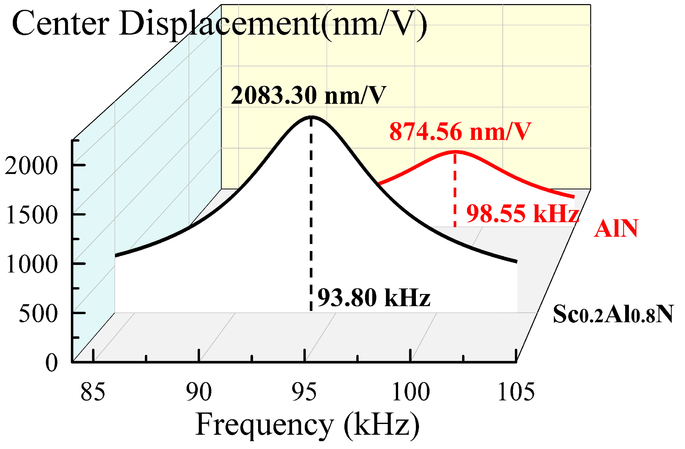
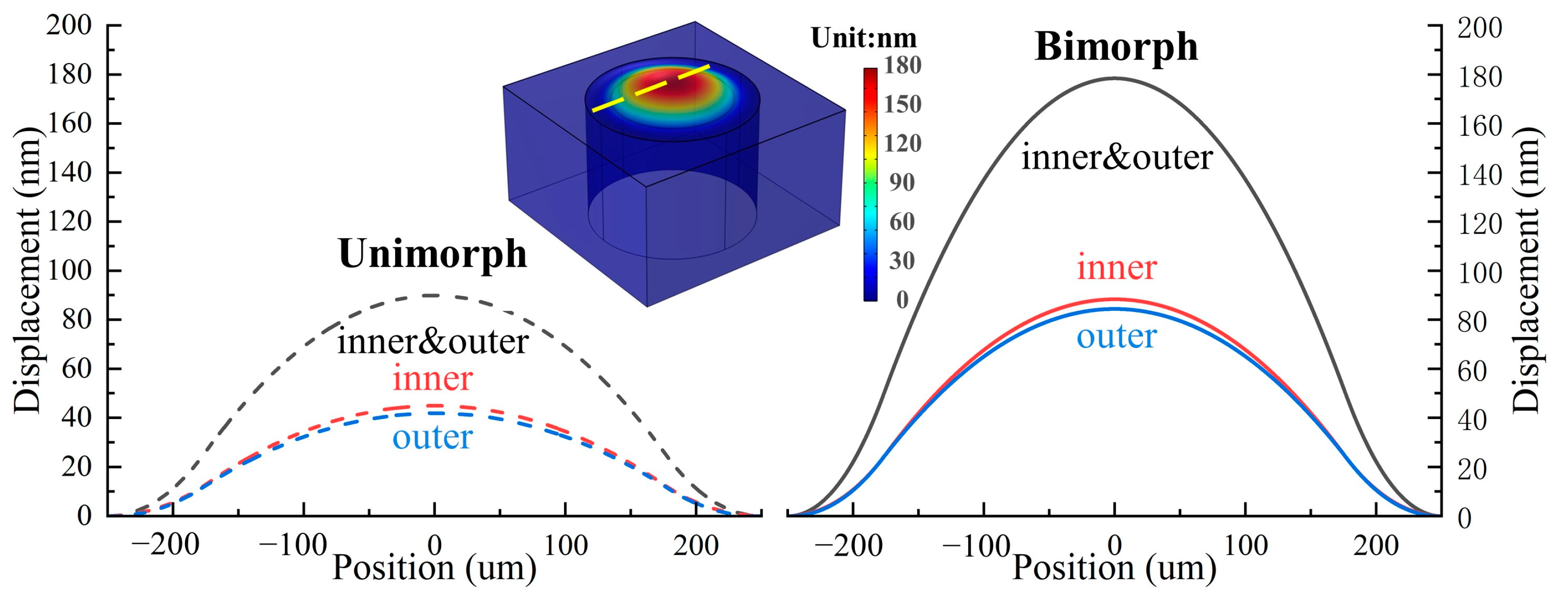
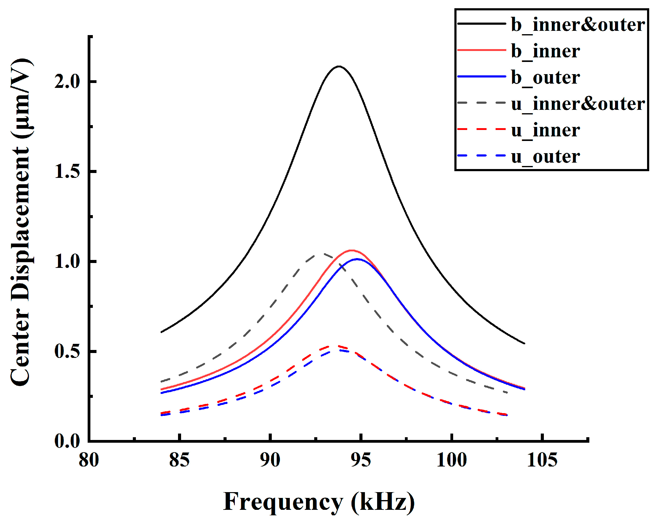
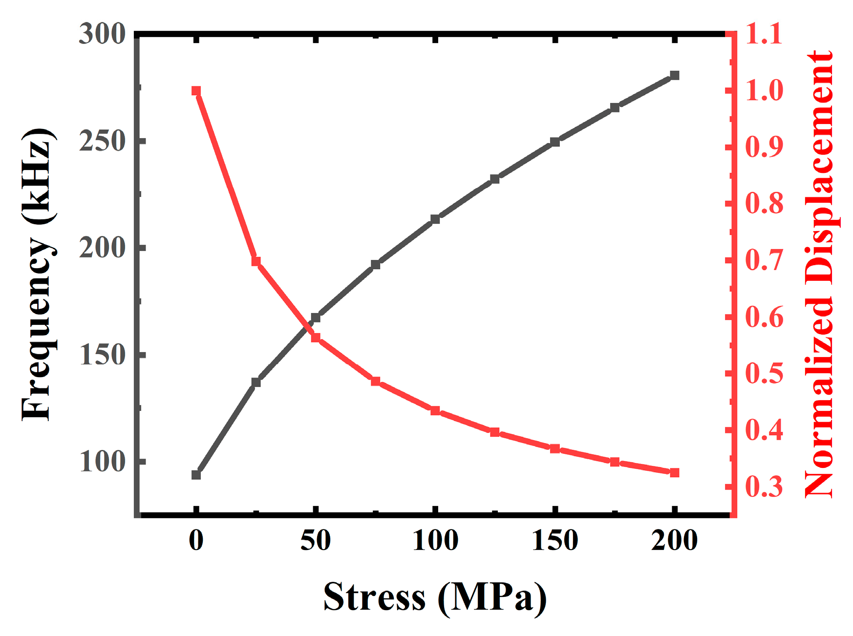
2. Design and Simulation
3. Fabrication
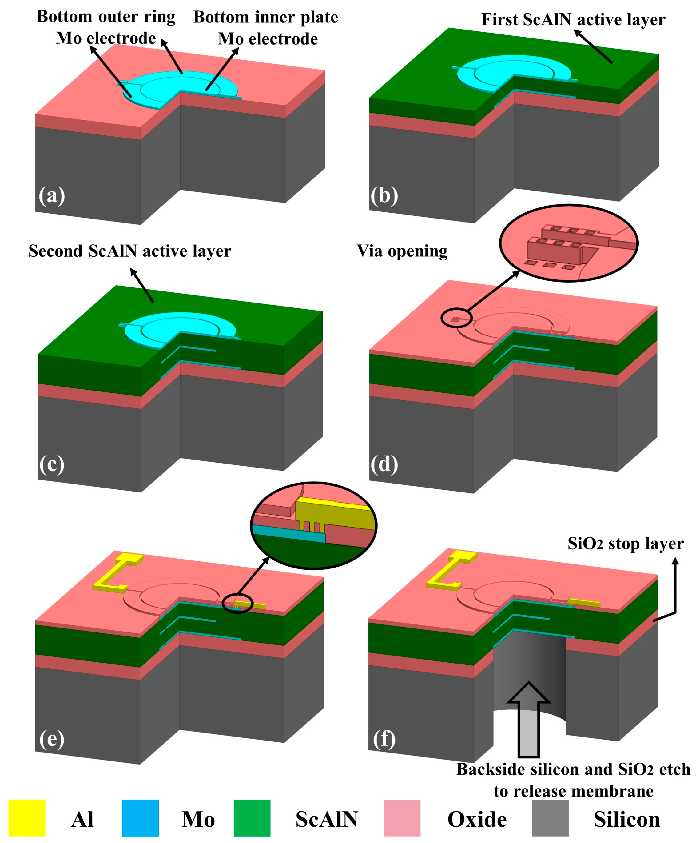
3.1. Process Flow
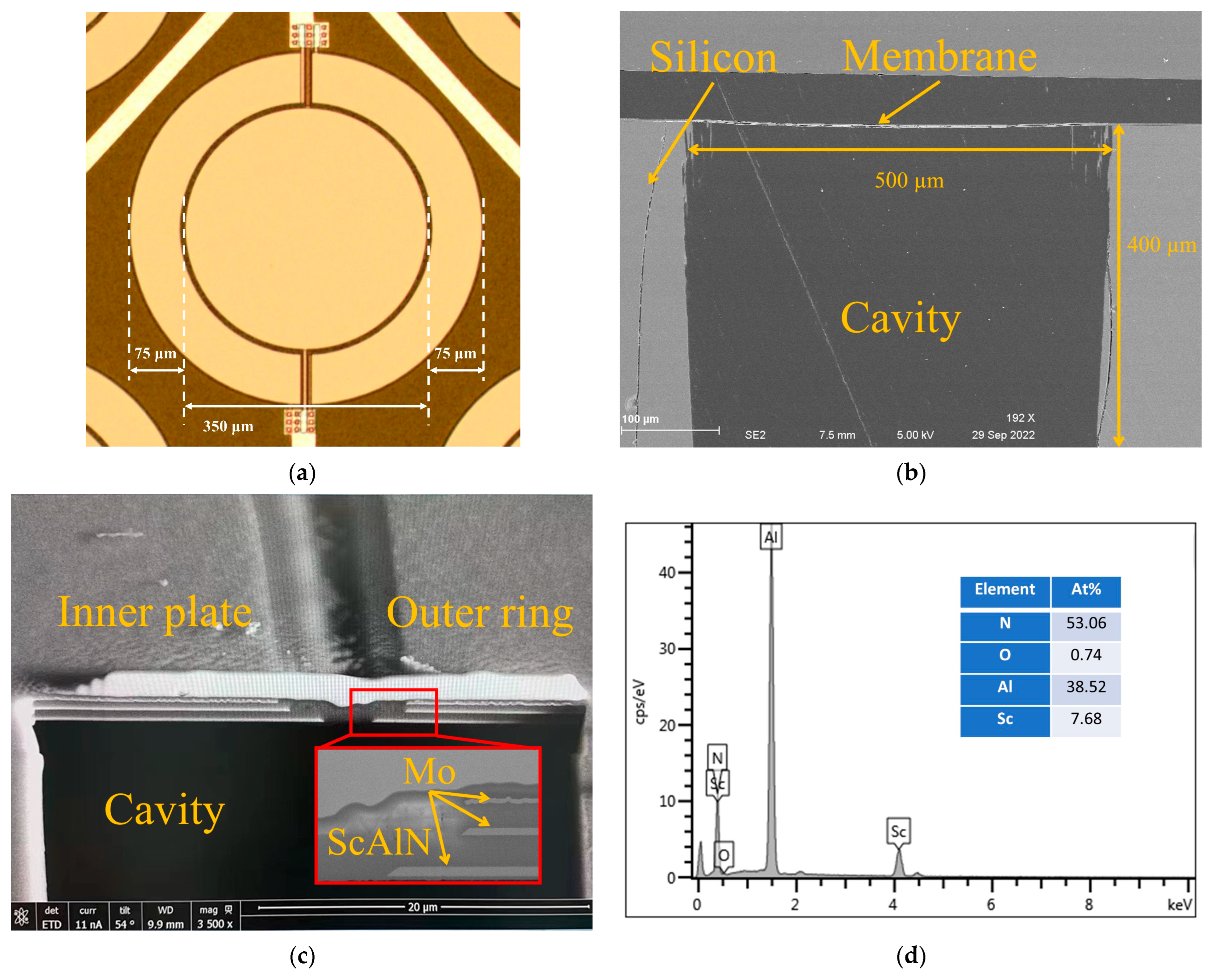
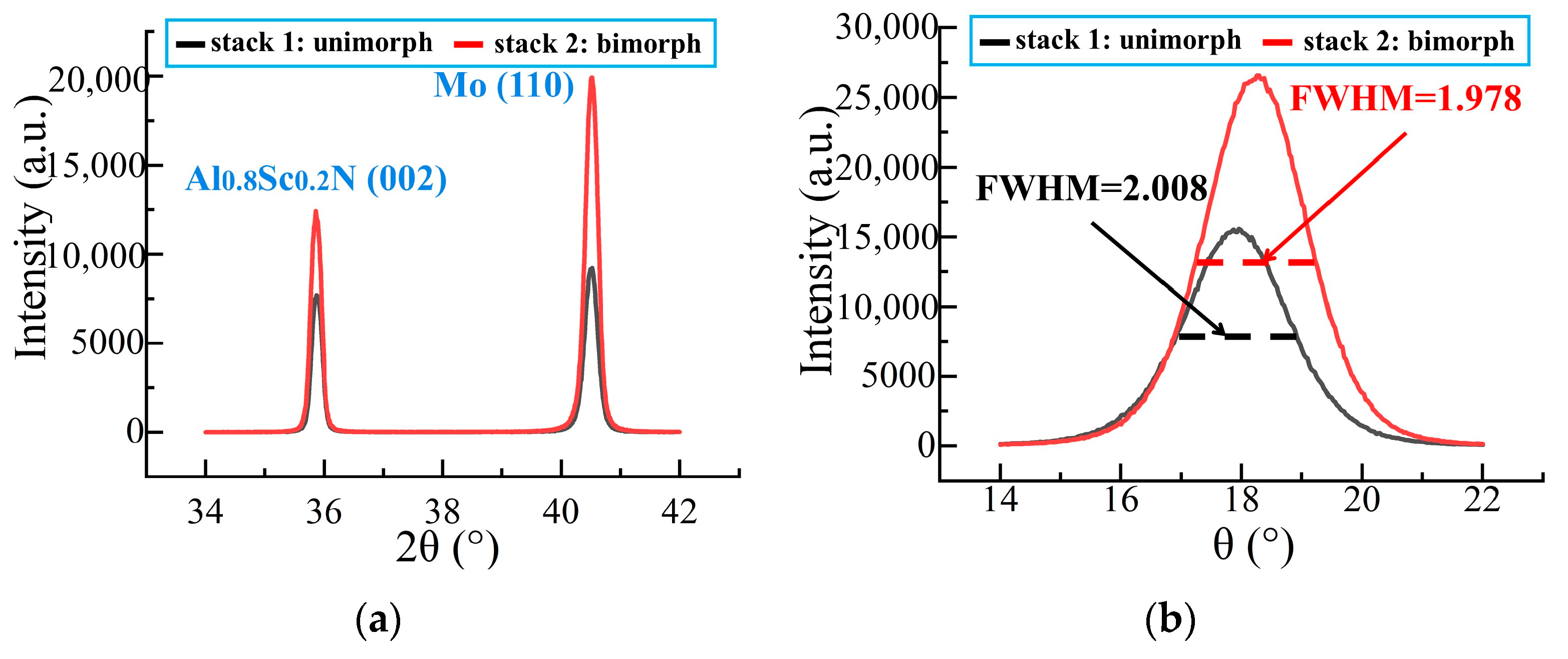
3.2. Fabrication Results
4. Experiment
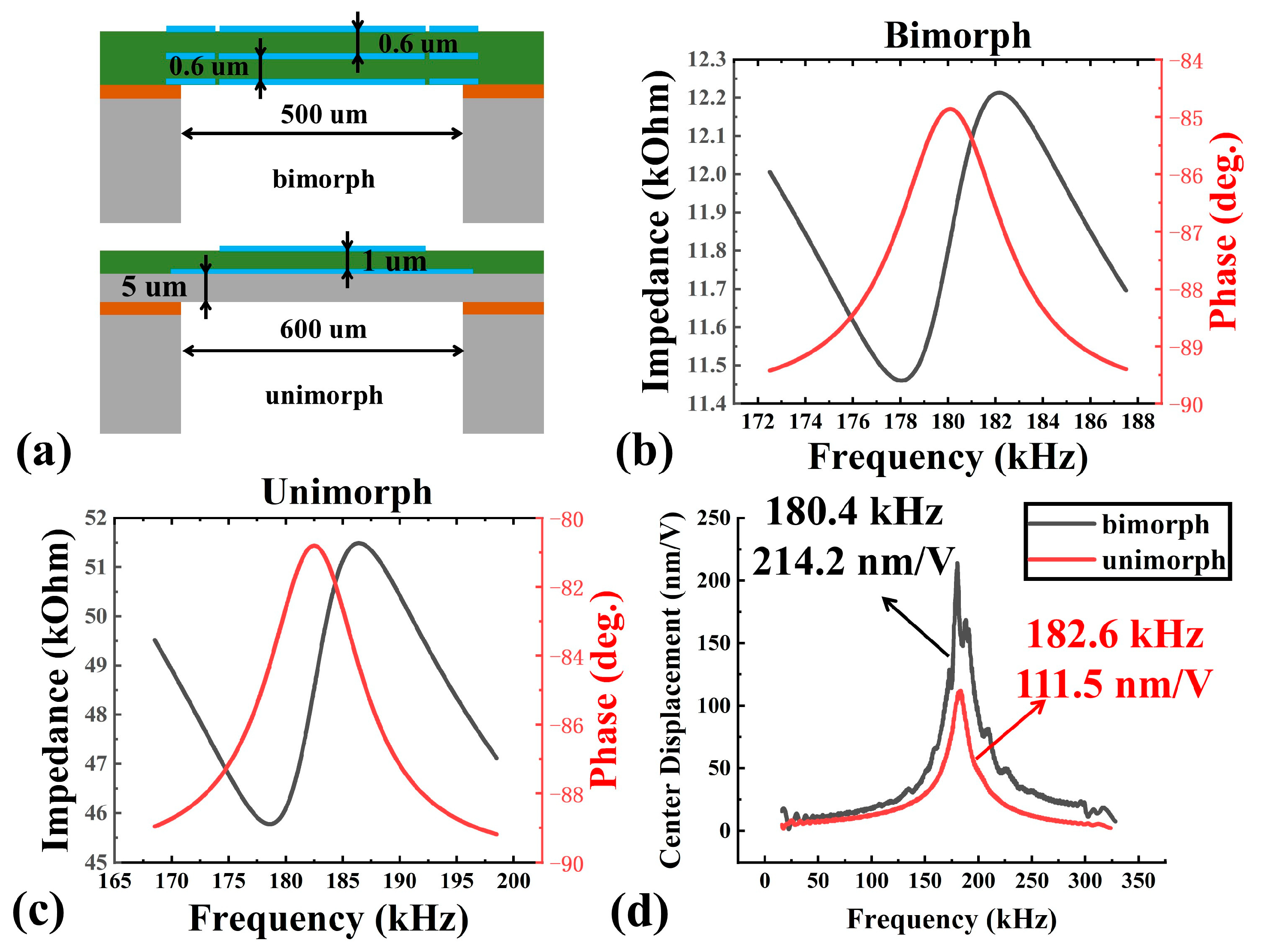
4.1. Dynamic Mechanical Displacement
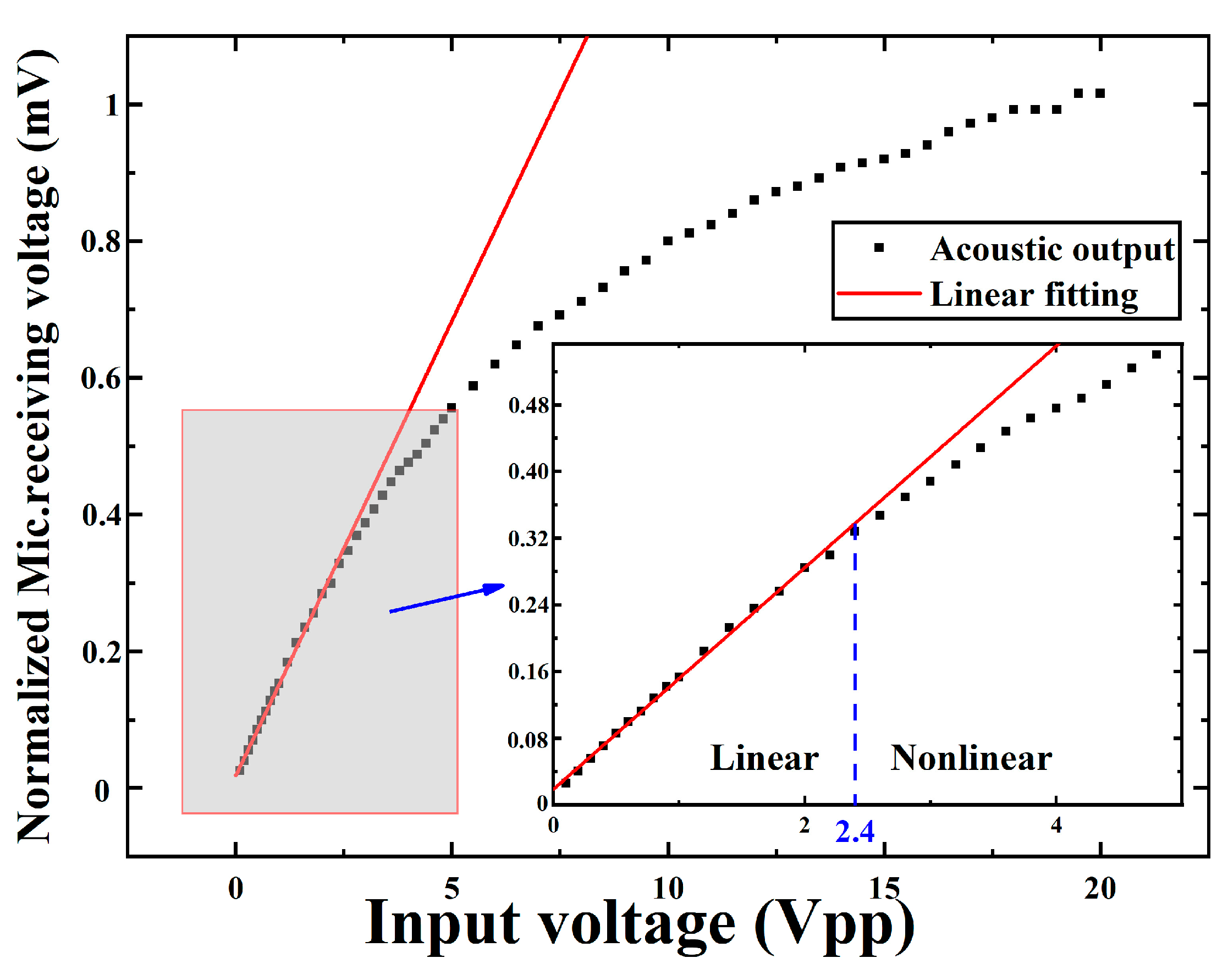
4.2. Transmitting Performance
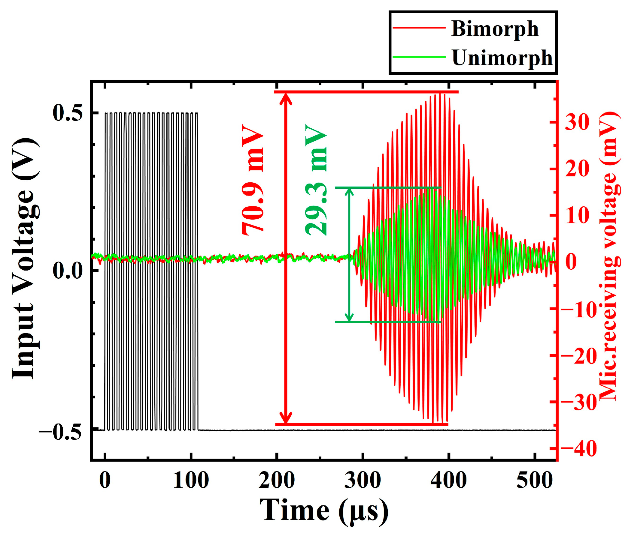
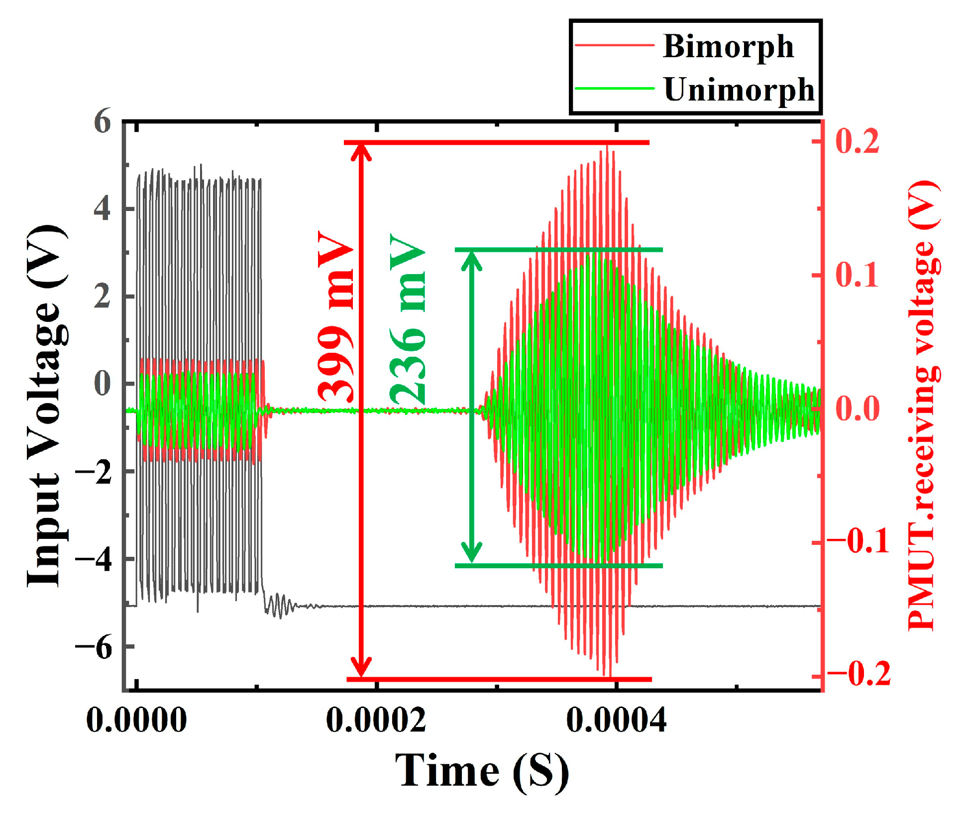
4.3. Receiving Performance
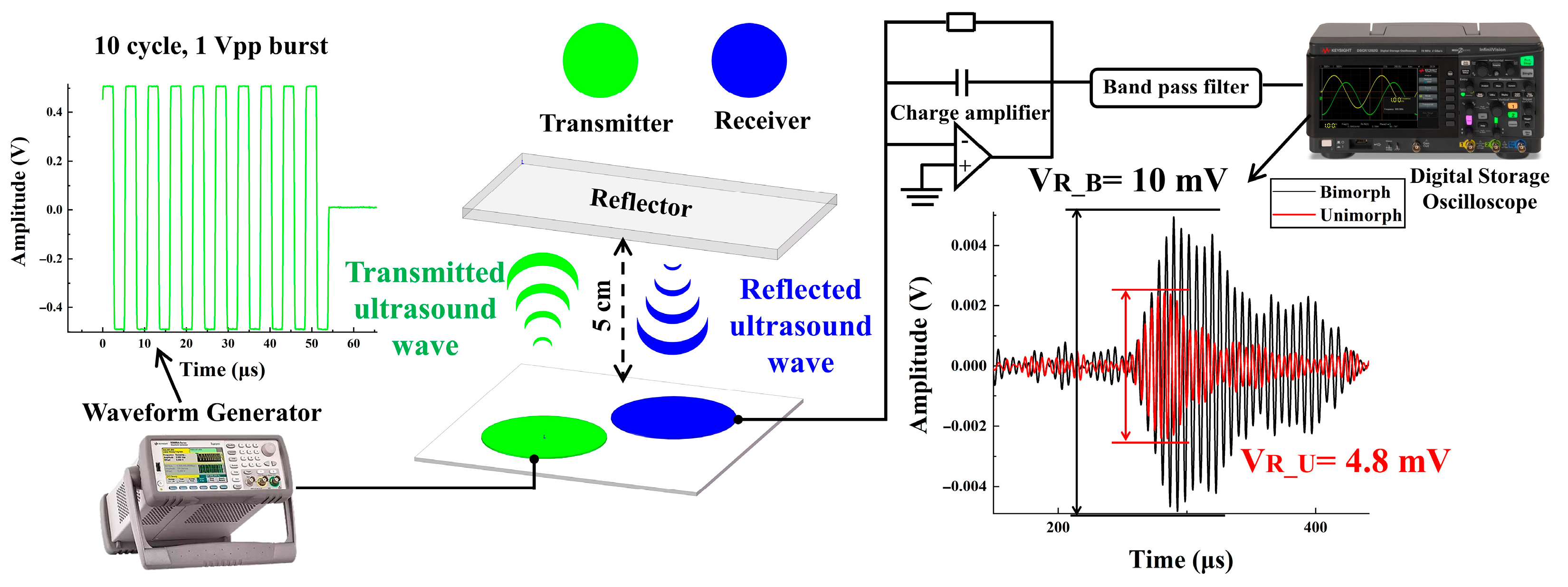
4.4. Pulse-Echo Experiments
5. Conclusions
Author Contributions
Funding
Data Availability Statement
Conflicts of Interest
References
- Qiu, Y.; Gigliotti, J.V.; Wallace, M.; Griggio, F.; Demore, C.E.M.; Cochran, S.; Trolier-McKinstry, S. Piezoelectric Micromachined Ultrasound Transducer (PMUT) Arrays for Integrated Sensing, Actuation and Imaging. Sensors 2015, 15, 8020–8041. [Google Scholar] [CrossRef] [PubMed] [Green Version]
- Przybyla, R.; Izyumin, I.; Kline, M.; Boser, B.; Shelton, S.; Guedes, A.; Horsley, D. An Ultrasonic Rangefinder Based on an ALN Piezoelectric Micromachined Ultrasound Transducer. In Proceedings of the SENSORS, 2010 IEEE, Waikoloa, HI, USA, 1–4 November 2010. [Google Scholar]
- Dausch, D.E.; Gilchrist, K.H.; Carlson, J.B.; Hall, S.D.; Castellucci, J.B.; Von Ramm, O.T. In Vivo Real-Time 3-D Intracardiac Echo Using PMUT Arrays. IEEE Trans. Ultrason. Ferroelectr. Freq. Control 2014, 61, 1754–1764. [Google Scholar] [CrossRef] [PubMed]
- Lu, Y.; Tang, H.; Fung, S.; Wang, Q.; Tsai, J.M.; Daneman, M.; Boser, B.E.; Horsley, D.A. Ultrasonic Fingerprint Sensor Using a Piezoelectric Micromachined Ultrasonic Transducer Array Integrated with Complementary Metal Oxide Semiconductor Electronics. Appl. Phys. Lett. 2015, 106, 263503. [Google Scholar] [CrossRef] [Green Version]
- Muralt, P.; Ledermann, N.; Paborowski, J.; Barzegar, A.; Gentil, S.; Belgacem, B.; Petitgrand, S.; Bosseboeuf, A.; Setter, N. Piezoelectric Micromachined Ultrasonic Transducers Based on PZT Thin Films. IEEE Trans. Ultrason. Ferroelectr. Freq. Control 2005, 52, 2276–2288. [Google Scholar] [CrossRef] [PubMed]
- Lu, Y.; Horsley, D.A. Modeling, Fabrication, and Characterization of Piezoelectric Micromachined Ultrasonic Transducer Arrays Based on Cavity SOI Wafers. J. Microelectrom. Syst. 2015, 24, 1142–1149. [Google Scholar] [CrossRef]
- Kusano, Y.; Luo, G.L.; Horsley, D.; Ishii, I.T.; Teshigahara, A. 36% Scandium-Doped Aluminum Nitride Piezoelectric Micromachined Ultrasonic Transducers. In Proceedings of the IEEE International Ultrasonics Symposium, IUS, Kobe, Japan, 22–25 October 2018. [Google Scholar]
- Wang, L.; Chen, S.; Zhang, J.; Zhou, J.; Yang, C.; Chen, Y.; Duan, H. High Performance 33.7 GHz Surface Acoustic Wave Nanotransducers Based on AlScN/Diamond/Si Layered Structures. Appl. Phys. Lett. 2018, 113, 093503. [Google Scholar] [CrossRef]
- Ji, Z.; Zhou, J.; Lin, H.; Wu, J.; Zhang, D.; Garner, S.; Gu, A.; Dong, S.; Fu, Y.Q.; Duan, H. Flexible Thin-Film Acoustic Wave Devices with off-Axis Bending Characteristics for Multisensing Applications. Microsyst. Nanoeng. 2021, 7, 1–9. [Google Scholar] [CrossRef] [PubMed]
- Zhou, J.; Ji, Z.; Guo, Y.; Liu, Y.; Zhuo, F.; Zheng, Y.; Duan, H. Strategy to minimize bending strain interference for flexible acoustic wave sensing platform. npj Flex. Electron. 2022, 6, 1–9. [Google Scholar] [CrossRef]
- Wang, Q.; Lu, Y.; Mishin, S.; Oshmyansky, Y.; Horsley, D.A. Design, Fabrication, and Characterization of Scandium Aluminum Nitride-Based Piezoelectric Micromachined Ultrasonic Transducers. J. Microelectrom. Syst. 2017, 26, 1132–1139. [Google Scholar] [CrossRef]
- Akhbari, S.; Sammoura, F.; Yang, C.; Heidari, A.; Horsley, D.; Lin, L. Self-Curved Diaphragms by Stress Engineering for Highly Responsive PMUT. In Proceedings of the IEEE International Conference on Micro Electro Mechanical Systems (MEMS), Estoril, Portugal, 18–22 January 2015. [Google Scholar]
- Wang, T.; Sawada, R.; Lee, C. A Piezoelectric Micromachined Ultrasonic Transducer Using Piston-like Membrane Motion. IEEE Electron Device Lett. 2015, 36, 957–959. [Google Scholar] [CrossRef]
- Akhbari, S.; Sammoura, F.; Yang, C.; Mahmoud, M.; Aqab, N.; Lin, L. Bimorph PMUT with Dual Electrodes. In Proceedings of the IEEE International Conference on Micro Electro Mechanical Systems (MEMS), Estoril, Portugal, 18–22 January 2015. [Google Scholar]
- Lou, L.; Yu, H.; Haw, M.T.X.; Zhang, S.; Gu, Y.A. Comparative Characterization of Bimorph and Unimorph AlN Piezoelectric Micro-Machined Ultrasonic Transducers. In Proceedings of the IEEE International Conference on Micro Electro Mechanical Systems (MEMS), Shanghai, China, 24–28 January 2016. [Google Scholar]
- Matloub, R.; Hadad, M.; Murait, P. Piezoelectric Coefficients of AlScN Thin Films in Comparison. In Proceedings of the 2016 IEEE International Frequency Control Symposium, IFCS 2016, New Orleans, LA, USA, 9–12 May 2016. [Google Scholar]
- Akiyama, M.; Kano, K.; Teshigahara, A. Influence of Growth Temperature and Scandium Concentration on Piezoelectric Response of Scandium Aluminum Nitride Alloy Thin Films. Appl. Phys. Lett. 2009, 95, 162107. [Google Scholar] [CrossRef]
- Sammoura, F.; Akhari, S.; Aqab, N.; Mahmoud, M.; Lin, L. Multiple Electrode Piezoelectric Micromachined Ultrasonic Transducers. In Proceedings of the IEEE International Ultrasonics Symposium, IUS, Chicago, IL USA, 3–6 September 2014. [Google Scholar]
- Cai, G.; Zhou, X.; Yi, Y.; Zhou, H.; Li, D.; Zhang, J.; Huang, H.; Mu, X. An Enhanced-Differential PMUT for Ultra-Long Distance Measurement in Air. In Proceedings of the IEEE International Conference on Micro Electro Mechanical Systems (MEMS), Gainesville, FL, USA, 25–29 January 2021. [Google Scholar]
- Lu, Y.; Wang, Q.; Horsley, D.A. Piezoelectric Micromachined Ultrasonic Transducers with Increased Coupling Coefficient via Series Transduction. In Proceedings of the 2015 IEEE International Ultrasonics Symposium, IUS 2015, Taipei, Taiwan, 21–24 October 2015. [Google Scholar]
- Iqbal, A.; Mohd-Yasin, F. Reactive Sputtering of Aluminum Nitride (002) Thin Films for Piezoelectric Applications: A Review. Sensors 2018, 18, 1797. [Google Scholar] [CrossRef] [PubMed] [Green Version]
- Xu, X.; Kuryatkov, V.; Borisov, B.; Pandikunta, M.; Nikishin, S.A.; Holtz, M. The Effect of BCl 3 Pretreatment on the Etching of AlN in Cl 2 -Based Plasma. MRS Proc. 2008, 1108. [Google Scholar] [CrossRef]
- Khan, F.A.; Zhou, L.; Kumar, V.; Adesida, I.; Okojie, R. High Rate Etching of AlN Using BCl3/Cl2/Ar Inductively Coupled Plasma. Mater. Sci. Eng. B Solid-State Mater. Adv. Technol. 2002, 95, 51–54. [Google Scholar] [CrossRef]
- Bliznetsov, V.; Johari, B.H.B.; Chentir, M.T.; Li, W.H.; Wong, L.Y.; Merugu, S.; Zhang, X.L.; Singh, N. Improving Aluminum Nitride Plasma Etch Process for MEMS Applications. J. Micromech. Microeng. 2013, 23, 117001. [Google Scholar] [CrossRef]
- Akhbari, S.; Sammoura, F.; Eovino, B.; Yang, C.; Lin, L. Bimorph Piezoelectric Micromachined Ultrasonic Transducers. J. Microelectrom. Syst. 2016, 25, 326–336. [Google Scholar] [CrossRef]
- Loebl, H.P.; Klee, M.; Metzmacher, C.; Brand, W.; Milsom, R.; Lok, P. Piezoelectric Thin AlN Films for Bulk Acoustic Wave (BAW) Resonators. Mater. Chem. Phys. 2003, 79, 143–146. [Google Scholar] [CrossRef]
- Luo, G.L.; Kusano, Y.; Horsley, D.A. Airborne Piezoelectric Micromachined Ultrasonic Transducers for Long-Range Detection. J. Microelectrom. Syst. 2021, 30, 81–89. [Google Scholar] [CrossRef]


| Material | E [Gpa] | ν | [kg/m3] | e31, f [C/m2] |
|---|---|---|---|---|
| AlN | 338 | 0.30 | 3230 | 1.05 |
| Sc0.2Al0.8N | 230 | 0.23 | 3520 | 1.6 |
Publisher’s Note: MDPI stays neutral with regard to jurisdictional claims in published maps and institutional affiliations. |
© 2022 by the authors. Licensee MDPI, Basel, Switzerland. This article is an open access article distributed under the terms and conditions of the Creative Commons Attribution (CC BY) license (https://creativecommons.org/licenses/by/4.0/).
Share and Cite
Ji, M.; Yang, H.; Zhou, Y.; Xiu, X.; Lv, H.; Zhang, S. Bimorph Dual-Electrode ScAlN PMUT with Two Terminal Connections. Micromachines 2022, 13, 2260. https://doi.org/10.3390/mi13122260
Ji M, Yang H, Zhou Y, Xiu X, Lv H, Zhang S. Bimorph Dual-Electrode ScAlN PMUT with Two Terminal Connections. Micromachines. 2022; 13(12):2260. https://doi.org/10.3390/mi13122260
Chicago/Turabian StyleJi, Meilin, Haolin Yang, Yongxin Zhou, Xueying Xiu, Haochen Lv, and Songsong Zhang. 2022. "Bimorph Dual-Electrode ScAlN PMUT with Two Terminal Connections" Micromachines 13, no. 12: 2260. https://doi.org/10.3390/mi13122260