Article

Vacuum Inner Spacer to Improve Annealing Effect during Electro-Thermal Annealing of Nanosheet FETs

School of Electronics Engineering, Chungbuk National University, Chungdae-ro 1, Cheongju 28644, Korea
*
Author to whom correspondence should be addressed.
Micromachines 2022, 13(7), 987; https://doi.org/10.3390/mi13070987
Submission received: 11 June 2022 / Revised: 21 June 2022 / Accepted: 23 June 2022 / Published: 24 June 2022
(This article belongs to the Special Issue Feature Papers of Micromachines in Engineering and Technology 2022)

Abstract

:
Electro-thermal annealing (ETA) in a MOSFET utilizes Joule heating. The high-temperature heat effectively cures gate dielectric damages induced by electrical stresses or ionizing radiation. However, even though ETA can be used to improve the reliability of logic and memory devices, applying ETA in state-of-the-art field-effect transistors (FETs) such as nanosheet FETs (NS FETs) has not yet been demonstrated. This paper addresses the heat distribution characteristic of an NS FET considering the application of ETA, using 3D simulations. A vacuum inner spacer is newly proposed to improve annealing effects during ETA. In addition, evaluations of the device scaling and annealing effect were performed with respect to gate length, nanosheet-to-nanosheet vertical space, and inner spacer thickness. Guidelines for ETA in NS FETs can be provided on the basis of the results.

1. Introduction

Semiconductor devices have been shrunk beyond Moore’s law, to increase output performance and to reduce power consumption [1]. However, as chip sizes become smaller, it is becoming more difficult to both control short-channel effects (SCEs) and improve device reliability. SCEs lead to increased standby power consumption by increasing off-state current (IOFF) [2]. SCEs have been suppressed by the evolution of device structures such as FinFETs [3] and gate-all-around (GAA) FETs [4]. It is also possible to improve immunity to SCEs with the aid of advanced material engineering and process technology [5].
In contrast to work on SCEs, there have been few breakthrough advances to address the degradation in reliability resulting from gate dielectric aging, except for lightly doped drain (LDD) and forming gas annealing (FGA), which were developed decades ago [6,7].
Recently, an electro-thermal annealing (ETA) configuration was introduced which utilizes Joule heat generated by the device itself to cure damaged gate dielectrics [8]. The ETA effectively cures the gate dielectric damage produced by hot-carrier injection (HCI), bias-temperature instability (BTI), and even total ionizing dose (TID). In addition, the ETA is applicable for removing contaminants such as photoresist (PR), moisture, or traps existing in channels [9,10]. However, additional power consumption is inevitably required to trigger the ETA.
Several approaches have been proposed to improve the annealing effect and to minimize the power consumption by modifying the device structure or materials [11,12]. However, these previous methods are not fully compatible with state-of-the-art logic transistors such as nanosheet FETs (NS FETs), since the backbone of the NS FET is completely different compared to conventional FinFETs and GAA FETs.
This paper demonstrates heat distribution characteristics during ETA in an NS FET. In addition, a novel device structure is provided which enables an improved annealing effect under identical power consumption. The proposed device structure contains a vacuum inner spacer which includes a vacuum dielectric. Device scaling was investigated in terms of gate module, multiple NS channels, and vacuum inner spacers, and the results are discussed for better use of ETA.

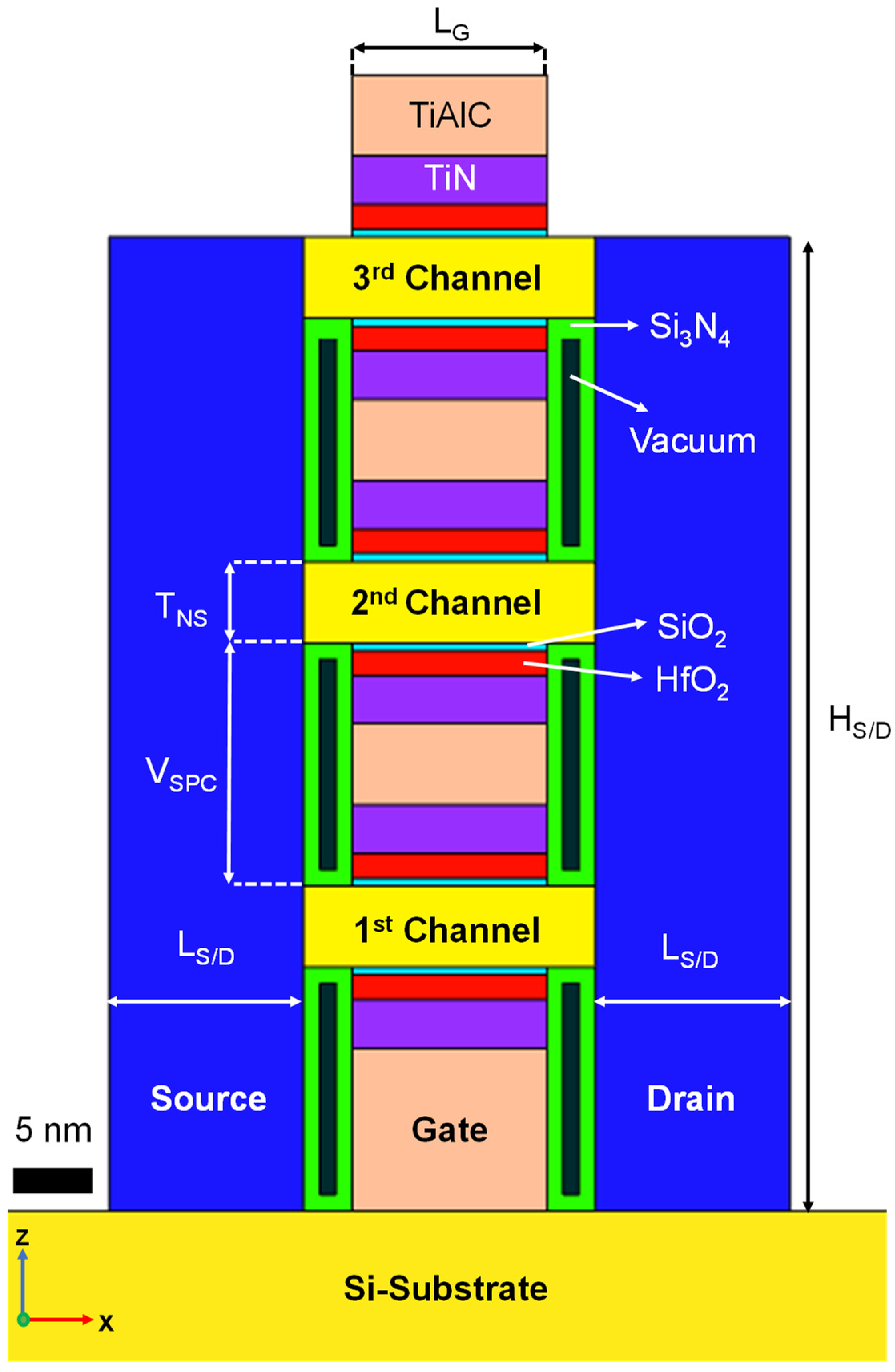
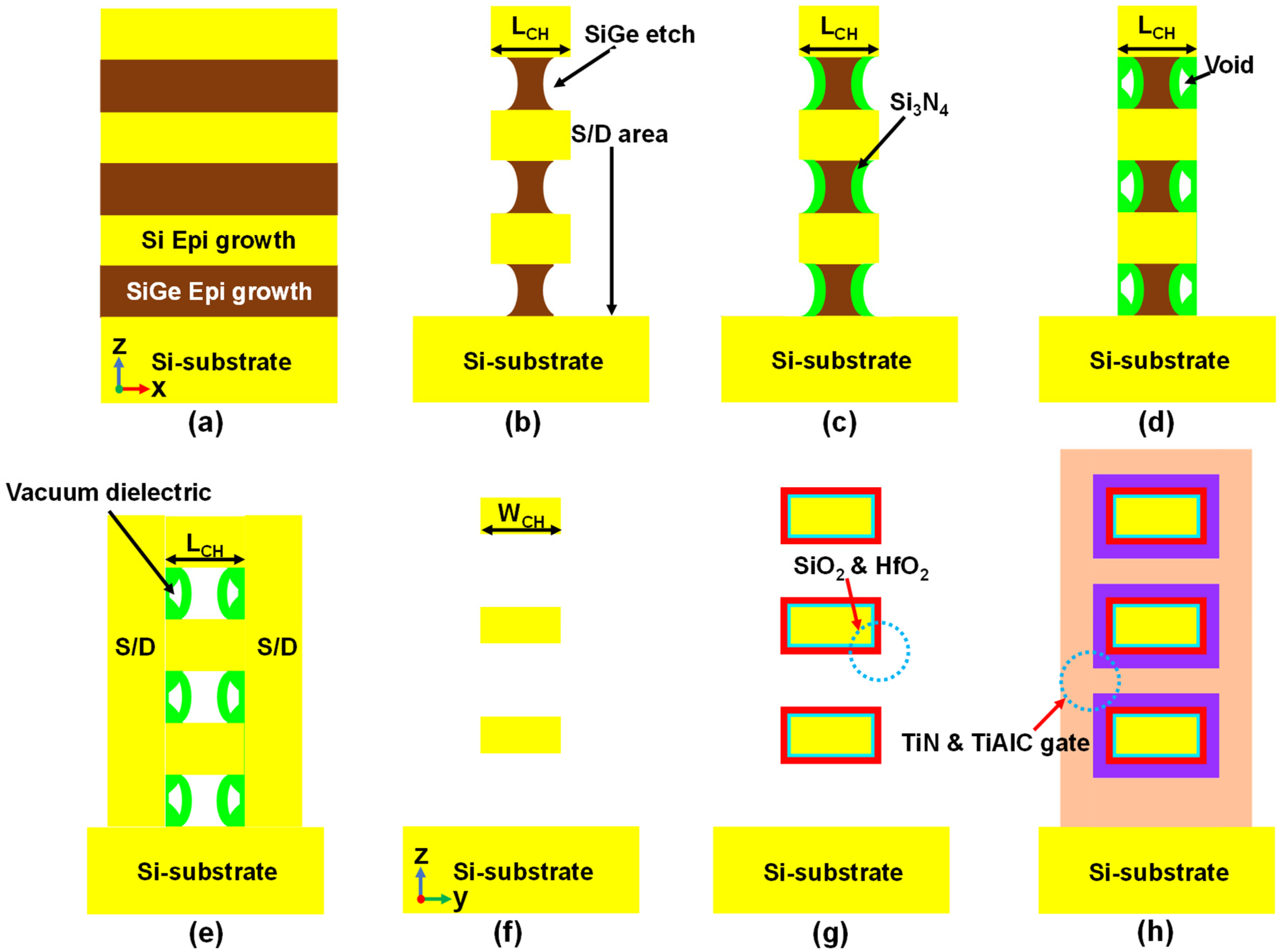
2. Device Structure and Simulation Methodology
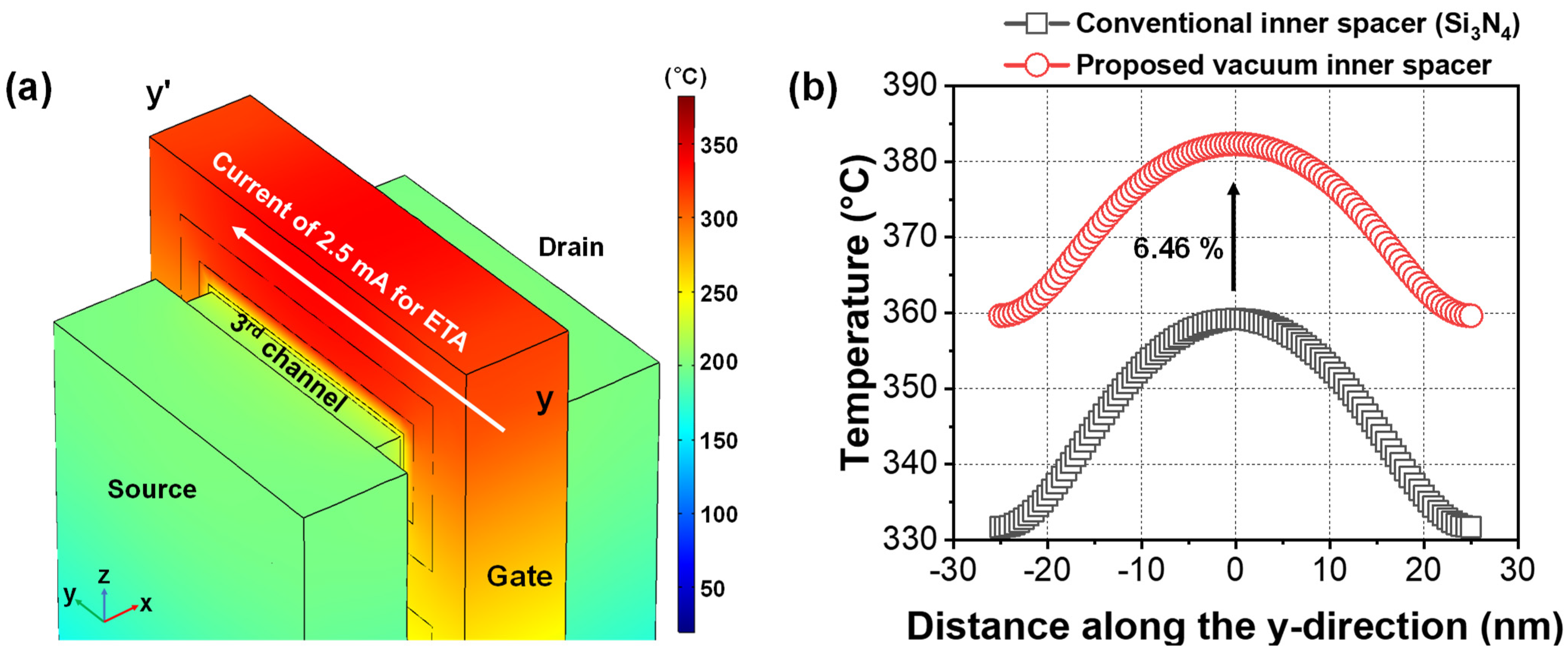
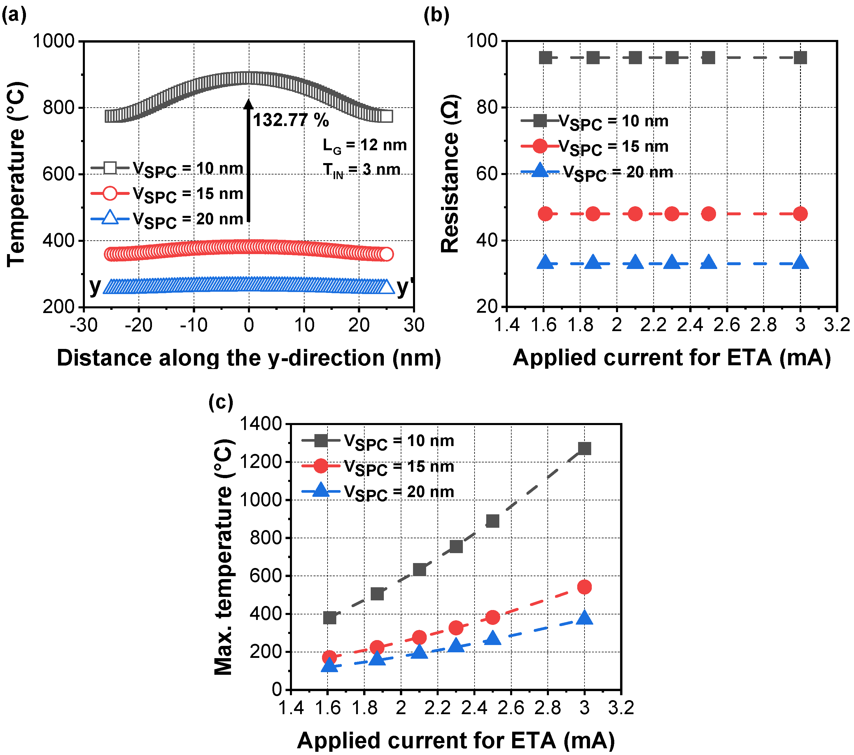
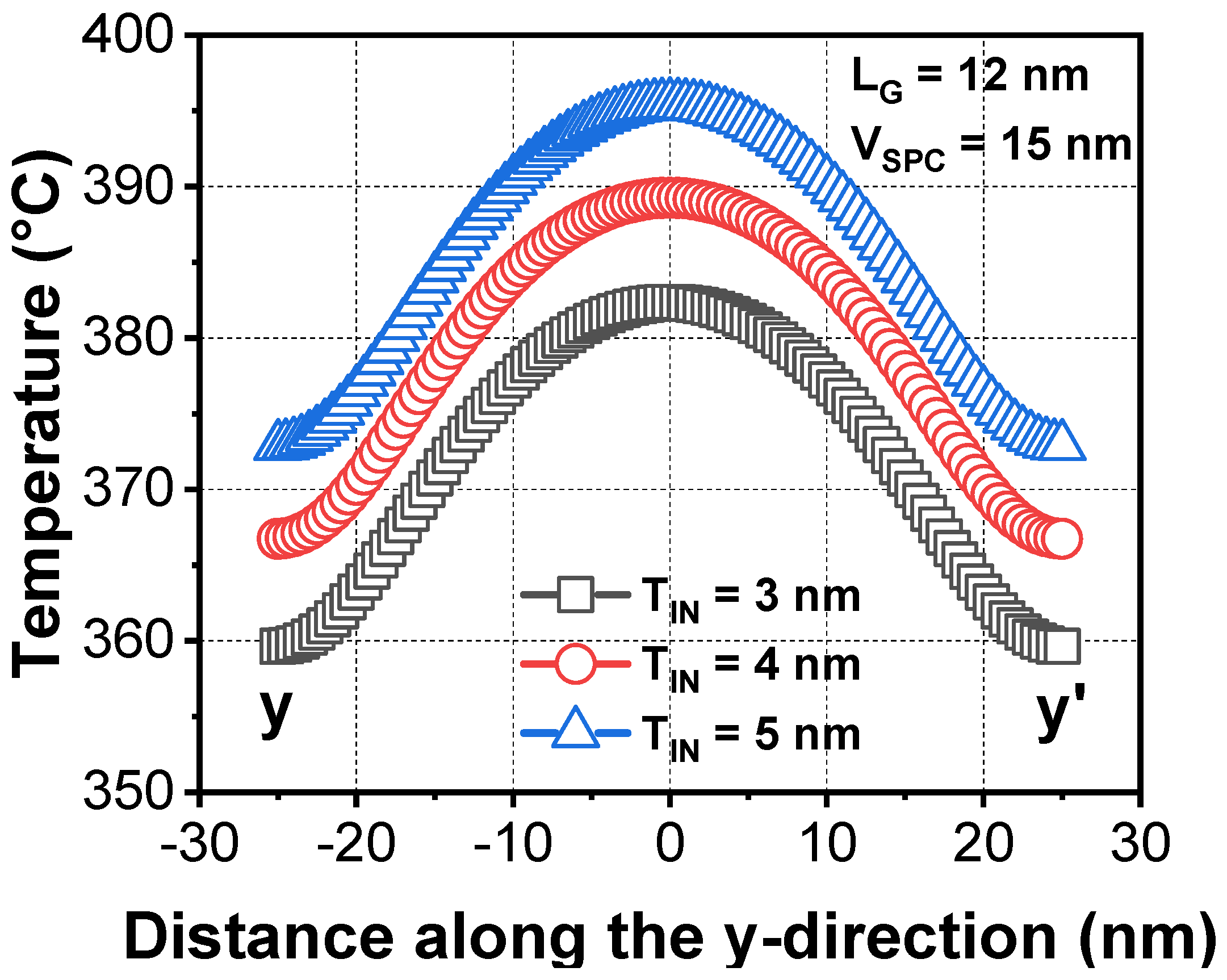
In this study, 3D simulations of the NS FETs with a vacuum inner spacer were performed using COMSOL Multiphysics software. The reason for using COMSOL is because it is the most useful tool for analyzing heat during ETA in nanoscale devices [8,12]. Heat transfer in both the solids module and the electric currents module was used. The simulated environmental conditions were assumed to be air, and the heat transfer coefficient (h) for convective cooling was assumed to be 10 W/m2K. The mesh sizes were varied from 1 nm to 10 nm according to the structure. All simulations were performed under steady-state conditions.
Figure 1 shows a schematic of an NS FET including the vacuum inner spacer. The NS FET has three suspended channels composed of silicon which are surrounded by a high-k and metal gate.
The gate length (LG), channel width (WNS), nanosheet thickness (TNS), and nanosheet-to-nanosheet vertical space (VSPC) were 12 nm, 30 nm, 5 nm, and 15 nm, respectively [13]. The SiO2 and HfO2 interlayers of 1 nm and 3 nm, respectively, were deposited on suspended nanosheets as the gate dielectric. The equivalent oxide thickness (EOT) of the gate dielectric was assumed to be 1.53 nm. In terms of gate module, TiAlC was deposited on TiN as the gate metal [14]. Using vacuum spacer structures has several advantages for logic transistors [15,16,17,18,19]. In particular, in an NS FET, the vacuum inner spacer shows superior AC performance for the device with a low-k inner spacer. The vacuum inner spacer for this work was surrounded by a 1 nm Si3N4 outer shell. Detailed information about the device structure and materials is summarized in Table 1 and Table 2. Then, a current of 2.5 mA was applied through the gate-to-gate method to trigger ETA for Joule heat generation higher temperature than 600 °C [8].

3. Results

Figure 2a shows the heat distribution profile during ETA using gate-to-gate current in an NS FET. During the ETA, the gate temperature was increased beyond 300 °C by Joule heating. The temperature was highest on the surface of the gate electrode, but lowest near the Si substrate, since the Si substrate acted as a heat sink. It was observed that the temperature of the gate surface rose higher than 300 °C, while the temperature in the source and the drain regions remained relatively low because of heat dissipation through the source and drain, which had high thermal conductivity.
Figure 2b shows the extracted temperature of an NS FET with respect to the inner spacer materials. The temperature was extracted after reaching a steady state. During the ETA using gate-to-gate current, most of the Joule heat was concentrated in the middle of the gate electrode, as expected. While curing of the gate dielectric characteristics, on the basis of measured ID–VG or gate leakage (IG), is not included in this work, these electrical results have already been reported several times [8].
When the vacuum inner spacer was included, the temperature during the ETA became 6.46% higher than the case with a conventional inner spacer composed solely of Si3N4. Since the thermal conductivity of the inserted vacuum was 0.024 W/(mK), the low thermally conductive vacuum provided thermal isolation during the ETA. As a result, the annealing effect induced by the ETA could be further improved but with identical power consumption. To improve the annealing effect further, it is desirable to provide guidelines related to device scaling such as LG, TIN, and VSPC. In particular, LG is one of the aggressive design parameters in the minimization of semiconductor devices.
Figure 3a shows the simulated gate surface temperatures considering LG scaling from 16 nm to 8 nm. As the LG decreased from 12 nm to 8 nm, the temperature dramatically increased over 700 °C under an identical power consumption of 2.5 mA. Temperature sensitivity was approximately 80 °C/nm of LG. As LG decreased, the temperature increased due to the increased gate-to-gate resistance, as shown in Figure 3b. As the cross-sectional area of the gate electrode was reduced by LG scaling, the gate-to-gate resistance increased. Hence, the increased voltage drop across the gate-to-gate interval raised the Joule heat temperature [25]. In addition, when current for the ETA was increased from 2.5 mA to 3 mA, the annealing temperature also increased. However, for a relatively long channel device (i.e., LG = 16 nm), it was difficult to generate a sufficiently high temperature to enable gate dielectric curing, even under a current of 3 mA.
Figure 4a shows the simulated surface temperature when VSPC was reduced from 20 nm to 10 nm. The temperature during the ETA increased as the VSPC decreased. The temperature sensitivity with respect to VSPC was approximately 101 °C/nm. Considering the extracted sensitivities, the impact of VSPC was greater than the case with LG scaling. When the VSPC decreased, metal gate height also decreased; hence, the gate-to-gate resistance became larger, as shown in Figure 4b. The increased gate-to-gate resistance gave rise to higher generated Joule heat temperature, as described above. Typically, the Joule heat temperature depends on the applied current density, as shown in Figure 4c. However, when VSPC was longer than 20 nm, insufficient Joule heat was generated to be used for the ETA because of the lowered gate-to-gate resistance. Hence, a VSPC narrower than 15 nm would be preferred for a better annealing effect of NS FETs. This tendency coincides with the development trend of current NS FETs toward a narrower VSPC for better packing density [26].
Figure 5 shows the simulated surface temperature according to vacuum inner spacer thickness (TIN). Modification of the TIN was independent of the gate-to-gate resistance (not shown). However, the temperature sensitivity during the ETA decreased by approximately 6 °C/nm, as the TIN became thinner. This was the effect of increased heat dissipation. As the TIN decreased, thermal resistance in the source/drain (S/D) extension decreased because of reduced extension length. Hence, heat loss through the S/D extension increased [27].
Figure 6 shows the proposed fabrication process flow for an NS FET with a vacuum inner spacer. Multiple Si/SixGe1−x layers are deposited on the Si substrate using iterative epitaxial growth. After dry etching to form the S/D region, the SixGe1−x is selectively indented etched, as shown in Figure 6b. Then, Si3N4 for the shell of the vacuum dielectric is deposited using a poor step coverage process such as plasma-enhanced chemical vapor deposition (PECVD), as shown in Figure 6c,d. The void acts as a vacuum dielectric. Thereafter, nanosheets are released and suspended during the replacement of the poly-Si gate (RPG) process in Figure 6e. Finally, gate stacks including the gate dielectric and work function adjustment metals are deposited.

4. Conclusions

The heat distribution characteristics during the ETA of an NS FET were demonstrated using 3D simulations. When the inner spacer in an NS FET was replaced by a vacuum inner spacer instead of the conventional Si3N4 inner spacer, the temperature generated during the ETA increased by 6.46% under identical power consumption. Device scaling with respect to LG, VSPC, and TIN was investigated in relation to the ETA temperature. The VSPC scaling showed a significant temperature increase with a sensitivity of 101 °C/nm. Moreover, LG scaling showed a temperature increase of 80 °C/nm. However, TIN scaling resulted in a decrease in ETA temperature, and the sensitivity was negligible. As a result, it can be concluded that the proposed NS FET with a vacuum inner spacer is a promising candidate to improve annealing during ETA.

Author Contributions

J.-Y.P. conceptualized this project and designed all the experiments; D.-H.W. conducted all the simulations and wrote this paper; K.-S.L. analyzed the measured data. All authors have read and agreed to the published version of the manuscript.

Funding

This work was supported by the National Research Foundation of Korea (No. 2020M3H2A1076786 and 2021R1F1A1049456). The EDA tool was supported by the IDEC.

Conflicts of Interest

The authors declare no conflict of interest.

References

  1. Chaudhry, A.; Kumar, M.J. Controlling Short-Channel Effects in Deep-Submicron SOI MOSFETs for Improved Reliability: A Review. IEEE Trans. Device Mater. Reliab. 2004, 4, 99–109. [Google Scholar] [CrossRef] [Green Version]
  2. Shen, T.; Watanabe, K.; Zhou, H.; Belyansky, M.; Stuckert, E.; Zhang, J.; Greene, A.; Basker, V.; Wang, M. A new technique for evaluating stacked nanosheet inner spacer TDDB reliability. In Proceedings of the 2020 IEEE International Reliability Physics Symposium (IRPS), Dallas, TX, USA, 28 April–30 May 2020. [Google Scholar] [CrossRef]
  3. Sachid, A.B.; Chen, M.-C.; Hu, C. Bulk FinFET With Low-κ Spacers for Continued Scaling. IEEE Trans. Electron Devices 2017, 64, 1861–1864. [Google Scholar] [CrossRef]
  4. Singh, N.; Agarwal, A.; Bera, L.K.; Liow, T.Y.; Yang, R.; Tung, S.C.; Kumar, R.; Lo, G.Q.; Balasubramanian, N.; Kwong, D.-L. High-Performance Fully Depleted Silicon Nanowire (Diameter ≤ 5 nm) Gate-All-Around CMOS Devices. IEEE Electron Device Lett. 2006, 27, 383–386. [Google Scholar] [CrossRef]
  5. Auth, C.; Cappellani, A.; Chun, J.-S.; Dalis, A.; Davis, A.; Ghani, T.; Glass, G.; Glassman, T.; Harper, M.; Hattendorf, M.; et al. 45 nm High-k + Metal Gate Strain-Enhanced Transistors. In Proceedings of the 2008 Symposium on VLSI Technology, Honolulu, HI, USA, 17–19 June 2008. [Google Scholar] [CrossRef]
  6. Ogura, S.; Tsang, P.J.; Walker, W.W.; Critchlow, D.L.; Shepard, J.F. Design and Characteristics of the Lightly Doped Drain-Source (LDD) Insulated Gate Field-Effect Transistor. IEEE J. Solid-State Circuits 1980, 15, 424–432. [Google Scholar] [CrossRef]
  7. Onishi, K.; Kang, C.S.; Choi, R.; Cho, H.-J.; Gopalan, S.; Nieh, R.E.; Krishnan, S.A.; Lee, J.C. Improvement of Surface Carrier Mobility of HfO2 MOSFETs by High-Temperature Forming Gas Annealing. IEEE Trans. Electron Devices 2003, 50, 384–390. [Google Scholar] [CrossRef]
  8. Park, J.-Y.; Moon, D.-I.; Lee, G.-B.; Choi, Y.-K. Curing of Aged Gate Dielectric by the Self-Heating Effect in MOSFETs. IEEE Trans. Electron Devices 2020, 67, 777–788. [Google Scholar] [CrossRef]
  9. Han, J.-K.; Park, J.-Y.; Kim, C.-K.; Kwon, J.H.; Kim, M.-S.; Hwang, B.-W.; Kim, D.-J.; Choi, K.C.; Choi, Y.-K. Electrothermal Annealing to Enhance the Electrical Performance of an Exfoliated MoS2 Field-Effect Transistor. IEEE Electron Device Lett. 2016, 39, 1532–1535. [Google Scholar] [CrossRef]
  10. Bae, H.; Lee, K.-S.; Ye, P.D.; Park, J.-Y. Current annealing to improve drain output performance of β-Ga2O3 field-effect transistor. Solid-State Electron. 2021, 185, 108134. [Google Scholar] [CrossRef]
  11. Cha, D.-W.; Park, J.-Y. Impact of Dielectrics in SOI FinFET for Lower Power Consumption in Punch-through Current-based Local Thermal Annealing. J. Semicond. Technol. Sci. 2021, 21, 222–228. [Google Scholar] [CrossRef]
  12. Kim, M.-K.; Choi, Y.-K.; Park, J.-Y. Power Reduction in Punch-Through Current-Based Electro-Thermal Annealing in Gate-All-Around FETs. Micromachines 2022, 13, 124. [Google Scholar] [CrossRef]
  13. Lee, K.-S.; Park, J.-Y. Inner Spacer Engineering to Improve Mechanical Stability in Channel-Release Process of Nanosheet FETs. Electronics 2021, 10, 1395. [Google Scholar] [CrossRef]
  14. Xiang, J.; Li, T.; Wang, X.; Han, K.; Li, J.; Zhao, C. Understanding the Role of TiN Barrier Layer on Electrical Performance of MOS Device with ALD-TiN/ALD-TiAlC Metal Gate Stacks TiN 0nm TiN 1nm TiN 2nm TiN 3nm. ESC J. Solid State Sci. Technol. 2016, 5, 327–329. [Google Scholar] [CrossRef]
  15. Chiang, C.K.; Pai, H.; Lin, J.L.; Chang, J.K.; Lee, M.Y.; Hsieh, E.R.; Li, K.S.; Luo, G.L.; Cheng, O.; Chung, S.S. FinFET Plus: A Scalable FinFET Architecture with 3D Air-Gap and Air-Spacer Toward the 3nm Generation and Beyond. In Proceedings of the 2021 International Symposium on VLSI Technology, Systems and Applications (VLSI-TSA), Hsinchu, Taiwan, 19–22 April 2021. [Google Scholar] [CrossRef]
  16. Ko, H.; Kim, J.; Kang, M.; Shin, H. Investigation and Analysis of Dual-k Spacer with Different Materials and Spacer Lengths for Nanowire-FET Performance. Solid-State Electron. 2017, 136, 68–74. [Google Scholar] [CrossRef]
  17. Kim, S.; Cho, W.; Kim, J.; Lee, B.; Park, S. Air-Gap Application and Simulation Results for Low Capacitance in 60nm NAND Flash Memory. In Proceedings of the 22nd IEEE Non-Volatile Semiconductor Memory Workshop, Monterey, CA, USA, 26–30 August 2007. [Google Scholar] [CrossRef]
  18. Sachid, A.B.; Huang, Y.-M.; Chen, Y.-J.; Chen, C.-C.; Lu, D.D.; Chen, M.-C.; Hu, C. FinFET With Encased Air-Gap Spacers for High-Performance and Low-Energy Circuits. IEEE Electron Device Lett. 2016, 38, 16–19. [Google Scholar] [CrossRef]
  19. Pundir, Y.P.; Bisht, A.; Saha, R.; Pal, P.K. Air-spacers as analog-performance booster for 5nm-node N-channel nanosheet transistor. Semicond. Sci. Technol. 2021, 36, 10. [Google Scholar] [CrossRef]
  20. Loubet, N.; Hook, T.; Montanini, P.; Yeung, C.-W.; Kanakasabapathy, S.; Guillom, M.; Yamashita, T.; Zhang, J.; Miao, X.; Wang, J.; et al. Stacked nanosheet gate-all-around transistor to enable scaling beyond FinFET. In Proceedings of the IEEE 2017 Symposium on VLSI Technology, Kyoto, Japan, 5–8 June 2017. [Google Scholar] [CrossRef]
  21. Abe, S.; Miyazawa, Y.; Nakajima, Y.; Hanajiri, T.; Toyabe, T.; Sugano, T. Suppression of DIBL in deca-nano SOI MOSFETs by controlling permittivity and thickness of BOX layers. In Proceedings of the 2009 10th International Conference on Ultimate Integration of Silicon, Aachen, Germany, 18–20 March 2009. [Google Scholar] [CrossRef]
  22. Cai, L.; Chen, W.; Du, G.; Zhang, X.; Liu, X. Layout Design Correlated with Self-Heating Effect in Stacked Nanosheet Transistors. IEEE Trans. Electron Devices 2018, 65, 2647–2653. [Google Scholar] [CrossRef]
  23. Sachid, A.B.; Lin, H.-Y.; Hu, C. Nanowire FET With Corner Spacer for High-Performance, Energy-Efficient Applications. IEEE Trans. Electron Devices 2017, 64, 5181–5187. [Google Scholar] [CrossRef]
  24. Zhang, Y.; Zhang, Y.; Bakir, M.S. Thermal Design and Constraints for Heterogeneous Integrated Chip Stacks and Isolation Technology Using Air Gap and Thermal Bridge. IEEE Trans. Compon. Packag. Manuf. Technol. 2014, 4, 1914–1924. [Google Scholar] [CrossRef]
  25. Park, J.-Y.; Moon, D.-I.; Seol, M.-L.; Kim, C.-K.; Jeon, C.-H.; Bae, H.; Bang, T.; Choi, Y.-K. Self-Curable Gate-All-Around MOSFETs Using Electrical Annealing to Repair Degradation Induced from Hot-Carrier Injection. IEEE Trans. Electron Devices 2016, 63, 910–915. [Google Scholar] [CrossRef]
  26. Lee, K.-S.; Park, J.-Y. N-Type Nanosheet FETs without Ground Plane Region for Process Simplification. Micromachines 2022, 13, 432. [Google Scholar] [CrossRef]
  27. Ota, K.; Saitoh, M.; Tanaka, C.; Numata, T. Experimental Study of Self-Heating Effects in Trigate Nanowire MOSFETs Considering Device Geometry. IEEE Trans. Electron Devices 2012, 59, 3239–3242. [Google Scholar] [CrossRef]
Figure 1. Cross-sectional schematic of an NS FET with vacuum inner spacer for ETA simulations.
Micromachines 13 00987 g001
Figure 2. (a) Simulated heat distribution profile during ETA using gate-to-gate current in an NS FET. (b) Extracted temperature on the gate surface according to inner spacer material.
Micromachines 13 00987 g002
Figure 3. (a) Extracted temperature during the ETA in an NS FET with vacuum dielectric with respect to LG. Extracted (b) gate to-gate resistance and (c) maximum temperature with various applied currents for the ETA, respectively. Inner spacer thickness (TIN) was fixed to 3 nm regardless of LG.
Micromachines 13 00987 g003
Figure 4. (a) Extracted temperature during the ETA in an NS FET with vacuum dielectric with various VSPC. Extracted (b) gate-to-gate resistance and (c) surface temperature with respect to VSPC and applied current, respectively.
Micromachines 13 00987 g004
Figure 5. Extracted temperature during the ETA with various inner spacer thickness (TIN).
Micromachines 13 00987 g005
Figure 6. Proposed fabrication process flow of an NS FET with vacuum inner spacer. (a) Si/SixGe1−x epitaxial growths on Si substrate. (b) SixGe1−x indent etching. (c,d) Inner spacer deposition with void formation. (e,f) S/D epitaxial growth and suspended multiple nanosheet formation. (g,h) Gate dielectric and metal gate deposition.
Micromachines 13 00987 g006
Table 1. Device geometric information for simulations.
ParametersMaterialsValues
Gate length, LGTiAlC12 nm [20]
Channel width, WNSSi30 nm [13]
Nanosheet thickness, TNSSi5 nm [13]
Inner spacer thickness, TINSi3N43 nm [13]
Nanosheet-to-nanosheet vertical space, VSPC-15 nm
Gate dielectric SiO2/HfO21/3 nm
Source/drain length, LS/DSi12 nm [13]
Source/drain height, HS/DSi60 nm
Vacuum dielectricVacuum1 nm
Table 2. Material properties for simulations.
MaterialRelative
Permittivity
Thermal
Conductivity
(W/mK)
Electrical Conductivity
(S/m)
Si11.90 [21]Si substrate
140 [22]
7.68 × 10⁻³
Channels
18 [22]
7.68 × 10⁻³
Source/drain
38 [22]
5 × 10⁵
Si3N47.50 [23]3.21 × 10⁻⁸
SiO23.90 [21]1.41 × 10⁻¹⁷
HfO2221.061 × 10−14
TiAlC1462. × 106
Vacuum1 [21,23]0.024 [24]1 × 10⁻¹⁵
Publisher’s Note: MDPI stays neutral with regard to jurisdictional claims in published maps and institutional affiliations.

