Abstract
The application of GaN HEMTs on silicon substrates in high-voltage environments is significantly limited due to their complex buffer layer structure and the difficulty in controlling wafer warpage. In this work, we successfully fabricated GaN power HEMTs on 6-inch sapphire substrates using a CMOS-compatible process. A 1.5 µm thin GaN buffer layer with excellent uniformity and a 20 nm in situ SiN gate dielectric ensured uniformly distributed VTH and RON across the entire 6-inch wafer. The fabricated devices with an LGD of 30 µm and WG of 36 mm exhibited an RON of 18.06 Ω·mm and an off-state breakdown voltage of over 3 kV. The electrical mapping visualizes the high uniformity of RON and VTH distributed across the whole 6-inch wafer, which is of great significance in promoting the applications of GaN power HEMTs for medium-voltage power electronics in the future.
1. Introduction
GaN HEMTs possess excellent material and device characteristics, such as high electron mobility, high critical electric field, and low switching losses. These features have led GaN to significant success in the field of power electronics, with widespread applications in power supplies, data centers, LiDAR systems, and consumer electronics [1,2,3,4,5]. So far, the three semiconductor materials Si, SiC, and GaN have achieved large-scale production and commercialization. Various silicon devices are used across different voltage ranges. SiC has also been commercialized in the medium-voltage range, and devices with voltages as high as 10 kV have been reported. However, owing to GaN’s superior physical properties that enable higher switching frequencies, GaN is destined to revolutionize the field of power electronics [6,7,8,9].
Currently, most commercial GaN HEMTs are based on large-diameter, low-cost Si substrates [3,10]. However, the complex buffer layer structure [11,12] and difficulty in controlling warpage in GaN HEMTs on silicon substrates limit their applications in medium–voltage power electronics. In recent years, substrates such as sapphire, SiC [13,14], SOI [15], and QST [16] have emerged. Among these, sapphire has been actively explored recently due to its low cost and high mechanical strength [17].
Recently, Transphorm reported the development of 1.2 kV GaN switches on sapphire, achieving over 99% efficiency for a 900:450 V hard-switched buck converter [18,19]. Subsequently, e-mode p-GaN gate HEMTs on sapphire substrates with a high breakdown voltage (VBD) of 1.4 kV were demonstrated [20]. Further, we have fabricated 1.7 kV d-mode GaN HEMTs on a 1.5 µm ultra-thin buffer [21] and 8 kV GaN HEMTs using CMOS-compatible processing [22], and reported e-mode p-GaN gate HEMTs on 6-inch sapphire [23], and d-mode GaN HEMTs on 8-inch sapphire [24], which are promising for ≥650 V power applications. Li et al. reported the 1.2 kV GaN half bridges monolithically integrated on sapphire substrates [25]. Lu et al. reported that GaN HEMTs fabricated on sapphire possess an ultrahigh breakdown voltage (VBD) exceeding 1.9 kV [26]. It should be noted that most research is based on small transistors that cannot be applied in real applications. Therefore, ≥3 kV GaN power HEMTs are strongly needed.
In this work, we present the epitaxy and fabrication of ≥3 kV GaN power HEMTs on 6-inch sapphire substrates using a CMOS-compatible process for the first time. Then, wafer-level uniformity is preliminarily assessed. Afterwards, the blocking capability is evaluated through off-state breakdown characterization, and the capacitance–voltage characteristics are probed. Finally, the threshold voltage instability of the devices is characterized.
2. Materials and Methods
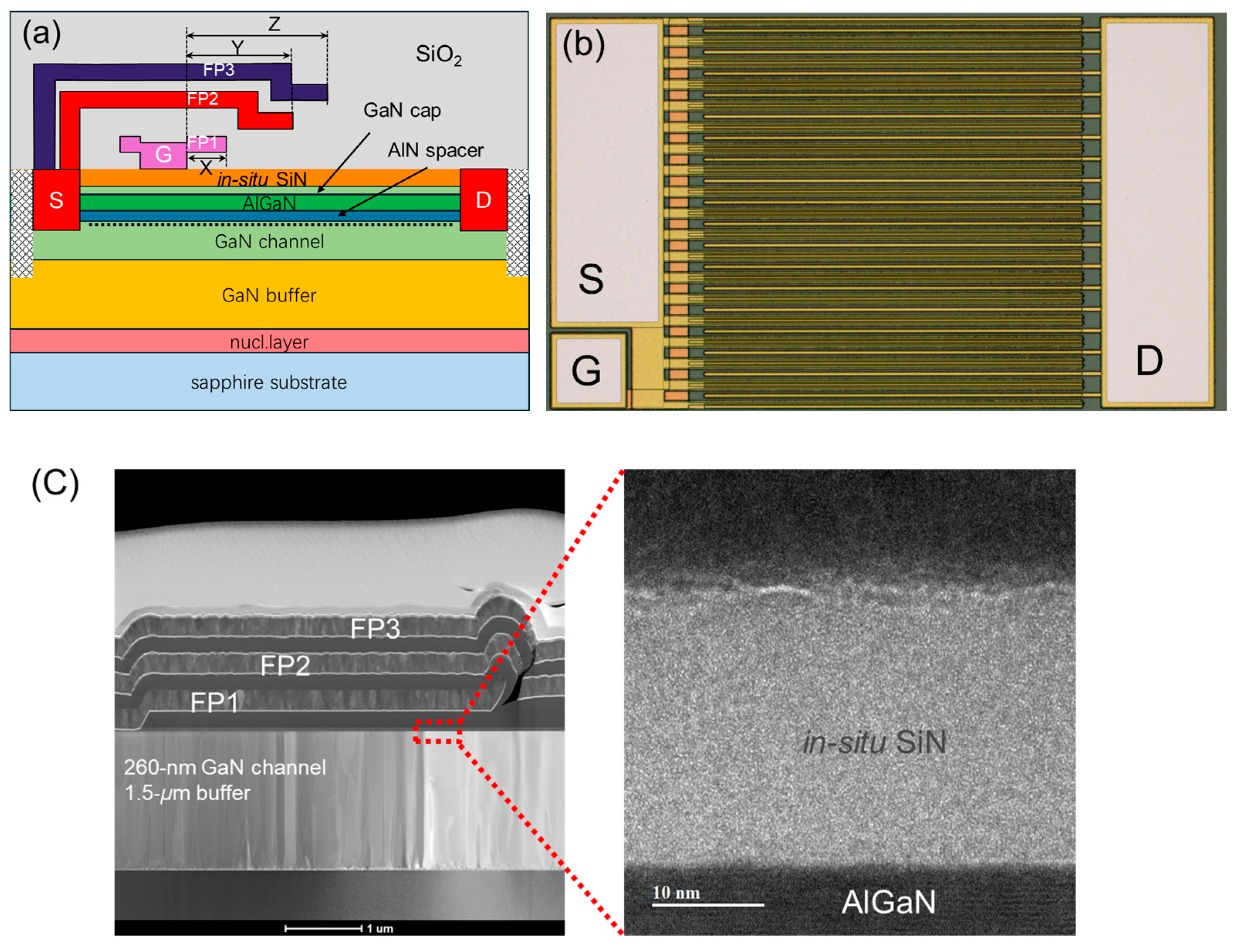
The GaN power HEMT structure was grown on 6-inch sapphire substrates using metal–organic chemical vapor deposition (MOCVD), as shown in Figure 1, which comprises a 35 nm AlGaN nucleation layer, a 1.5 μm GaN buffer layer, a 260 nm GaN channel layer, a 1 nm AlN spacer, a 20 nm Al0.25GaN barrier layer, a 5 nm GaN cap layer, and a 20 nm in situ SiN, as depicted in Figure 2a. The in situ SiN forms the gate dielectric of the transistor and also serves as the passivation layer. Figure 2c shows an SEM and TEM of the 20 nm in situ SiN and the AlGaN–in situ SiN interface.

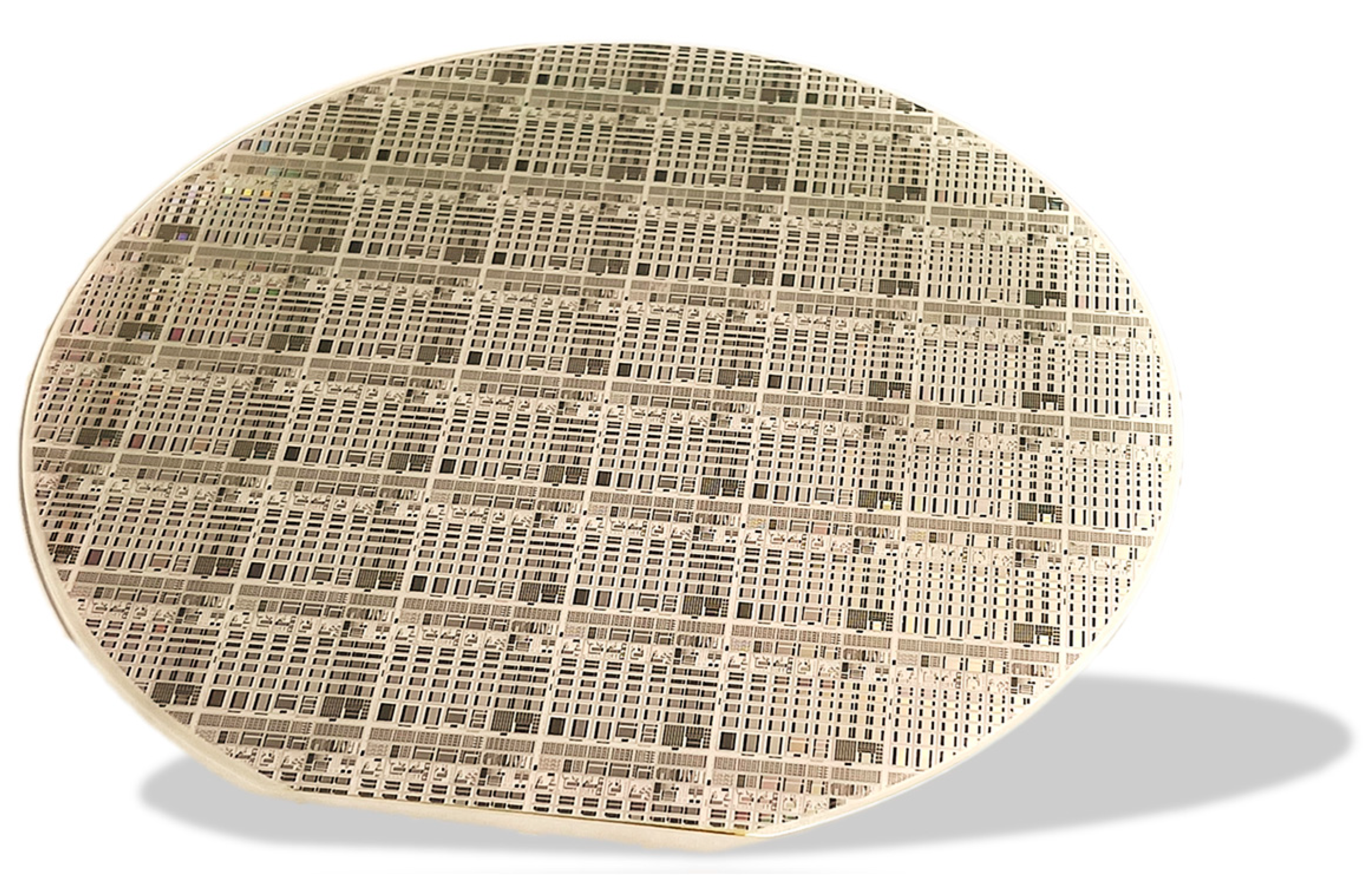
Figure 1.
Photograph of the GaN power HEMTs on a 6-inch sapphire wafer manufactured by a CMOS-compatible process.

Figure 2.
(a) Cross-sectional schematic of the fabricated GaN power HEMTs on 6-inch sapphire, (b) top view of the fabricated 36 mm GaN power HEMTs with in situ SiN as the gate dielectric, and (c) SEM and TEM images of the GaN power HEMTs on sapphire. The thickness of the field plate metal is approximately 300 nm.
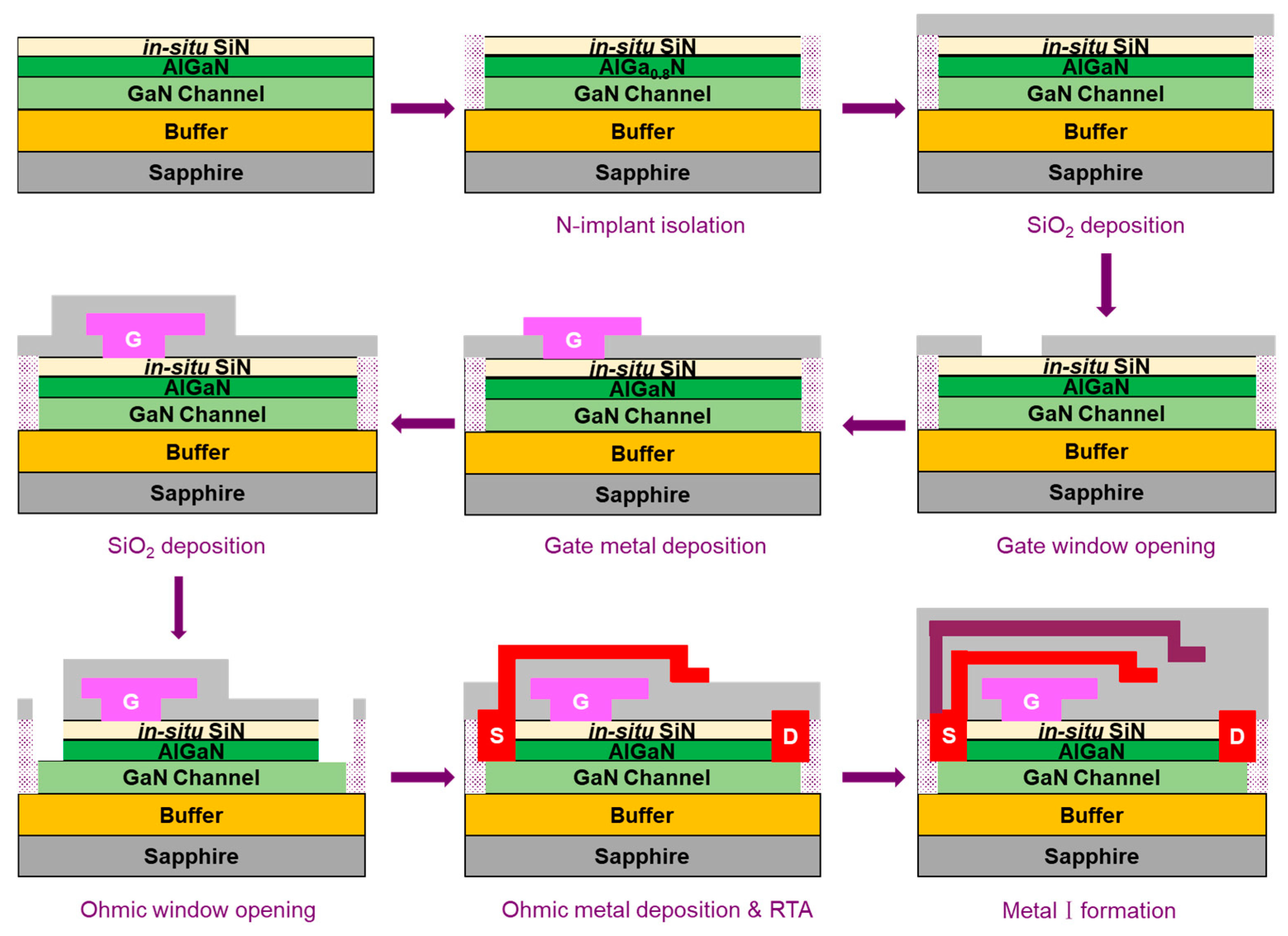
As shown in Figure 3, the device fabrication started with patterning lithography marks. Device isolation was then performed using N implantation. Next, a 150 nm SiO2 layer was deposited by plasma-enhanced chemical vapor deposition (PECVD), and the gate window was opened via reactive ion etching (RIE). Gate metal was deposited via physical vapor deposition (PVD), followed by gate metal patterning using inductively coupled plasma (ICP) etching. The gate metal stack comprises Ti/Al/Ti (20/250/20 nm), under which is the 20 nm in situ SiN dielectric. The gate processing was finalized by the deposition of a second SiO2 layer by PECVD. Next, Ohmic contact window opening was performed by RIE and ICP to remove the dielectric and AlGaN barrier, followed by Ti/Al (10/200 nm) Ohmic metal stack deposition and rapid thermal annealing at 565 °C for 90 s in the ambient of N2. Finally, after the deposition of a third SiO2 layer, Metal I of Ti/Al/Ti (20/250/20 nm) metal stack was deposited by PECVD and then patterned by ICP etching.
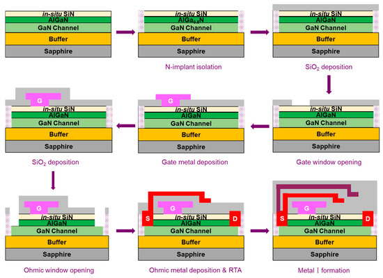
Figure 3.
Processing flow of the GaN power HEMTs on 6-inch sapphire.
The fabricated power HEMTs have a gate width (WG) of 36 mm, a gate length (LG) of 4 μm, a gate–source distance (LGS) of 1.5 μm, and various gate–drain distances (LGD) ranging from 6 μm to 30 μm, as depicted in Figure 2b. The device includes three field plates, denoted as [X, Y, Z], which are formed by gate metal, Ohmic metal, and Metal I, as shown in Figure 2c. The electrical characterizations were performed using Keysight B1500A and B1505A (Keysight Technologies, one of the company’s global core sites, is located in Santa Rosa, CA, USA).
3. Results
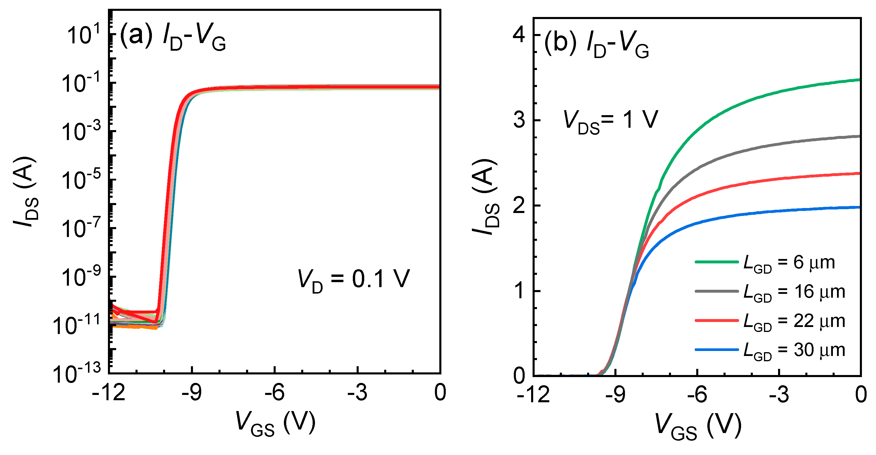
Figure 4a displays the typical transfer characteristics of the GaN power HEMTs with an LGD of 6/16/22/30 μm, on which we can see the VTH is concentrated around −9.5 V under the criterion of IDS = 0.1 mA/mm, attributed to the uniformly deposited in situ SiN under the gate. It can also be observed that the curves exhibit almost no hysteresis. The SS value is 104 mV/decade, and the mobility is 1561 cm2/V·s.
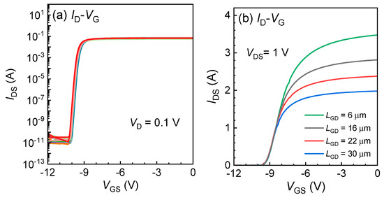
Figure 4.
(a) The logarithmic and (b) linear transfer characteristics of the GaN power HEMTs with an LGD of 6/16/22/30 μm on 6-inch sapphire.
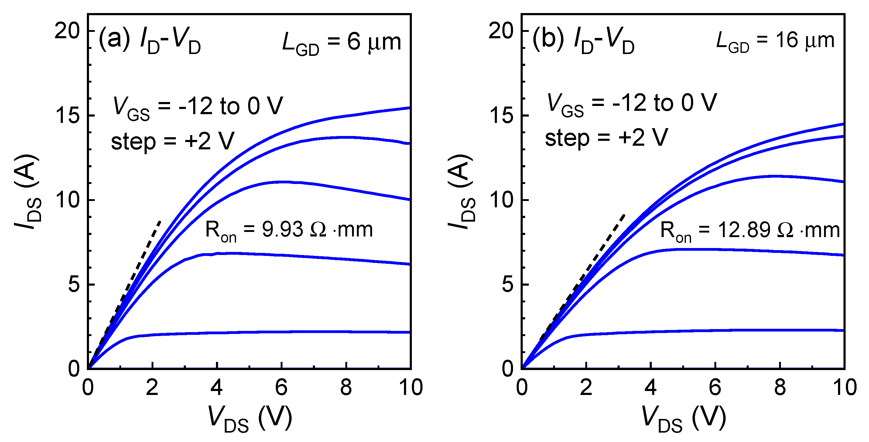
Figure 5 displays the typical output characteristics of the fabricated GaN power HEMTs with various LGD ranging from 6 to 30 μm. At VGS = 0 V, the on-state saturation current is 15.4 A with an LGD of 6 μm, as shown in Figure 5a. Figure 5b,c respectively show the on-state saturation current and RON for LGD of 16 µm and 22 µm. The device exhibits an on-state saturation drain current of 355 mA/mm and an on-state resistance of 18.06 Ω·mm with an LGD of 30 μm, as shown in Figure 5d.
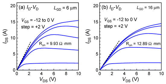
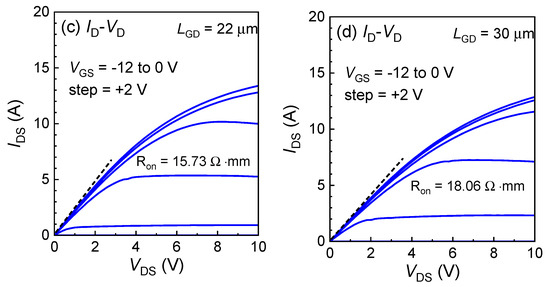
Figure 5.
Output characteristics of the GaN power HEMTs with an LGD of 6/16/22/30 μm on 6-inch sapphire.
The electrical mapping of VTH and RON was summarized to verify the uniformity of the 6-inch wafer. As shown in Figure 6, the VTH values are concentrated in the range of −10 to −9 V, and the RON values are concentrated in the range of 18 to 19 Ω·mm for the GaN power HEMTs with an LGD of 30 μm. The relatively high uniformity can be attributed to the uniform in situ SiN and the precise etch-stop technique used during gate window opening.
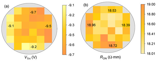
Figure 6.
Electrical mapping of (a) VTH and (b) RON of the fabricated GaN power HEMTs with an LGD of 30 μm across the 6-inch sapphire wafer.
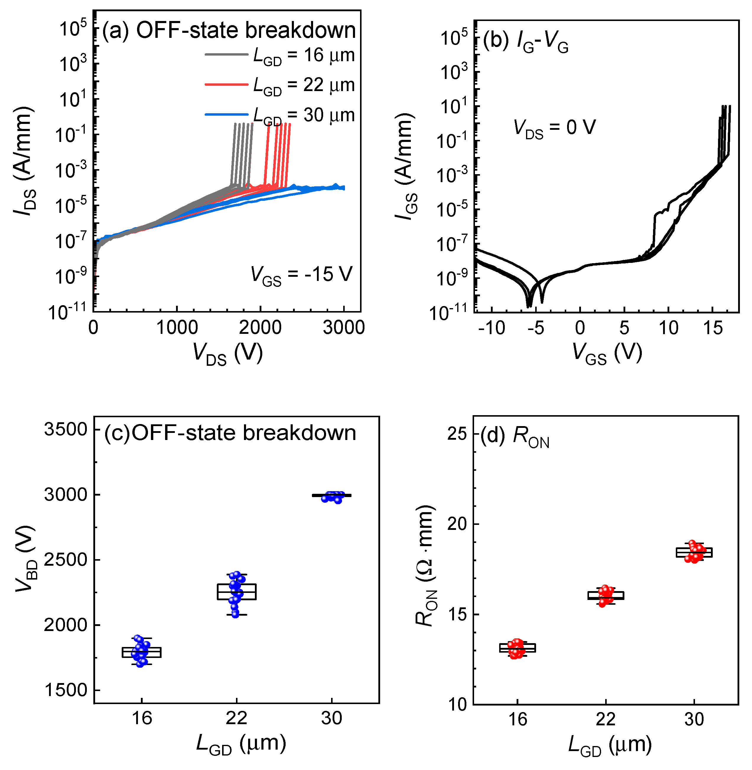
Next, the OFF-state breakdown characteristics of the fabricated GaN power HEMTs with various LGD ranging from 16 to 30 μm were probed. As shown in Figure 7a, generally, GaN power HEMTs exhibit excellent blocking capability, with VBD reaching 3 kV for an LGD of 30 μm. The boxplots of OFF-state breakdown and RON are presented in Figure 7c,d, respectively. Devices with different LGD values exhibit high breakdown voltages and excellent uniformity, which highlights the potential of the GaN power HEMTs on sapphire for future medium- to high-voltage applications. As shown in Figure 7b, the gate forward breakdown voltage (VGS) reaches 16 V, owing to the high-quality and highly uniform in situ SiN. The successful fabrication of ≥3 kV GaN power HEMTs is of great significance for driving the revolution in power electronics.
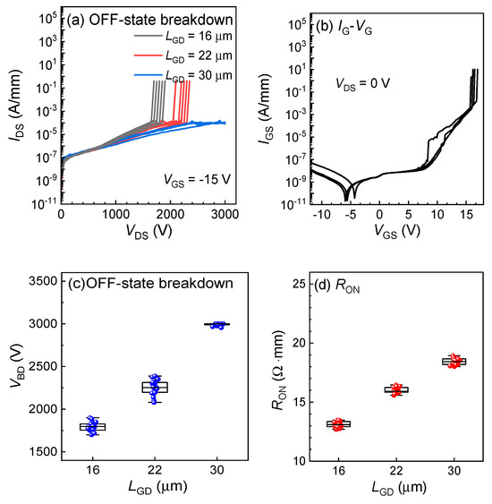
Figure 7.
(a) OFF-state breakdown characteristics with various LGD and (b) forward IG-VG measurement of the GaN power HEMTs on 6-inch sapphire. The statistical distribution of VBD (c) and RON (d) versus LGD.
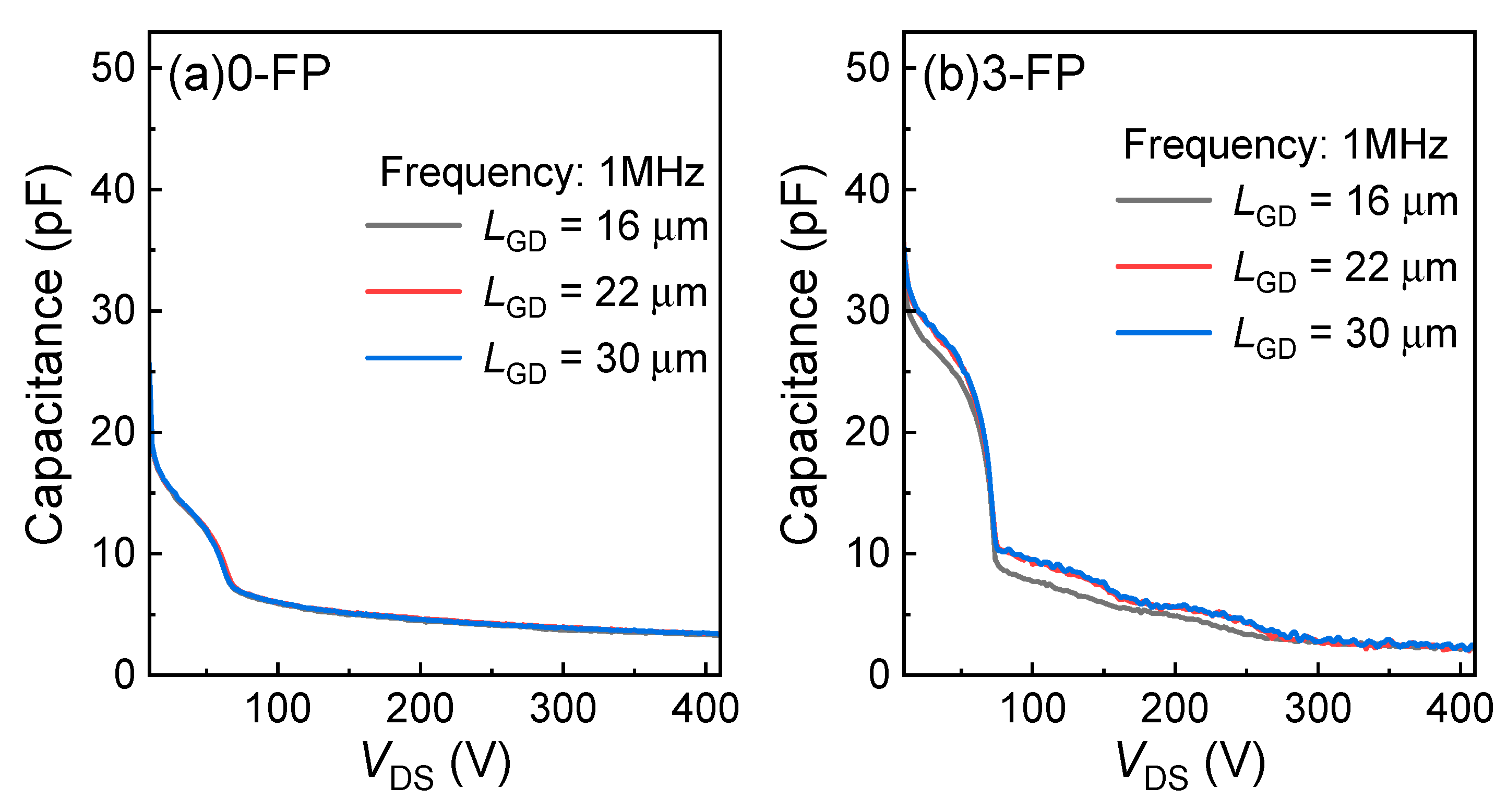
The capacitance–voltage characteristics (CGD) of GaN power HEMTs with different field plate structures in the OFF state were evaluated, as plotted in Figure 8. It can be seen from Figure 8a that the 0-FP HEMTs exhibit lower capacitance values, and the capacitance values remain consistent for different LGD. As shown in Figure 8b, the capacitance values for different LGD exhibit significant differences. Moreover, the capacitances are strongly modulated by the field plate structure. Three field plate structures, [2.25 3.75 6.75], [2.25 4.75 8.75], and [2.25 4.75 8.75], correspond to LGD values of 16, 22, and 30 μm, respectively.
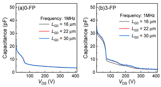
Figure 8.
The CGD characteristics of (a) the 0-FP GaN HEMTs and (b) the 3-FP GaN HEMTs with various structures. The measurement frequency is 1 MHz.
Bias Temperature Instability (BTI) is a crucial reliability issue, as it generates interface traps and oxide charges that degrade the performance of HEMTs, which could trigger malfunctions in the power system during operation.
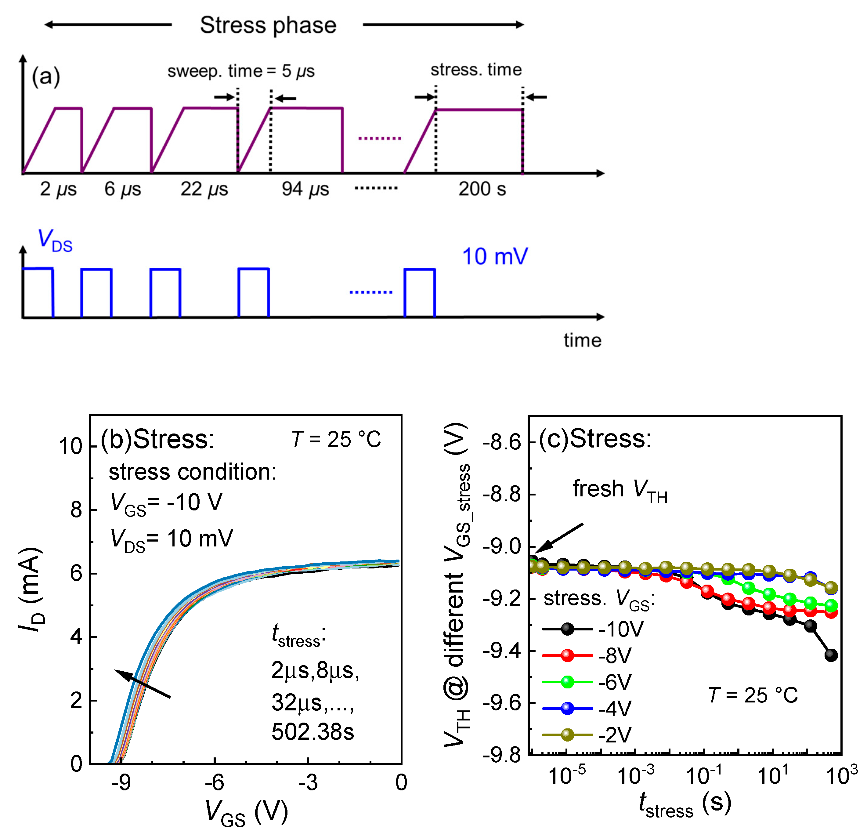
In this work, BTI measurements were performed to examine the VTH stability under gate stress using fast sweeping characterization with a Keysight B1530A WGFMU (Waveform Generator/Fast Measurement Unit). During the measurements, as shown in Figure 9a, the stress was periodically interrupted to measure the ID-VG curves by sweeping the VGS from −10 to 0 V within 5 μs. For negative gate stress, VTH decreases with stressing time and the magnitude of stress voltage, as shown in Figure 9b. Figure 9c summarizes the BTI performance of the GaN power HEMTs under various VGS, and the VTH shift was kept to as low as −0.36057 V corresponding to a VGS of −10 V, thanks to the high-quality in situ SiN.
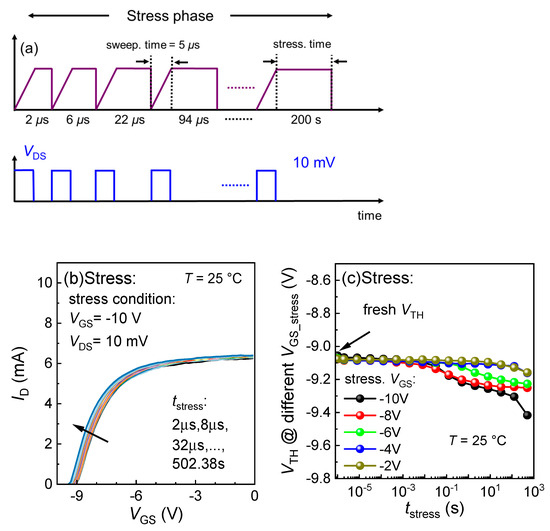
Figure 9.
(a) Sketches of BTI measurement sequences using fast sweeping over 5 μs in this work, (b) ID-VG curves during the stressing phase by stressing VGS of −10 V, and (c) VTH evolution under different stress VGS from −10 to −2 V during the stressing phase at 25 °C. The fast VGS sweeps from −10 to 0 V in 5 μs. VTH is extracted at IDS = 0.1 mA/mm.
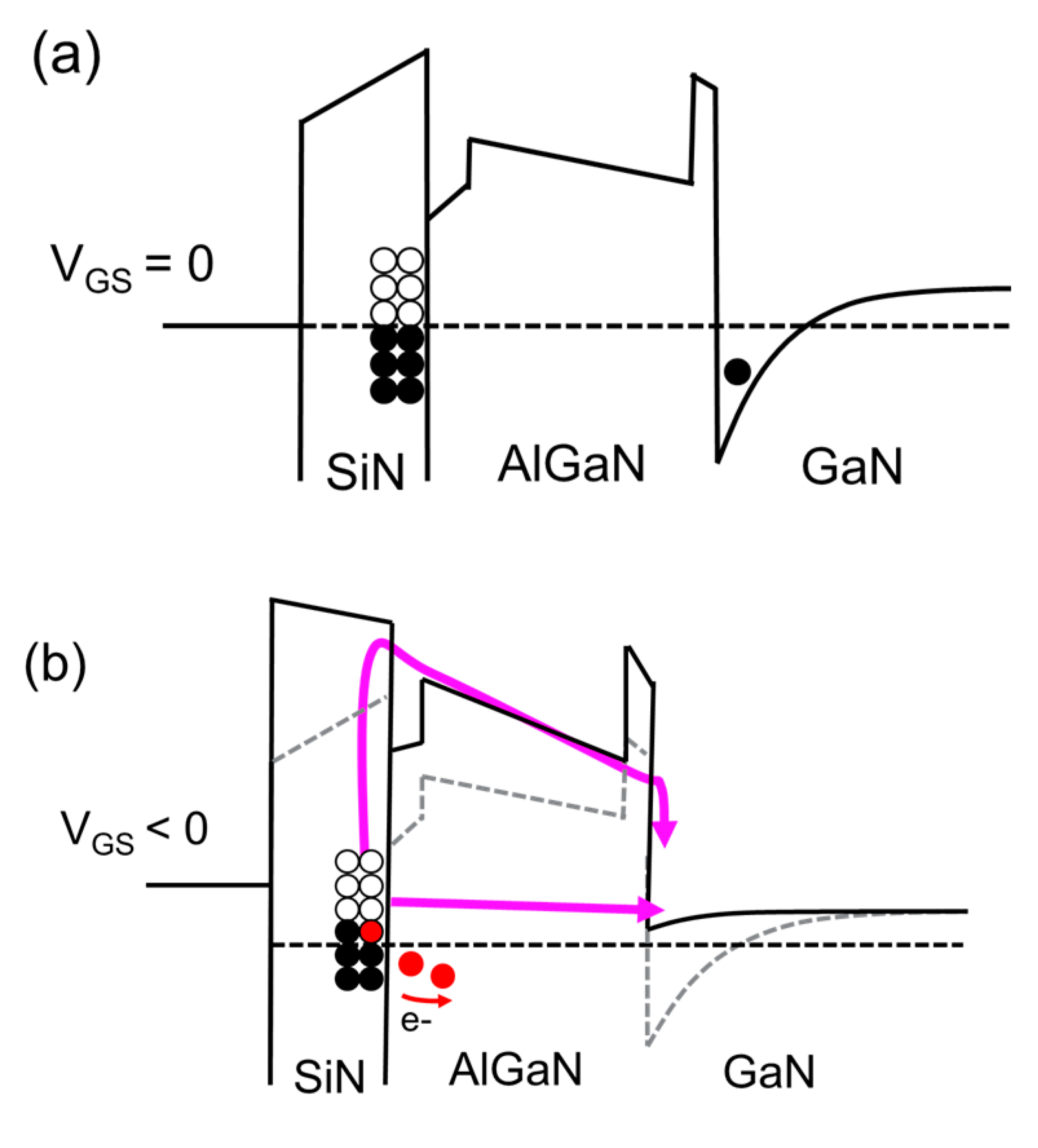
Figure 10 shows the schematic band diagram of the metal/in situ SiN/GaN/AlGaN/AlN/GaN gate stack under negative gate bias stress. The conduction band and the occupation of traps are shown in Figure 10a under thermal equilibrium, where all electrons below the Fermi level are filled. Open and filled circles indicate empty and filled traps, respectively. During BTI stress, part of the border traps in the SiN should be able to discharge, either by tunneling through the AlGaN barrier or via trap-assisted conduction, inducing a negative VTH shift [27].

Figure 10.
Schematic band diagram of the metal/in situ SiN//GaN/AlGaN/AlN/GaN gate stack under (a) VGS = 0 V and (b) negative gate bias stress.
Table 1 shows a comparison of our GaN HEMTs on 6-inch sapphire substrates with other reported works. The devices in this work show excellent performance in terms of ION/IOFF, SS, IDS, RON,SP, RON, VBD, and VBD/LGD. These results indicate their potential for high-power applications.

Table 1.
Comparison of GaN HEMTs.
4. Conclusions
The GaN power HEMTs on 6-inch sapphire with an OFF-state breakdown voltage exceeding 3 kV have been successfully fabricated using a CMOS-compatible process in our pilot line. The 1.5 μm thin buffer and in situ SiN together guarantee high uniformity across the whole wafer. A preliminary evaluation of the device’s gate threshold voltage instability was conducted. The fabricated power HEMTs exhibit a low RON, a low OFF state leakage current, and a high breakdown voltage, verifying the high quality and high uniformity of the 6-inch wafer. The remarkably simple epitaxy process and device structures, combined with the use of large-scale and low-cost sapphire substrates, can facilitate the application of GaN in the medium-voltage market in the future.
Author Contributions
Device design, X.L. and S.Y.; fabrication, J.J., X.L., L.C., L.W. and Z.L.; characterization, J.Z. and X.L.; writing—original draft preparation, J.Z., X.L., Y.H. and J.Z. (Jincheng Zhang). All authors have read and agreed to the published version of the manuscript.
Funding
This research was funded by the National Key Research and Development Program of China, grant number 2021YFB3600900.
Data Availability Statement
The data that support the findings of this study are available from the corresponding authors upon reasonable request.
Acknowledgments
The authors thank the engineering team at the Guangzhou Wide Bandgap Semiconductor Innovation Center, especially Wenjuan Zhang, Qiang Mei, Xincheng Li, Fuda Liao, and Wenzhen Chen.
Conflicts of Interest
Authors Long Chen, Lezhi Wang and Zilan Li were employed by the company Guangdong Ziener Technology Co., Ltd. The remaining authors declare that the research was conducted in the absence of any commercial or financial relationships that could be construed as a potential conflict of interest.
References
- Jones, E.A.; Wang, F.F.; Costinett, D. Review of Commercial GaN Power Devices and GaN-Based Converter Design Challenges. IEEE J. Emerg. Sel. Top. Power Electron. 2016, 4, 707–719. [Google Scholar] [CrossRef]
- Amano, H.; Baines, Y.; Beam, E.; Borga, M.; Bouchet, T.; Chalker, P.R.; Charles, M.; Chen, K.J.; Chowdhury, N.; Chu, R.; et al. The 2018 GaN power electronics roadmap. J. Phys. D Appl. Phys. 2018, 51, 163001. [Google Scholar] [CrossRef]
- Chen, K.J.; Haberlen, O.; Lidow, A.; lin Tsai, C.; Ueda, T.; Uemoto, Y.; Wu, Y. GaN-on-Si power technology: Devices and applications. IEEE Trans. Electron. Devices 2017, 64, 779–795. [Google Scholar] [CrossRef]
- Hoo Teo, K.; Zhang, Y.; Chowdhury, N.; Rakheja, S.; Ma, R.; Xie, Q.; Palacios, T. Emerging GaN technologies for power, RF, digital, and quantum computing applications: Recent advances and prospects. J. Appl. Phys. 2021, 130, 160902. [Google Scholar] [CrossRef]
- Islam, N.; Mohamed, M.F.P.; Khan, M.F.A.J.; Falina, S.; Kawarada, H.; Syamsul, M. Reliability, applications and challenges of GaN HEMT technology for modern power devices: A review. Crystals 2022, 12, 1581. [Google Scholar] [CrossRef]
- Flack, T.J.; Pushpakaran, B.N.; Bayne, S.B. GaN Technology for Power Electronic Applications: A Review. J. Electron. Mater. 2016, 45, 2673–2682. [Google Scholar] [CrossRef]
- Wang, J.; Zhao, T.; Li, J.; Huang, A.Q.; Callanan, R.; Husna, F.; Agarwal, A. Characterization, modeling, and application of 10-kV SiC MOSFET. IEEE Trans. Electron. Devices 2008, 55, 1798–1806. [Google Scholar] [CrossRef]
- Huang, X.; Liu, Z.; Lee, F.C.; Li, Q. Characterization and Enhancement of High-Voltage Cascode GaN Devices. IEEE Trans. Electron. Devices 2015, 62, 270–277. [Google Scholar] [CrossRef]
- Stoffels, S.; Zhao, M.; Venegas, R.; Kandaswamy, P.; You, S.; Novak, T.; Decoutere, S. The physical mechanism of dispersion caused by AlGaN/GaN buffers on Si and optimization for low dispersion. In Proceedings of the 2015 IEEE International Electron Devices Meeting, Washington, DC, USA, 7–9 December 2015; pp. 35.4.1–35.4.4. [Google Scholar] [CrossRef]
- Ishida, M.; Ueda, T.; Tanaka, T.; Ueda, D. GaN on Si technologies for power switching devices. IEEE Trans. Electron. Devices 2013, 60, 3053–3059. [Google Scholar] [CrossRef]
- Selvaraj, S.L.; Suzue, T.; Egawa, T. Breakdown enhancement of AlGaN/GaN HEMTs on 4-in silicon by improving the GaN quality on thick buffer layers. IEEE Electron. Device Lett. 2009, 30, 587–589. [Google Scholar] [CrossRef]
- Able, A.; Wegscheider, W.; Engl, K.; Zweck, J. Growth of crack-free GaN on Si(1 1 1) with graded AlGaN buffer layers. J. Cryst. Growth 2005, 276, 415–418. [Google Scholar] [CrossRef]
- Musolino, M.; Xu, X.; Wang, H.; Rengarajan, V.; Zwieback, I.; Ruland, G.; Messina, A. Paving the way toward the world’s first 200 mm SiC pilot line. Mater. Sci. Semicond. Process. 2021, 135, 106088. [Google Scholar] [CrossRef]
- Hult, B.; Thorsell, M.; Chen, J.T.; Rorsman, N. High Voltage and Low Leakage GaN-on-SiC MISHEMTs on a “Buffer-Free” Heterostructure. IEEE Electron. Device Lett. 2022, 43, 781–784. [Google Scholar] [CrossRef]
- Jiang, Q.; Liu, C.; Lu, Y.; Chen, K.J. High-voltage enhancement/Depletion-mode AlGaN/GaN HEMTs on modified SOI substrates. In Proceedings of the 2013 25th International Symposium on Power Semiconductor Devices & IC’s (ISPSD), Kanazawa, Japan, 26–30 May 2013; pp. 407–410. [Google Scholar] [CrossRef]
- Li, X.; Geens, K.; Guo, W.; You, S.; Zhao, M.; Fahle, D.; Decoutere, S. Demonstration of GaN integrated half-bridge with on-chip drivers on 200- mm engineered substrates. IEEE Electron. Device Lett. 2019, 40, 1499–1502. [Google Scholar] [CrossRef]
- Integrations, P. InnoSwitch3-CE Family Datasheet. 2023. Available online: https://www.powerint.cn/sites/default/files/documents/innoswitch3-ce_family_datasheet.pdf (accessed on 10 June 2024).
- KYOCERA. Single-Crystal Sapphire Datasheet. 2022. Available online: https://global.kyocera.com/prdct/fc/product/pdf/s_c_sapphire.pdf (accessed on 11 June 2024).
- Gupta, G.; Kanamura, M.; Swenson, B.; Neufeld, C.; Hosoda, T.; Parikh, P.; Mishra, U. 1200V GaN Switches on Sapphire: A low-cost, high-performance platform for EV and industrial applications. In Proceedings of the 2022 International Electron Devices Meeting (IEDM), San Francisco, CA, USA, 3–7 December 2022; pp. 35.2.1–35.2.4. [Google Scholar] [CrossRef]
- Cui, J.; Wu, Y.; Yang, J.; Yu, J.; Li, T.; Yang, X.; Wei, J. Method to Study Dynamic Depletion Behaviors in High-Voltage (BV = 1.4 kV) p-GaN Gate HEMT on Sapphire Substrate. In Proceedings of the 2023 35th International Symposium on Power Semiconductor Devices and ICs (ISPSD), Hong Kong, China, 28 May–1 June 2023; pp. 127–130. [Google Scholar] [CrossRef]
- Li, X.; Wang, J.; Zhang, J.; Han, Z.; You, S.; Chen, L.; Hao, Y. 1700 V High-performance GaN HEMTs on 6-inch Sapphire with 1.5 μm Thin Buffer. IEEE Electron. Device Lett. 2023, 45, 84–87. [Google Scholar] [CrossRef]
- Li, X.; Zhang, J.; Ji, J.; Cheng, Z.; Wang, J.; Chen, L.; Zhang, J. Demonstration of >8-kV GaN HEMTs with CMOS-compatible manufacturing on 6-in sapphire substrates for medium-voltage applications. IEEE Trans. Electron. Devices 2024, 71, 3989–3993. [Google Scholar] [CrossRef]
- Han, Z.; Li, X.; Ji, J.; Chen, L.; Wang, L.; Cheng, Z.; Zhang, J. p-GaN Gate HEMTs on 6-inch Sapphire by CMOS-Compatible Process: A Promising Game Changer for Power Electronics. IEEE Electron. Device Lett. 2024, 45, 1257–1260. [Google Scholar] [CrossRef]
- Wang, J.; Li, X.; Chen, L.; Liu, T.; Han, Z.; You, S.; Zhang, J. Report of GaN HEMTs on 8-in Sapphire. IEEE Trans. Electron. Devices 2024, 71, 4429–4432. [Google Scholar] [CrossRef]
- Li, S.; Ma, Y.; Lu, W.; Li, M.; Wang, L.; Zhang, Z.; Sun, W. 1200 V E-mode GaN monolithic integration platform on sapphire with ultra-thin buffer technology. In Proceedings of the 2023 International Electron Devices Meeting (IEDM), San Francisco, CA, USA, 9–13 December 2023; p. 9. [Google Scholar] [CrossRef]
- Lu, W.; Li, S.; Liu, S.; Ma, Y.; Zhang, L.; Wei, J.; Zhu, T. Superior Performances of Dynamic On-State Resistance in 1.9 kV GaN-on-Sapphire HEMT. In Proceedings of the 2023 IEEE International Conference on Integrated Circuits, Technologies and Applications, Hefei, China, 27–29 October 2023; pp. 13–14. [Google Scholar] [CrossRef]
- Guo, A.; del Alamo, J.A. Unified mechanism for positive-and negative-bias temperature instability in GaN MOSFETs. IEEE Trans. Electron. Devices 2017, 64, 2142–2147. [Google Scholar] [CrossRef]
- Van Hove, M.; Boulay, S.; Bahl, S.R.; Stoffels, S.; Kang, X.; Wellekens, D.; Decoutere, S. CMOS process-compatible high-power low-leakage AlGaN/GaN MISHEMT on silicon. IEEE Electron Device Lett. 2012, 33, 667–669. [Google Scholar] [CrossRef]

Disclaimer/Publisher’s Note: The statements, opinions and data contained in all publications are solely those of the individual author(s) and contributor(s) and not of MDPI and/or the editor(s). MDPI and/or the editor(s) disclaim responsibility for any injury to people or property resulting from any ideas, methods, instructions or products referred to in the content. |
© 2024 by the authors. Licensee MDPI, Basel, Switzerland. This article is an open access article distributed under the terms and conditions of the Creative Commons Attribution (CC BY) license (https://creativecommons.org/licenses/by/4.0/).