

Interposer-Based ESD Protection: A Potential Solution for μ-Packaging Reliability of 3D Chips

Abstract
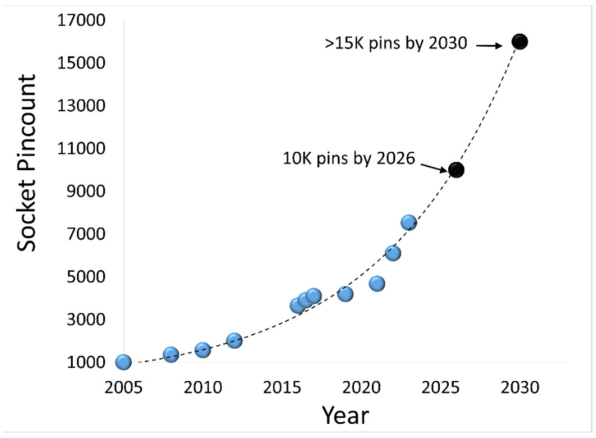
:1. Motivation
2. Interposer-Based ESD Protection for Chips in μ-Packaging
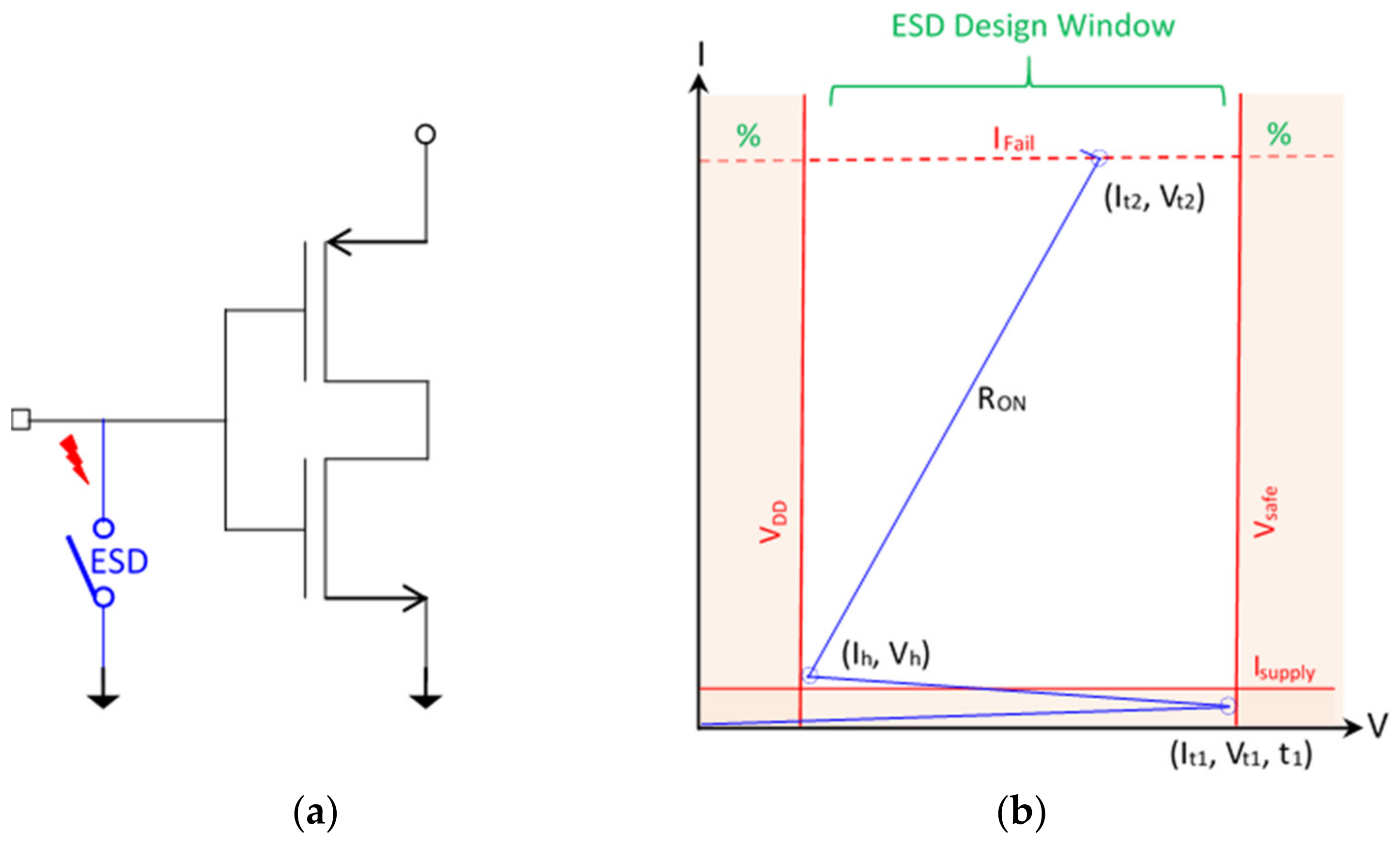
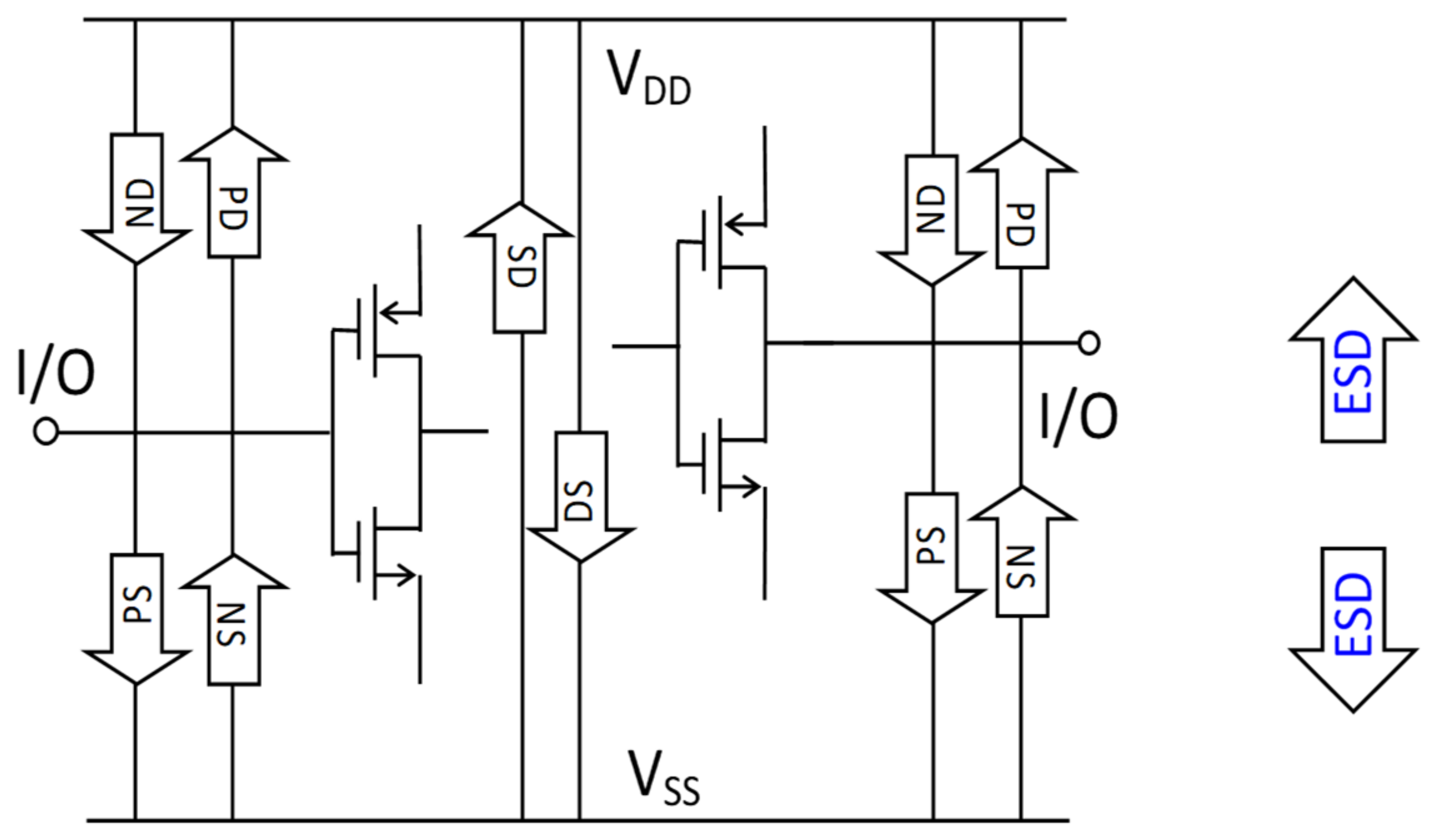
2.1. ESD Protection and Design Challenges
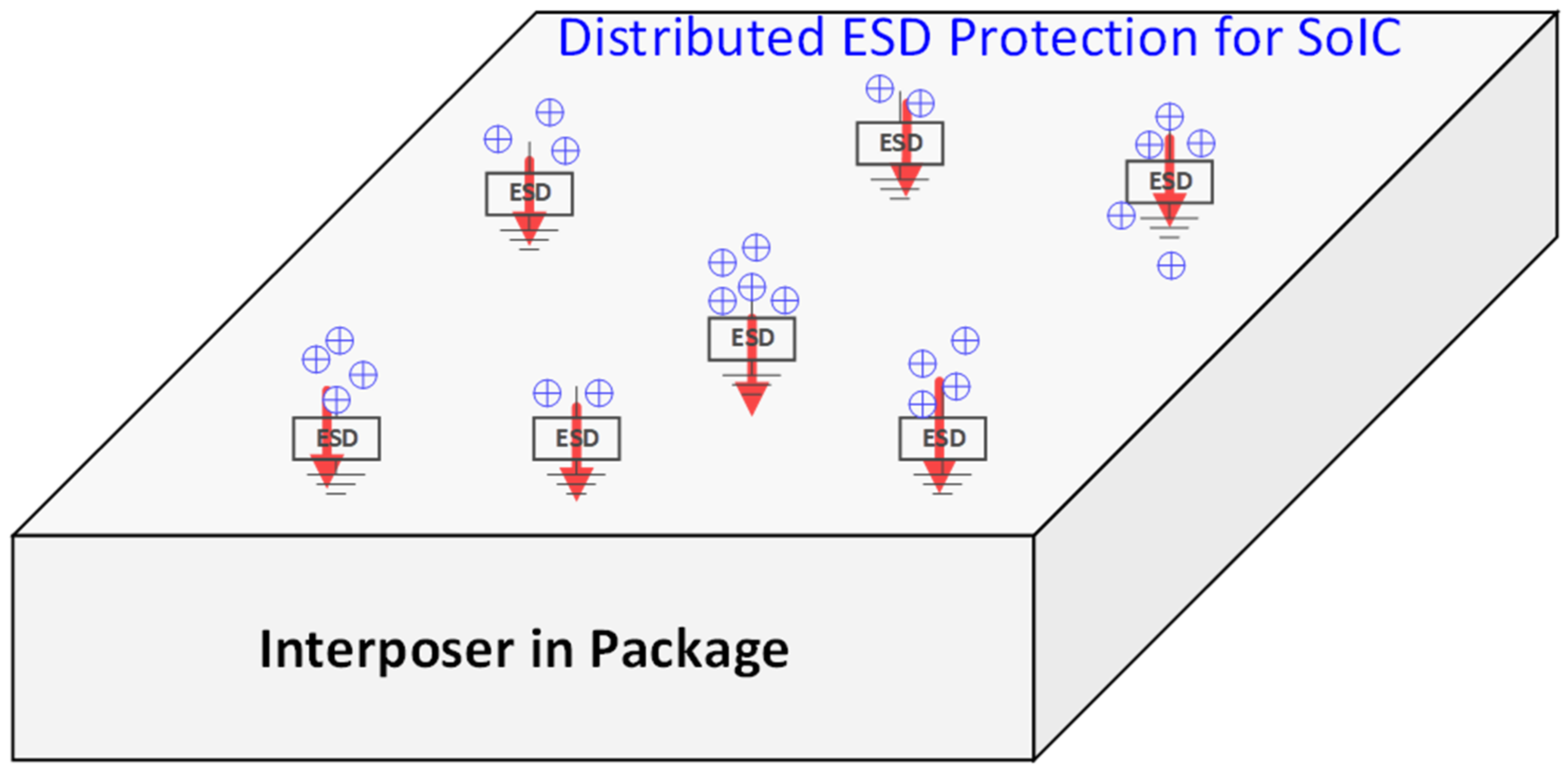
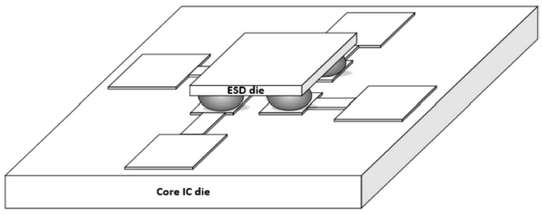
2.2. Novel Interposer-Based ESD Protection
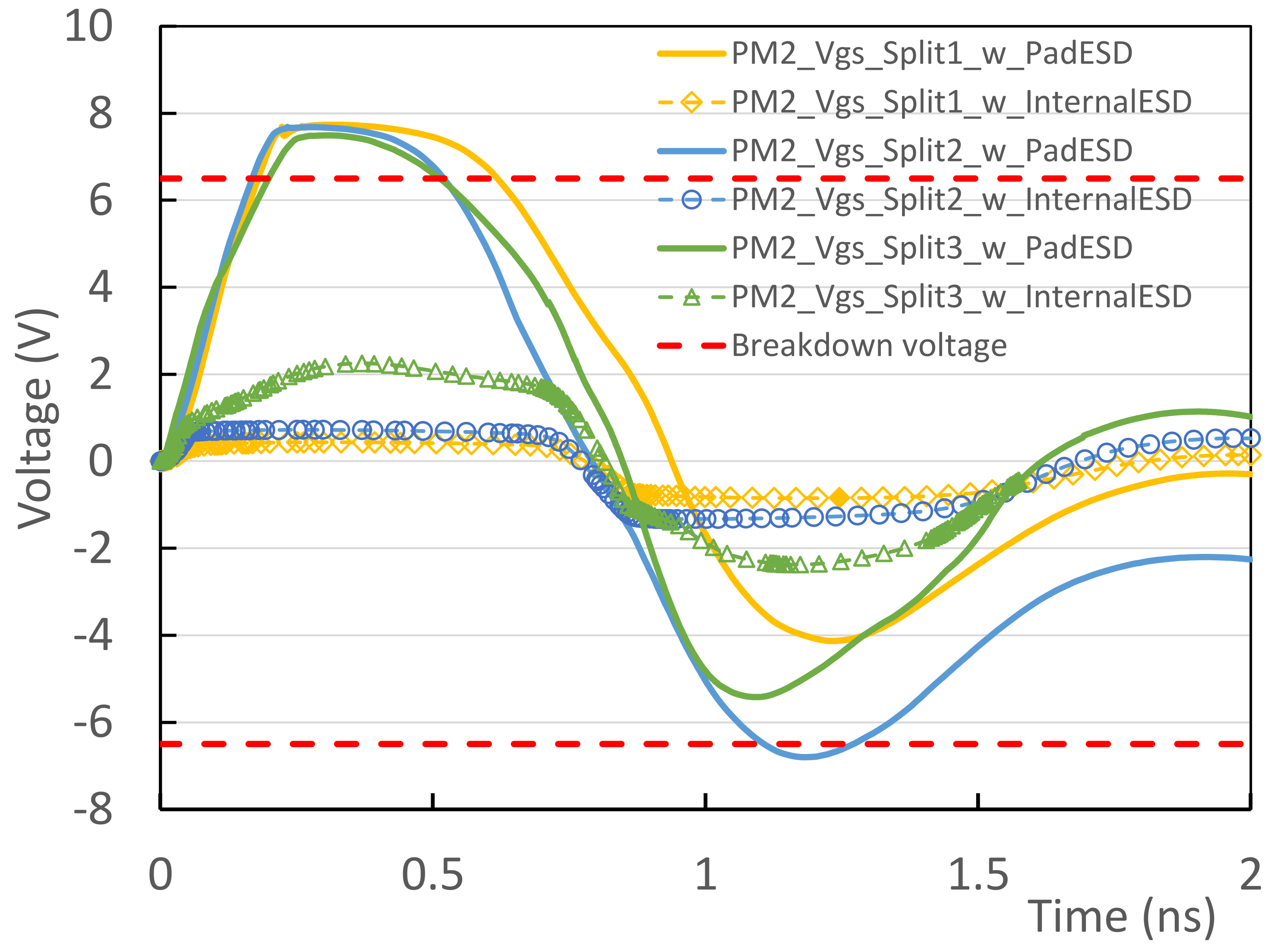
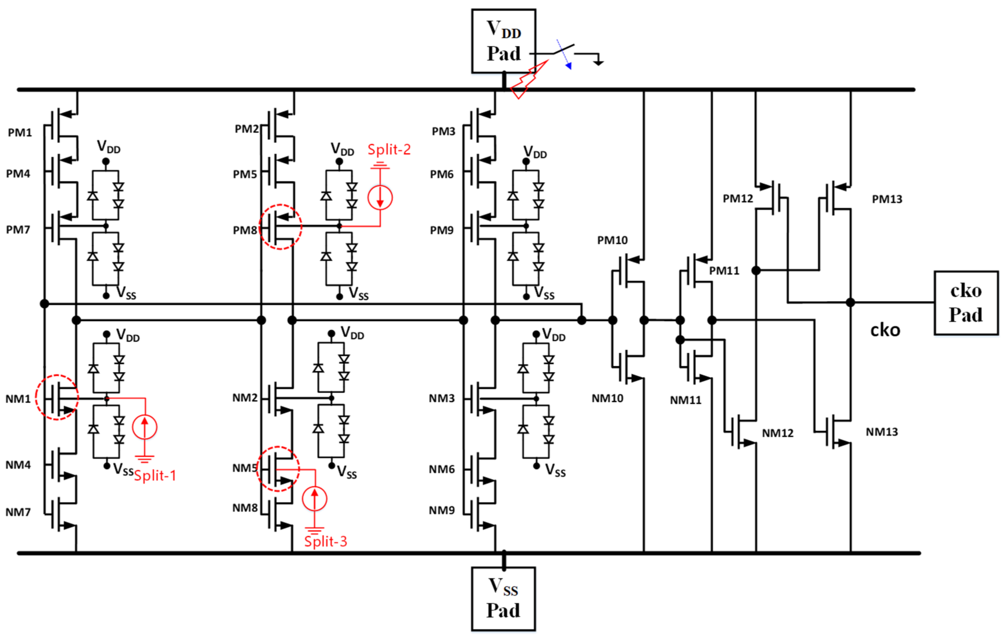
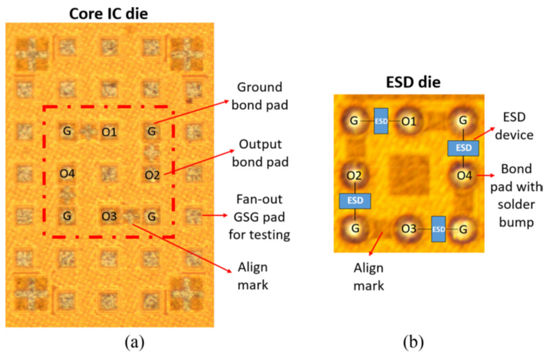
3. Proof of Concept Design Examples
4. Interposer-Based ESD Protection Design Challenges
5. Summary
6. Patents
Author Contributions
Funding
Data Availability Statement
Acknowledgments
Conflicts of Interest
Abbreviations
| CDM | Charged device model |
| CMOS | Complementary metal-oxide-semiconductor |
| ESD | Electrostatic discharge |
| HBM | Human body model |
| HI | Heterogeneous integration |
| IC | Integrated circuit |
| SoC | System-on-a-chip |
| SOI | Silicon-on-insulator |
| SoIC | Systems-on-integrated-chiplets |
References
- Brattain, W.H. Entry of 15 December 1947, Laboratory Notebook, Case 38139-7; Bell Laboratories Archives: Murray Hill, NJ, USA, 1947. [Google Scholar]
- Shockley, W. Circuit Element Utilizing Semiconductor Material. U.S. Patent 2,569,347A, 25 September 1951. [Google Scholar]
- Shockley, W. Semiconductor Amplifier. U.S. Patent 2,502,488A, 4 April 1950. [Google Scholar]
- Kilby, J.S. Miniaturized Electronic Circuits. U.S. Patent 3,138,743, 23 June 1964. [Google Scholar]
- Moore, G.E. Cramming more components onto integrated circuits. Electronics 1965, 38, 114–117. [Google Scholar] [CrossRef]
- IEEE Electronics Packaging Society. HIR: Heterogeneous Integration Roadmap, Edition 2024; IEEE Electronics Packaging Society: Piscataway, NJ, USA, 2024. Available online: https://eps.ieee.org/technology/heterogeneous-integration-roadmap/hir-special-sessions-at-estc-2024.html (accessed on 23 March 2025).
- Li, X.; Pan, Z.; Hao, W.; Miao, R.; Yue, Z.; Wang, A. Enhancing Chip Performance and Reliability by CMOS+X Technologies. Appl. Phys. Rev. 2024, 11, 021331. [Google Scholar] [CrossRef]
- CoWoS. TSMC. Available online: https://3dfabric.tsmc.com/english/dedicatedFoundry/technology/cowos.htm (accessed on 23 March 2025).
- Banijamali, B.; Chiu, C.-C.; Hsieh, C.-C.; Lin, T.-S.; Hu, C.; Hou, S.-Y.; Ramalingam, S.; Jeng, S.-P.; Madden, L.; Yu, D.C.H. Reliability evaluation of a CoWoS-enabled 3D IC package. In Proceedings of the IEEE 63rd Electronic Components and Technology Conference, Las Vegas, NV, USA, 28–31 May 2013; pp. 35–40. [Google Scholar]
- Pan, Z.; Li, X.; Hao, W.; Miao, R.; Wang, A. Design for EMI/ESD Immunity for Flexible and Wearable Electronics. IEEE J. Electron Devices Soc. (J-EDS) 2023, 11, 700–707. [Google Scholar] [CrossRef]
- Liang, S.W.; Liang, Y.R.; Wu, G.C.Y.; Yee, K.C.; Wang, C.T.; Yu, D.C.H. Reliability Performance on Fine-Pitch SoI Bond. In Proceedings of the IEEE Electronic Components and Technology Conference (ECTC), Orlando, FL, USA, 30 May–2 June 2023; pp. 783–787. [Google Scholar]
- Lu, R.; Chuang, Y.-C.; Wu, J.-L.; He, J. Reliability Challenges from 2.5D to 3DIC in Advanced Package Development. In Proceedings of the IEEE International Reliability Physics Symposium (IRPS), Monterey, CA, USA, 26–30 March 2023. [Google Scholar]
- Pan, Z.; Li, C.; Hao, W.; Li, X.; Wang, A. ESD Protection Designs: Topical Overview and Perspective. IEEE Trans. Device Mater. Reliab. (TDMR) 2022, 22, 356–370. [Google Scholar] [CrossRef]
- Wang, A. Practical ESD Protection Design; Wiley-IEEE Press: New York, NY, USA, 2022; ISBN 978-1119850403. [Google Scholar]
- Voldman, S. ESD: RF Technology and Circuits; Wiley: Hoboken, NJ, USA, 2006; ISBN-13: 978-0470847558. [Google Scholar]
- Semiconductor Market Size Worldwide by Application, ASML Via STATISTA, Yahoo!Finance. Available online: https://www.yahoo.com/finance/news/biden-has-big-plans-for-semiconductor-clusters--will-companies-play-along-200042981.html (accessed on 3 March 2023).
- Hao, W.; Pan, Z.; Li, X.; Miao, R.; Yue, Z.; Wang, A. On-Chip ESD Protection: Design Innovation. IEEE Electron Devices Rev. 2024, 2, 32–51. [Google Scholar] [CrossRef]
- Li, X.; Pan, Z.; Hao, W.; Miao, R.; Yue, Z.; Wang, A. On-Chip ESD Protection: Device Innovation. IEEE Electron Devices Rev. 2024, 1, 1–15. [Google Scholar] [CrossRef]
- Pan, Z.; Li, X.; Hao, W.; Miao, R.; Wang, A. On-Chip ESD Protection Design Methodologies by CAD Simulation. ACM Trans. Des. Autom. Electron. Syst. (TODAES) 2023, 29, 1–41. [Google Scholar] [CrossRef]
- Di, M.; Pan, Z.; Zhang, F.; Li, C.; Wang, H.; Wang, A. A Study of ESD-mmWave-Switch Co-Design of 28GHz Distributed Travelling Wave Switch in 22nm FDSOI for 5G Systems. IEEE J. Electron Devices Soc. (J-EDS) 2021, 6, 1290–1296. [Google Scholar] [CrossRef]
- IEEE Electronics Packaging Society. Chapter 22: Interconnects for 2D and 3D Architectures. In HIR: Heterogeneous Integration Roadmap, Edition 2024; IEEE Electronics Packaging Society: Piscataway, NJ, USA, 2024. [Google Scholar]
- Knickerbocker, J.U.; Andry, P.S.; Dang, B.; Horton, R.R.; Patel, C.S.; Polastre, R.J.; Sakuma, K.; Sprogis, E.S.; Tsang, C.K.; Webb, B.C.; et al. 3D silicon integration. In Proceedings of the Electronic Components and Technology Conference (ECTC), Lake Buena Vista, FL, USA, 27–30 May 2008; pp. 538–543. [Google Scholar]
- Ogutu, P.; Fey, E.; Dimitrov, N. Superconformal filling of high aspect ratio through glass vias (TGV) for interposer applications using TNBT and NTBC additives. J. Electrochem. Soc. 2015, 162, D457. [Google Scholar] [CrossRef]
- Hamelink, J.; Poelma, R.H.; Kengen, M. Through-polymer-via for 3D heterogeneous integration and packaging. In Proceedings of the IEEE 17th Electronics Packaging and Technology Conference (EPTC), Singapore, 2–4 December 2015; pp. 1–7. [Google Scholar]
- Martwick, A.; Drew, J. Silicon Interposer and TSV Signaling. In Proceedings of the IEEE 65th Electronic Components and Technology Conference (ECTC), San Diego, CA, USA, 26–29 May 2015; pp. 266–275. [Google Scholar]
- Zaghari, P.; Sinha, S.S.; Hopkins, D.C.; Ryu, J.E. Co-Design and ML-Based Optimization of Through-Via in Silicon and Glass Interposers for Electronic Packaging Applications. IEEE Trans. Compon. Manuf. Technol. 2025, 15, 295–308. [Google Scholar] [CrossRef]
- Cai, M.; Ling, B.; Chen, D.; Xia, Y.; Wang, H.; Han, Y.; Wu, Y. Double-layer-stacked Silicon Interposer for 2.5D Packaging of 32 × 32 Micromirror Array Chip. IEEE Trans. Compon. Packag. Manuf. Technol. 2025, 15, 706–715. [Google Scholar] [CrossRef]
- Kim, J. Active Si Interposer for 3D IC Integrations. In Proceedings of the 2015 International 3D Systems Integration Conference (3DIC), Sendai, Japan, 31 August–2 September 2025. [Google Scholar]
- Liu, Y.; Li, D.; Yang, Z.; Zhang, C.; Zhang, Y.; Li, X.; Cao, M.; Yin, S. A Chiplet Platform for Intelligent Radar/Sonar Leveraging Domain-Specific Reusable Active Interposer. IEEE. Trans. Very Large Scale Integr. 2025, 33, 903–915. [Google Scholar] [CrossRef]
- Jiao, B.; Zhu, H.; Zeng, Y.; Li, Y.; Liao, J.; Jia, S.; Chen, Z.; Tian, M.; Zhu, J.; Wen, D.; et al. 37.4 SHINAI: A 586 mm2 Reusable Active TSV Interposer with Programmable Interconnect Fabric and 512 Mb 3D Underdeck Memory. In Proceedings of the 2025 IEEE International Solid-State Circuits Conference (ISSCC), San Francisco, CA, USA, 16–20 February 2025. [Google Scholar]
- Jayabalan, J.; Chidambaram, V.; Siang, S.L.P.; Wang, X.; Chinq, J.M.; Bhattacharya, S. Active Through-Silicon Interposer Based 2.5D IC Design, Fabrication, Assembly and Test. In Proceedings of the IEEE 69th Electronic Components and Technology Conference (ECTC), Las Vegas, NV, USA, 28–31 May 2019; pp. 587–593. [Google Scholar]
- Industry Council on ESD Target Levels. White Paper 1: A Case for Lowering Component Level HBM ESD Specifications and Requirements, Industry Council on ESD Target Levels, Rev. 4.0; Industry Council on ESD Target Levels: Online, 2018. [Google Scholar]
- Industry Council on ESD Target Levels. White Paper 2: A Case for Lowering Component-Level CDM ESD Specifications and Requirements, Industry Council on ESD Target Levels, Rev. 3.0; Industry Council on ESD Target Levels: Online, 2021. [Google Scholar]
- Di, M.; Li, C.; Pan, Z.; Wang, A. Pad-Based CDM ESD Protection Methods Are Faulty. IEEE J. Electron Devices Soc. (J-EDS) 2020, 8, 1297–1304. [Google Scholar] [CrossRef]
- ANSI/ESDA/JEDEC JS-001-2017; For Electrostatic Discharge Sensitivity Testing—Human Body Model (HBM)—Component Level. ESD Association: Rome, NY, USA; JEDEC: Arlington, VA, USA, 2017.
- ANSI/ESDA/JEDEC JS-002-2018; For Electrostatic Discharge Sensitivity Testing—Charged Device Model (CDM)—Device Level. ESD Association: Rome, NY, USA; JEDEC: Arlington, VA, USA, 2018.
- Di, M.; Li, C.; Pan, Z.; Wang, A. Non-Pad-Based in Situ in-Operando CDM ESD Protection Using Internally Distributed Network. IEEE J. Electron Devices Soc. (J-EDS) 2021, 9, 1248–1256. [Google Scholar] [CrossRef]
- Wang, A. Interposer-Based ESD Protection Structures. U.S. Patent 62/412,105, 25 October 2016. [Google Scholar]
- Li, C.; Di, M.; Pan, Z.; Wu, H.; Wang, A. Vertical TSV-Like Diode ESD Protection. In Proceedings of the IEEE Electron Devices Technology and Manufacturing Conference (EDTM), Chengdu, China, 9–12 March 2021; pp. 676–678. [Google Scholar]


Disclaimer/Publisher’s Note: The statements, opinions and data contained in all publications are solely those of the individual author(s) and contributor(s) and not of MDPI and/or the editor(s). MDPI and/or the editor(s) disclaim responsibility for any injury to people or property resulting from any ideas, methods, instructions or products referred to in the content. |
© 2025 by the authors. Licensee MDPI, Basel, Switzerland. This article is an open access article distributed under the terms and conditions of the Creative Commons Attribution (CC BY) license (https://creativecommons.org/licenses/by/4.0/).
Share and Cite
Li, X.; Pan, Z.; Hao, W.; Miao, R.; Yue, Z.; Wang, A. Interposer-Based ESD Protection: A Potential Solution for μ-Packaging Reliability of 3D Chips. Micromachines 2025, 16, 488. https://doi.org/10.3390/mi16040488
Li X, Pan Z, Hao W, Miao R, Yue Z, Wang A. Interposer-Based ESD Protection: A Potential Solution for μ-Packaging Reliability of 3D Chips. Micromachines. 2025; 16(4):488. https://doi.org/10.3390/mi16040488
Chicago/Turabian StyleLi, Xunyu, Zijin Pan, Weiquan Hao, Runyu Miao, Zijian Yue, and Albert Wang. 2025. "Interposer-Based ESD Protection: A Potential Solution for μ-Packaging Reliability of 3D Chips" Micromachines 16, no. 4: 488. https://doi.org/10.3390/mi16040488
APA StyleLi, X., Pan, Z., Hao, W., Miao, R., Yue, Z., & Wang, A. (2025). Interposer-Based ESD Protection: A Potential Solution for μ-Packaging Reliability of 3D Chips. Micromachines, 16(4), 488. https://doi.org/10.3390/mi16040488