Abstract
This paper proposes a 1200V 4H-SiC MOSFET incorporating a High-K dielectric-integrated fused source-gate (HKSG) structure, engineered to concurrently enhance the third-quadrant operation and high-frequency figure of merit (HF-FOM). The High-K dielectric enhances the electric field effect, reducing the threshold voltage of the source-gate. As a result, the reverse conduction voltage drops from 2.79 V (body diode) to 1.53 V, and the bipolar degradation is eliminated. Moreover, by incorporating a shielding area within the merged source-gate architecture, the gate-to-drain capacitance Cgd of the HKSG-MOS is reduced. The simulation results show that the HF-FOM Cgd × Ron,sp and Qgd × Ron,sp of the HKSG-MOS are decreased by 48.1% and 58.9%, respectively, compared with that of conventional SiC MOSFET. The improved performances make the proposed SiC MOSFEET have great potential in high-frequency power applications.
1. Introduction
Silicon carbide (SiC) MOSFETs have emerged as prominent power devices due to their superior characteristics, including a wide bandgap, high critical breakdown electric field, high current density, and excellent thermal conductivity. These attributes surpass traditional silicon materials, making SiC MOSFETs ideal for applications in automobiles, intelligent power systems, national defense, and aerospace [1,2,3,4].
In power electronics, the conventional use of anti-parallel diodes to sustain inductor currents persists, but the direct use of SiC MOSFETs’ parasitic body diode risks bipolar degradation, impacting on-resistance and blocking capabilities [5,6]. To elevate power density and mitigate this, researchers are exploring innovations within SiC MOSFET cells. Studies [1,7,8,9] propose integrating Schottky Barrier Diodes (SBDs) into SiC MOSFETs, offering cost, space, and efficiency benefits. However, the semiconductor–metal interface may have molecular discontinuities, leading to irregularities, defects, and leakage currents under strong electric fields. Alternatively, research [10,11,12,13] introduces SiC MOSFETs with Low-Barrier Diodes (LBDs), enabling low-voltage reverse conduction due to channel depletion. To further optimize performance, an LBD combined with a source-gate (SG) structure has emerged [12,14]. The SG [15,16] structure significantly improves the third-quadrant performance of the device by forming an inversion layer, while its gate-shielding effect further optimizes the high-frequency figure of merit (HF-FOM). To enhance dynamic characteristics such as HF-FOM, researchers have also explored heterojunction-based approaches [17,18]. Nevertheless, these methods introduce interfacial defects and reliability concerns due to lattice mismatch and high interface trap densities. Both strategies—SG and heterojunction designs—suffer from intricate fabrication processes and elevated costs, limiting their practical implementation.
This paper proposes a fused source gate integrated with High-K dielectric (HKSG) MOSFET structure [19,20,21,22,23]. This structure employs a simplified source-gate design to control the N-type channel, incorporating a high-k dielectric material as the gate dielectric to optimize third-quadrant characteristics. When the source gate is connected, it effectively shields one side of the gate’s electric field. As a result, the effective facing area of the gate oxide capacitance is reduced, which, in turn, decreases the gate-to-drain capacitance (Cgd). This combined design not only decreases the device’s capacitance but also significantly cuts down the high-frequency figure of merit Cgd × Ron,sp and Qgd × Ron,sp. Compared with traditional multi-gate structures, it shows remarkable advantages.
2. Device Structure and Mechanism
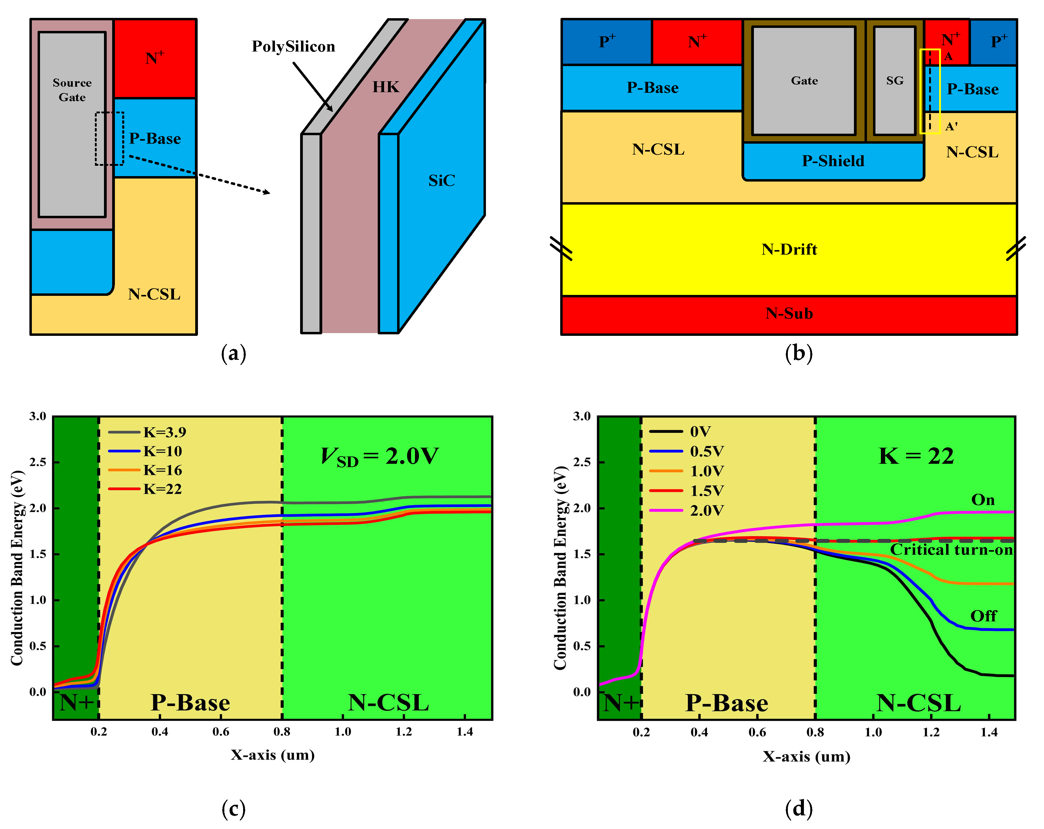
Figure 1a–c present the schematic cross-sectional configurations of the conventional SiC MOSFET (CON-MOS), the source-gate MOSFET (SG-MOS) and the proposed High-K source-gate MOSFET (HKSG-MOS), respectively. As shown in Figure 1c, the HKSG-MOS introduces an additional channel on the right side of the device. The channel is controlled by the source gate. Moreover, the silica dielectric surrounding the source gate is replaced by the high-k material. The incorporation of the high-k dielectric significantly lowers the threshold voltage compared to the turn-on voltage of the MOS parasitic diode.
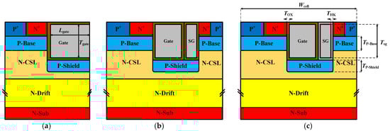
Figure 1.
Schematic cross-sectional view of (a) Con-MOS, (b) SG-MOS, and (c) HKSG-MOS.
To better understand the impact of the SG on reverse conduction characteristics, the structure can be simplified into a metal–insulator–semiconductor (MIS) parallel plate capacitor, as shown in Figure 2a. As the dielectric constant of the material increases, the capacitance of the parallel plate capacitor will increase, allowing more electrons to accumulate under the same voltage, thereby lowering the threshold voltage. Figure 2b shows the cross-sectional view of the proposed structure with the line A-A′. To understand the operating mechanism of the device during reverse conduction, it is crucial to clarify the conduction band energy distribution in the region where line A-A′ is located. Figure 2c shows the conduction band energy (EC) along line A-A′ with different K values at VSD = 2.0 V. As can be seen in Figure 2c, the EC decreases with an increase in K value. As a result, the reverse conduction voltage is decreased. Figure 2d shows EC along line A–A′ with different source-to-drain voltages (VSD) when K = 22. The EC at the N-CSL region increases with sn increase in VSD. Once the electron energy is higher than the potential barrier (VSD = 1.5 V), the electrons in the N-CSL region could flow through the P-Base to the N+ region. Therefore, unipolar conduction in the MOS channel begins, which eliminates bipolar degradation and improves the reliability of the device.
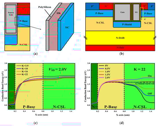
Figure 2.
Schematic view of (a) the simplified mezzanine plate capacitors. (b) Cross-sectional view along with line A–A′. (c) Conduction band energy distribution along A–A′ cut-line at different K values. (d) Conduction band energy distribution along A–A′ cut-line at different VSD values.
In order to investigate the characteristics of the proposed structure, 2D numerical simulations were performed by Sentaurus TCAD 2022 [24]. The physical models in the simulation mainly include Aniso (Mobility Valanche), effective intrinsic density (Old Slotboom), mobility (Incomplete Ionization High-Field-Saturation Enormal), and recombination (Shockley–Read–Hall Doping Dep Auger Avalanche). Detailed parameters used in the simulation are shown in Table 1.

Table 1.
Detailed parameters used in simulation.
3. Simulation Results and Discussion
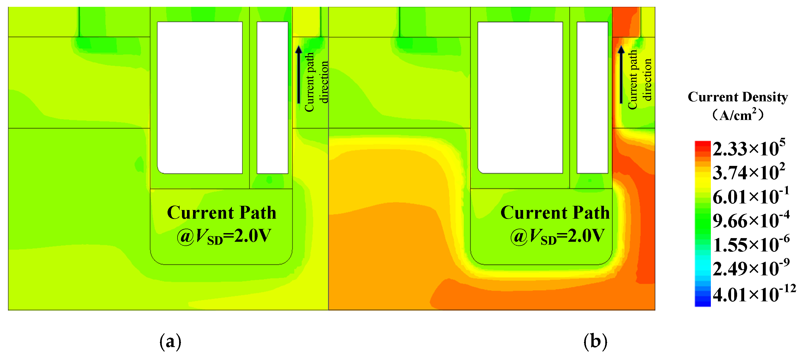
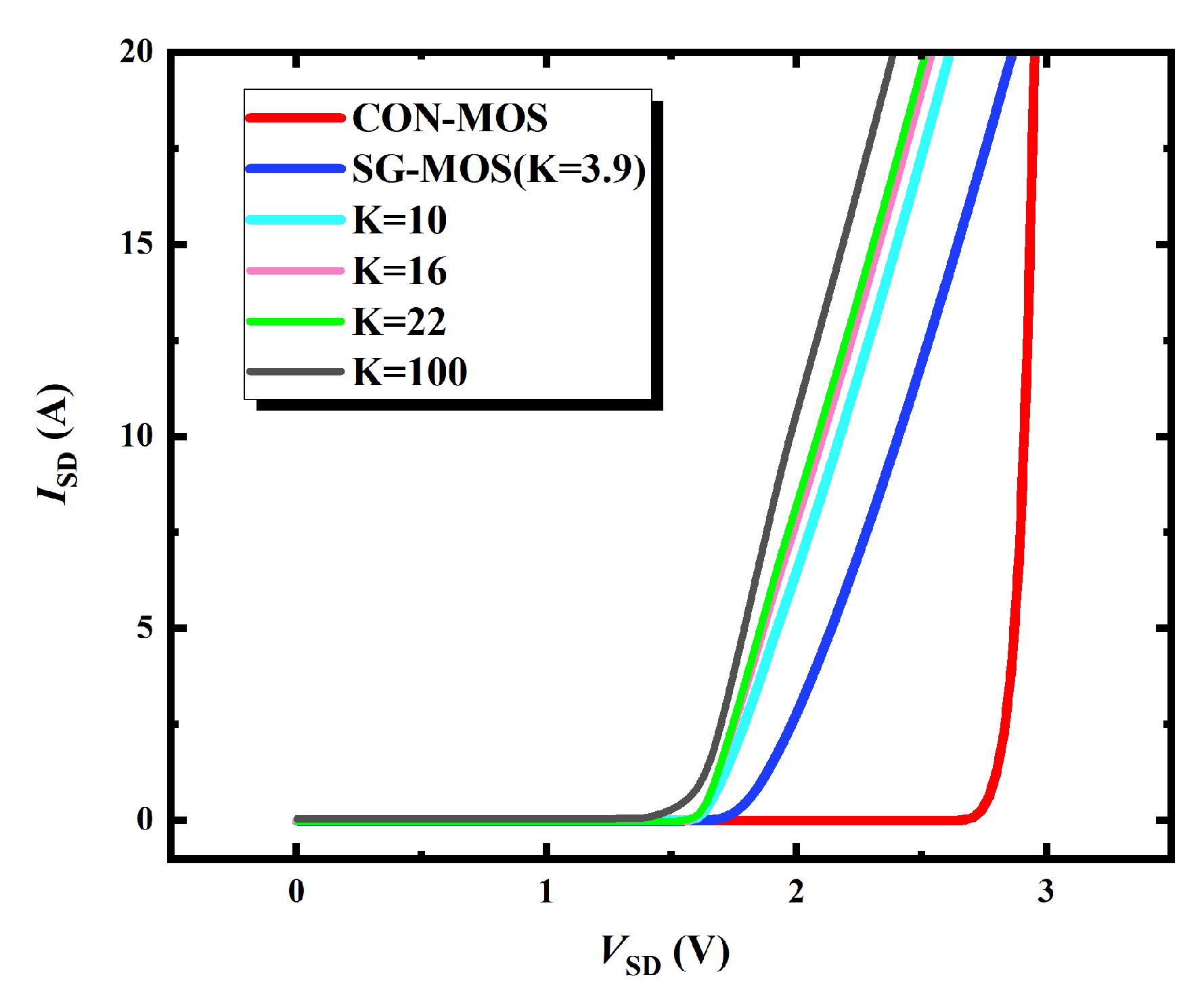
Figure 3 gives the reverse conduction characteristics of SG-MOS and HKSG-MOS at VSD = 3 V. Figure 3 indicates that the third-quadrant conduction current predominantly concentrates beneath the right-side SG, thereby effectively suppressing the body diode activation and avoiding bipolar degradation. Moreover, due to the introduced high-k dielectric, the reverse conduction voltage of HKSG-MOS is reduced compared with that of SG-MOS. Figure 4 shows that, when the K values increase from 3.9 to 100, the reverse conduction voltage decreases from 1.65 V to 1.41 V. More than that, the enhanced electron concentration induced by the HKSG leads to a significant increase in the third-quadrant current. As can be seen from Figure 4, the reverse current increases from 2.75 A (K = 3.9) to 10.51 A (K = 100) at VSD = 2.0 V. Figure 4 also indicates that, due to third-quadrant unipolar conduction, the reverse Von of HKSG-MOS is decreased by 49.46% compared with that of CON-MOS.
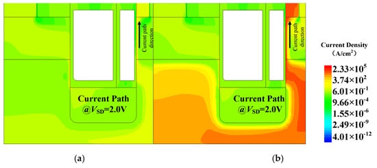
Figure 3.
Schematic diagram of reverse conduction current path: (a) SG-MOS; (b) HKSG-MOS.
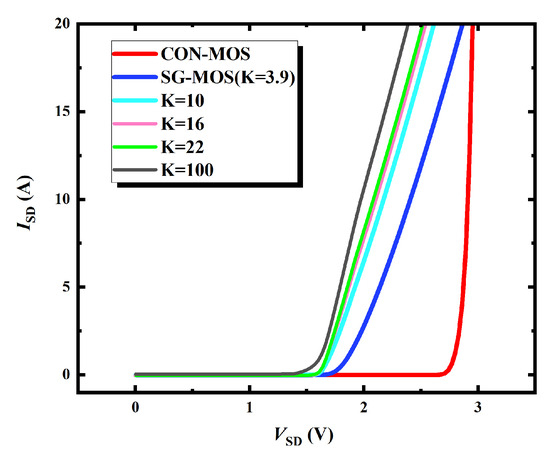
Figure 4.
Reverse conduction I-V curves of CON-MOS, SG-MOS, and HKSG-MOS.
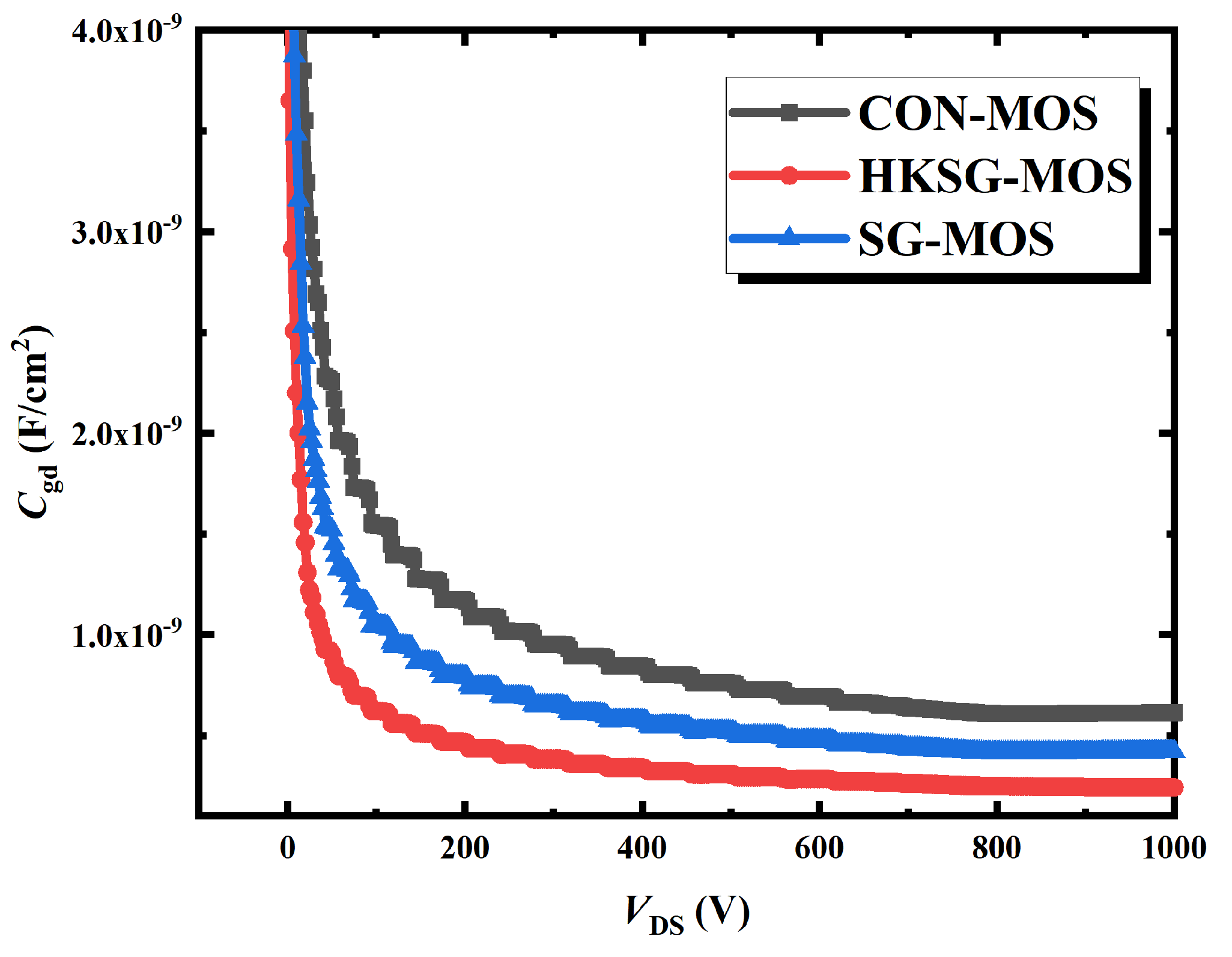
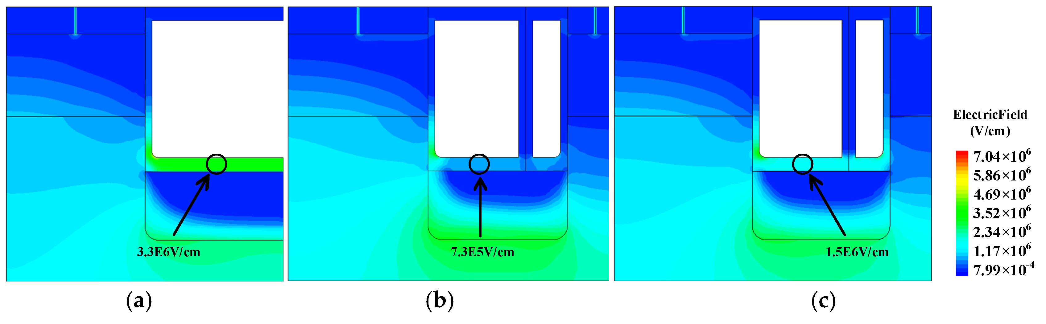
The gate-to-drain capacitance (Cgd) of conventional MOS, SG-MOS, and HKSG-MOS are illustrated in Figure 5. The Cgd extracted at VDS = 800 V is 607.84, 415.75, and 248.02 pF/cm2 for CON-MOS, SG-MOS, and HKSG-MOS, respectively. Because of the weakened electric field distribution in the dielectric (labeled in Figure 6), the Cgd of the HKSG-MOS is reduced. Figure 6 shows the 2D electric field distributions of CON-MOS, SG-MOS, and HKSG-MOS. As can be seen in Figure 6, a portion of the gate-directed electric field lines are redistributed to the source-side SG, thereby reducing the Cgd, with this shielding effect becoming more pronounced at higher K values. Therefore, the Cgd of the HKSG-MOS is the smallest among these structures.
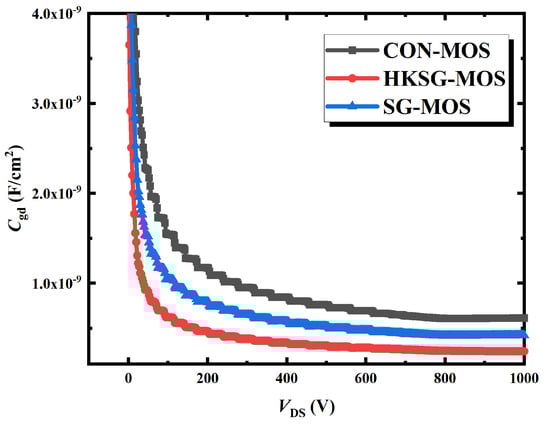
Figure 5.
The gate-to-drain capacitance C-V characteristics of CON-MOS, SG-MOS, and HKSG-MOS.
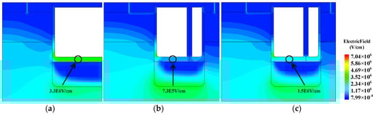
Figure 6.
Electric field distributions of (a) CON-MOS, (b) SG-MOS, and (c) HKSG-MOS.
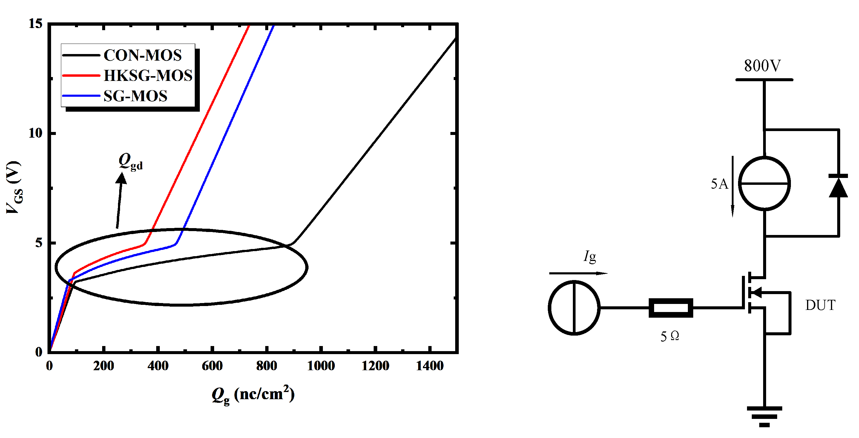
Figure 7 shows the gate charge characteristics of CON-MOS, SG-MOS, and HKSG-MOS. As with the reduction in the Cgd, the Qgd of HKSG-MOS is reduced by 67.71% and 34.67%, respectively, compared to the CON-MOS and SG-MOS. Consequently, owing to the significantly reduced Cgd and Qgd, the high-frequency figures of merit HF-FOM1 (Ron,sp × Cgd) of the HKSG-MOS are reduced by 48.15% and 34.23% compared to CON-MOS and SG-MOS, respectively. The high-frequency figures of merit HF-FOM2 (Ron,sp × Qgd) of the HKSG-MOS are reduced by 58.97% and 27.98% compared to CON-MOS and SG-MOS, respectively.
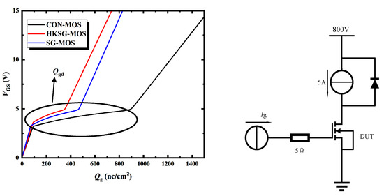
Figure 7.
Gate charge characteristics of CON-MOS, SG-MOS, and HKSG-MOS.
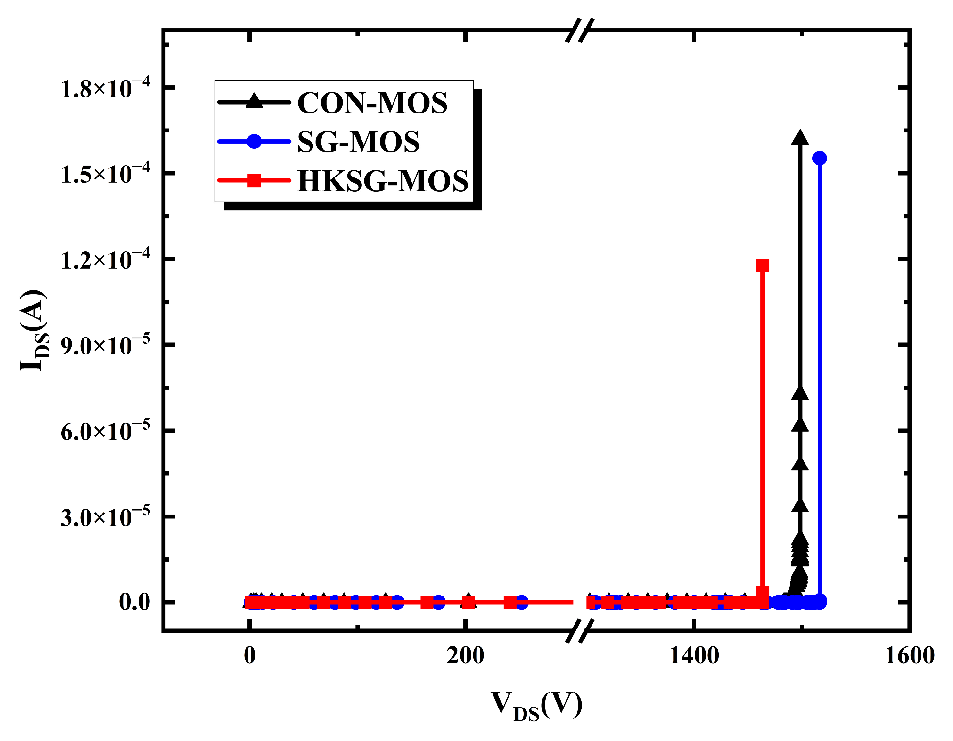
As depicted in Figure 8, the breakdown voltages (BVs) of the CON-MOS, SG-MOS, and HKSG-MOS are 1498 V, 1516 V, and 1463 V, respectively. The slight differences in the BV of the three structures are due to the varying K value of the SG dielectric, which slightly affects the electric field strength in the right corner of the P-Shield region.
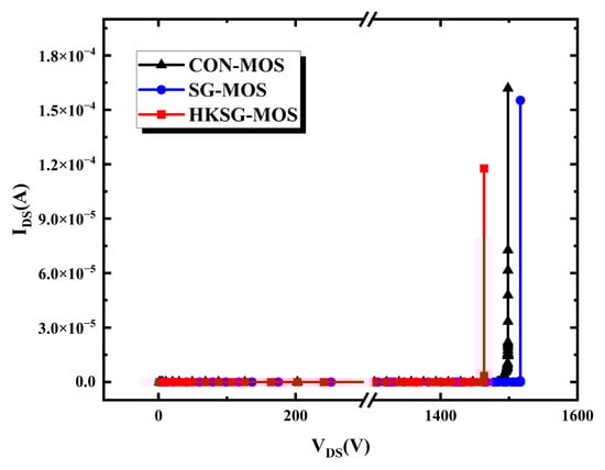
Figure 8.
The forward blocking characteristic of CON-MOS, SG-MOS, and HKSG-MOS.
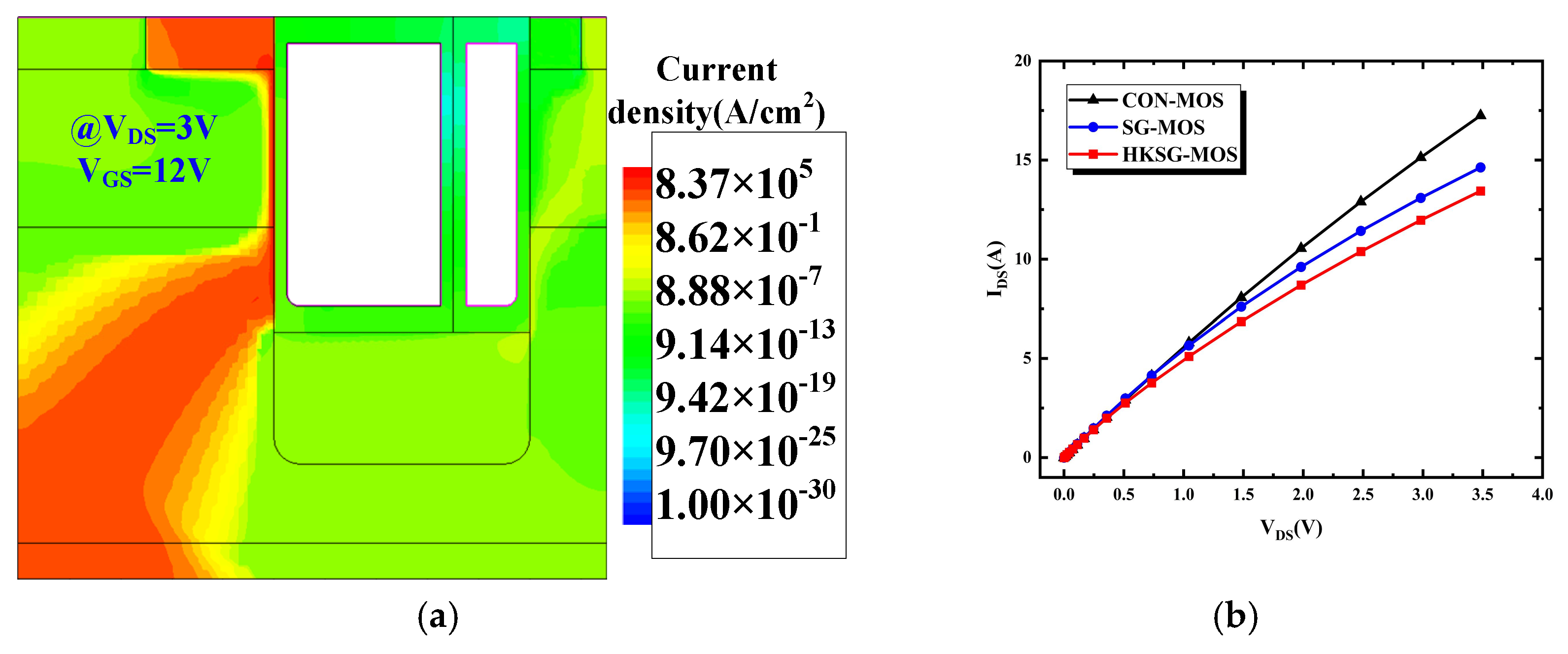
Figure 9 shows the forward conduction characteristic of CON-MOS, SG-MOS, and HKSG-MOS. Figure 9a indicates that the forward conduction current predominantly concentrates beneath the gate at the left side of HKSG-MOS. Owing to the modulated bulk electric field by the SG, the width of the current path is narrowed, resulting in an increased Ron,sp for HKSG-MOS. Figure 9b shows the forward conduction I–V curves of CON-MOS, SG-MOS, and HKSG-MOS at VGS = 12 V. When VDS = 1 V, the calculated specific on-resistance (Ron,sp) values for CON-MOS, SG-MOS, and HKSG-MOS are 1.44 mΩ·cm2, 1.66 mΩ·cm2, and 1.83 mΩ·cm2, respectively.
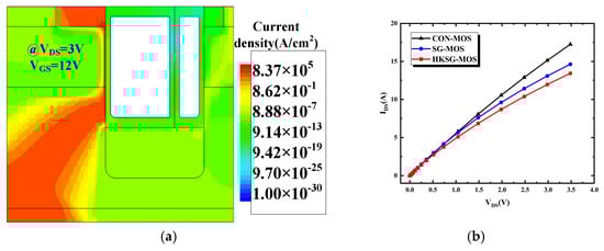
Figure 9.
Schematic view of (a) the forward conduction current distributions of the HKSG-MOS and (b) the forward I–V curves of CON-MOS, SG-MOS, and HKSG-MOS.
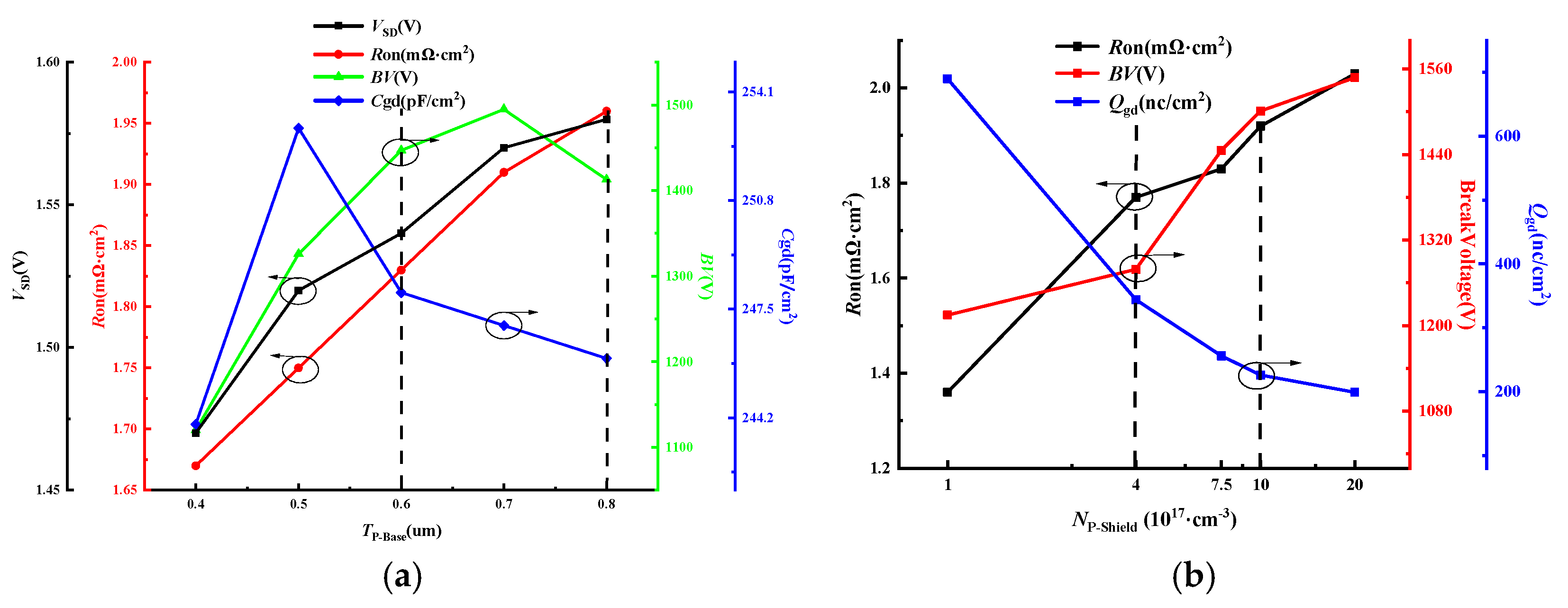
Figure 10 shows the influence of the P-base depth (TP-Base) and the concentration of the P-shield (NP-Shield) on the HKSG-MOS. While the TP-Base is increasing, the Cgd will increase first for the increasement of the electric field besides the oxide gate and finally reduced for the decrease in the effective capacitor area. Meanwhile, the BV will increase for the longer channel and finally decrease for the increasement of the electric field. Both of the VSD and the Ron will increase for the channel length. The NP-Shield mainly controls the electric field distribution around the gate and the channel. As a result, the enhanced JFET effect increases the Ron and improves the BV. The Qgd is reduced by the electric field shielding. Table 2 compares the main characteristics of CON-MOS, SG-MOS, and HKSG-MOS.
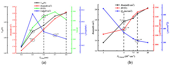
Figure 10.
Influence of the P-base depth (TP-Base) and the concentration of the P-shield (NP-Shield) on the HKSG-MOS. (a) the P-base depth TP-Base. (b) the concentration of the P-shield NP-Shield.
Table 2.
Simulated device electrical parameters.
Figure 11 shows the switch characteristics of HKSG-MOS and Con-MOS. Due to the decrease in the Cgd, the dv/dt of HKSG-MOS is sharper than Con-MOS. The increase in Cgs leads to an earlier turning on of Con-MOS. The unipolar reverse conduction model reduces the reverse recovery current, which improves the turn-on loss by 50.7% (HKSG-MOS: 3.56 mJ/cm2; Con-MOS: 7.22 mJ/cm2). The turn-off loss of HKSG-MOS and Con-MOS are 3.05 mJ/cm2 and 5.47 mJ/cm2, respectively. The lower Cgd of HKSG-MOS makes the turn-off process faster and reduces the loss.
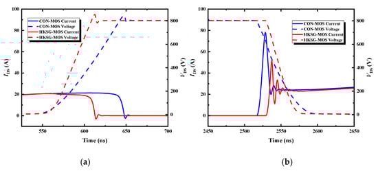
Figure 11.
Switch characteristics of HKSG-MOS and Con-MOS. (a) Turn-off process. (b) Turn-off process.
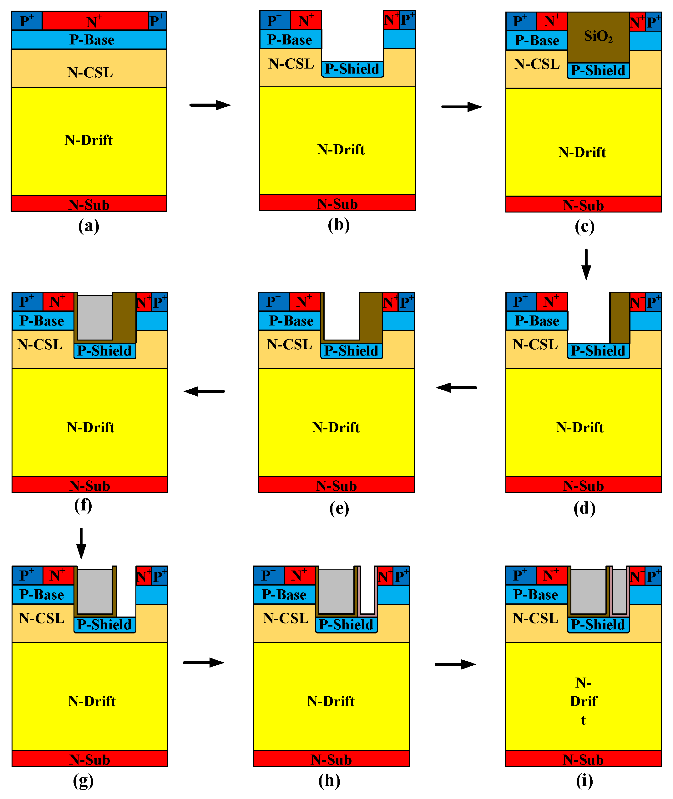
The process flow is illustrated in Figure 12. Considering the isolation issue between the gate and HKSG, a two-step etching scheme was adopted in this paper to fabricate the trench gate. First, deposit SiO2 to form the isolation between the gate and HKSG. Second, etch the gate trench and form the gate oxide by oxidation. After the gate fabrication process, the second etch process is adopted to form a HKSG trench, which leaves a thick enough SiO2 wall to isolate the gate and HKSG.
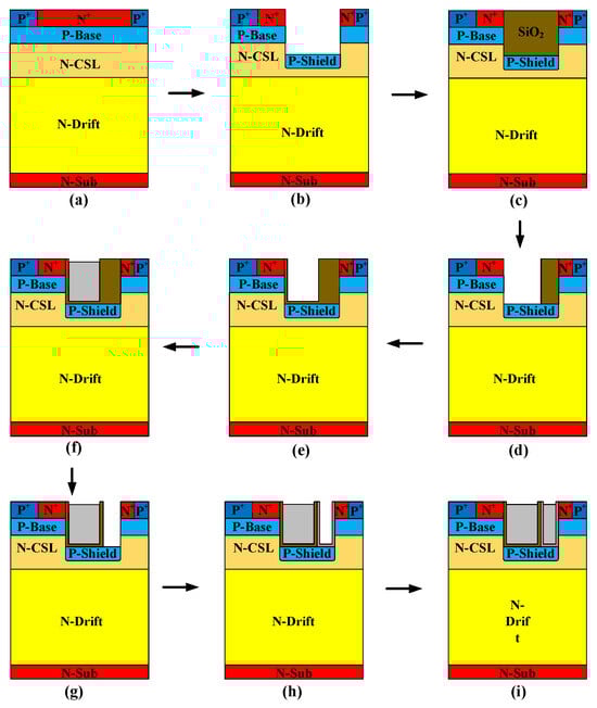
Figure 12.
Brief fabrication process flow of HKSG-MOS. (a) Epitaxial growth of N-CSL and ion implantation of P-base, P+ and N+ region. (b) Trench etching and P-shield implantation. (c) SiO2 deposition. (d) Gate etching. (e) Gate oxidation. (f) Poly silicon deposition. (g) HK gate etching. (h) HK formation. (i) Poly silicon deposition.
4. Conclusions
A 1200V 4H-SiC MOSFET incorporating a High-K dielectric-integrated fused source-gate (HKSG) structure is proposed in this paper. The results demonstrate that the HKSG-MOS achieves a substantially lower reverse conduction voltage (1.41 V vs. 2.79 V) while simultaneously providing a unipolar current path. Notably, by incorporating a shielding area within the merged source-gate architecture, the HFFOM Cgd × Ron,sp and Qgd × Ron,sp of the HKSG-MOS are decreased by 48.1% and 58.9%, respectively, compared with that of conventional SiC MOSFET. These findings conclusively establish HKSG-MOS as a highly competitive candidate for high-power and high-frequency applications.
Author Contributions
Conceptualization, M.L. and Y.K.; methodology, Z.Q.; software, T.L.; validation, M.L., Z.Q. and T.L.; formal analysis, Z.Q.; investigation, M.L.; resources, X.H.; writing—original draft preparation, M.L.; writing—review and editing, S.L.; supervision, X.H. All authors have read and agreed to the published version of the manuscript.
Funding
This research was funded by [Analysis and optimization of semiconductor device] grant number [RH2400005673].
Data Availability Statement
The original contributions presented in the study are included in the article, further inquiries can be directed to the corresponding author.
Conflicts of Interest
The authors declare no conflict of interest.
References
- Tang, L.; Jiang, H.; Wei, J.; Hu, Q.; Zhong, X.; Qi, X. A comparative study of SiC MOSFETs with and without integrated SBD. Microelectron. J. 2022, 128, 105576. [Google Scholar] [CrossRef]
- Liu, S.; Huang, M.; Wang, M.; Zhang, M.; Wei, J. Considerations for SiC super junction MOSFET: On-resistance, gate structure, and oxide shield. Microelectron. J. 2023, 137, 105823. [Google Scholar] [CrossRef]
- Kong, M.; Duan, Y.; Zhang, B.; Yan, R.; Yi, B.; Yang, H. A novel 4H-SiC accumulation mode MOSFET with ultra-low specific on-resistance and improved reverse recovery capability. IET Power Electron. 2023, 16, 2369–2377. [Google Scholar] [CrossRef]
- Wei, J.; Jiang, Q.; Luo, X.; Huang, J.; Yang, K.; Ma, Z.; Fang, J.; Yang, F. High performance SiC trench-type MOSFET with an integrated MOS-channel diode. Chin. Phys. B 2023, 32, 028503. [Google Scholar] [CrossRef]
- Luo, X.; Zhang, K.; Song, X.; Fang, J.; Yang, F.; Zhang, B. 4H-SiC trench MOSFET with an integrated Schottky barrier diode and L-shaped P+ shielding region. J. Semicond. 2020, 41, 102801. [Google Scholar] [CrossRef]
- Ishigaki, T.; Murata, T.; Kinoshita, K.; Morikawa, T.; Oda, T.; Fujita, R.; Konishi, K.; Mori, Y.; Shima, A. Analysis of Degradation Phenomena in Bipolar Degradation Screening Process for SiC MOSFETs. In Proceedings of the 2019 31st International Symposium on Power Semiconductor Devices and ICs, Shanghai, China, 19–23 May 2019; pp. 259–262. [Google Scholar] [CrossRef]
- Aiba, R.; Matsui, K.; Baba, M.; Harada, S.; Yano, H.; Iwamuro, N. Demonstration of Superior Electrical Characteristics for 1.2 kV SiC Schottky Barrier Diodc-Wall Integrated Trench MOSFET With Higher Schottky Barrier Height Mctal. IEEE Electron Device Lett. 2020, 41, 1810–1813. [Google Scholar] [CrossRef]
- Cheng, H.; Li, W.; Wang, P.; Chen, J.; Wang, Q.; Yu, H. A Fast Recovery SiC TED MOS MOSFET with Schottky Barrier Diode (SBD). Crystals 2023, 13, 650. [Google Scholar] [CrossRef]
- Zhang, Y.; Bai, S.; Chen, G.; Zhang, T.; Huang, R.; Li, S.; Yang, Y. 4H-SiC double trench MOSFET with Inverted-T groove and integrated Schottky barrier diode. Micro Nanostructures 2024, 198, 208052. [Google Scholar] [CrossRef]
- Deng, X.C.; Xu, X.J.; Li, X.; Li, X.; Wen, Y.; Chen, W.J. A Novel SiC MOSFET Embedding Low Barrier Diode with Enhanced Third Quadrant and Switching Performance. IEEE Electron Device Lett. 2020, 41, 1472–1475. [Google Scholar] [CrossRef]
- Ding, J.; Deng, X.; Li, S.; Wu, H.; Li, X.; Li, X.; Chen, W.; Zhang, B. A Low-Loss Diode Integrated SiC Trench MOSFET for Improving Switching Performance. IEEE Trans. Electron. Devices 2022, 69, 6249–6254. [Google Scholar] [CrossRef]
- Li, P.; Ma, R.; Shen, J.; Jing, L.; Guo, J.; Lin, Z. A Novel SiC MOSFET with a Fully Depleted P-Base MOS-Channel Diode for Enhanced Third Quadrant Performance. IEEE Trans. Electron. Devices 2022, 69, 4438–4443. [Google Scholar] [CrossRef]
- Cao, W.; Yin, S.; Hu, X.; Li, M.; Ge, X.; Liu, D. A Novel SiC Superjunction MOSFET with Three-Level Buffer and Unipolar Channel Diode. Micro Nanostructures 2022, 172, 207420. [Google Scholar] [CrossRef]
- Gao, S.; Zhang, X.; Wang, Q.; Yu, S.; Zuo, Y.; Zhang, H.; Huang, Y. Asymmetric trench SiC MOSFET with integrated channel accumulation diode for enhanced reverse conduction and switching characteristics. Microelectron. J. 2024, 153, 106436. [Google Scholar] [CrossRef]
- Zhang, J.; Luo, H.; Wu, H.; Wang, Z.; Zheng, B.; Zhang, G.; Chen, X. A novel 4H-SiC multiple stepped SGT MOSFET with improved high frequency figure of merit. Phys. Scr. 2023, 98, 125955. [Google Scholar] [CrossRef]
- Xie, F.; Dong, Y.; Li, F.; Wei, J.; Xu, F. A Novel 4H-SiC Split-Gate CIMOSFET With Improved Electrical Performance Using N-Type Buried Layer. IEEE Electron Device Lett. 2025, 46, 262–265. [Google Scholar] [CrossRef]
- Jiang, K.; Zhang, X.; Tian, C.; Zhang, S.; Zheng, L.; He, R.; Shen, C. A SiC asymmetric cell trench MOSFET with a split gate and integrated p+-poly Si/SiC heterojunction freewheeling diode. Chin. Phys. B 2023, 32, 697–704. [Google Scholar] [CrossRef]
- Wang, Q.-Y.; Wang, Y.; Fei, X.-X.; Li, X.-J.; Yang, J.-Q.; Yu, C.-H. Performance enhancement of 1.7 kV MOSFET using PIN-junction gate and integrated heterojunction. Microelectron. Reliab. 2023, 152, 115305. [Google Scholar] [CrossRef]
- Yao, J.; Liu, Y.; Li, A.; Han, X.; Yao, Q.; Yang, K.; Li, M.; Chen, J.; Zhang, M.; Zhang, J.; et al. Investigations of 4H-SiC trench MOSFET with integrated high-K deep trench and gate dielectric. IET Power Electron. 2024, 17, 869–877. [Google Scholar] [CrossRef]
- Yao, J.; Yang, Z.; Zhu, Y.; Yao, Q.; Chen, J.; Yang, K.; Li, M.; Zhang, M.; Zhang, J.; Guo, Y. Performance enhancement of 4H-SiC superjunction trench MOSFET with extended high-K dielectric. Microelectron. J. 2024, 151, 106359. [Google Scholar] [CrossRef]
- Elliott, S.D.; Pinto, H.P. Modelling the Deposition of High-k Dielectric Films by First Principles. J. Electroceramics 2004, 13, 117–120. [Google Scholar] [CrossRef]
- Sravani, K.G.; Narayana, T.L.; Guha, K.; Rao, K.S. Role of dielectric layer and beam membrane in improving the performance of capacitive RF MEMS switches for Ka-band applications. Microsyst. Technol. 2021, 27, 493–502. [Google Scholar] [CrossRef]
- Kong, M.; Deng, H.; Luo, Y.; Zhu, J.; Yi, B.; Yang, H.; Hu, Q.; Meng, F. Investigations of SiC lateral MOSFET with high-k and equivalent variable lateral doping techniques. Microelectron. J. 2024, 150, 106261. [Google Scholar] [CrossRef]
- Lan, Z.; Ou, Y.; Hu, X.; Liu, D. A Novel 4H-SiC Asymmetric MOSFET with Step Trench. Micromachines 2024, 15, 724. [Google Scholar] [CrossRef] [PubMed]


Disclaimer/Publisher’s Note: The statements, opinions and data contained in all publications are solely those of the individual author(s) and contributor(s) and not of MDPI and/or the editor(s). MDPI and/or the editor(s) disclaim responsibility for any injury to people or property resulting from any ideas, methods, instructions or products referred to in the content. |
© 2025 by the authors. Licensee MDPI, Basel, Switzerland. This article is an open access article distributed under the terms and conditions of the Creative Commons Attribution (CC BY) license (https://creativecommons.org/licenses/by/4.0/).