Abstract
Exploitation of common elements as photocatalysts for conversion of photons to electricity stimulates the development of a green energy strategy. In this paper, methods for the preparation of active coatings based on ZnO/Ag/CdS, which are used in the photocatalytic oxidation reaction, are examined. The physical and chemical properties of the resulting arrays were studied using optical spectrometers, an electron microscope, an X-ray diffractometer, and potentiostatic measurements and electrochemical impedance spectroscopy. The effectiveness of photocatalysts was calculated by the ability to liberate gas from aqueous solutions when exposed to light. The rate of degradation was indirectly measured with a conductometer.
1. Introduction
Among the existing approaches in terms of converting solar energy, photoelectrochemical (PEC) hydrogen production is very promising because it allows existing difficulties, such as storage and/or transportation, to be overcome [1]. After the process of splitting water, the resulting energy can be stored via the covalent bond of hydrogen molecules, which can later be used in the combustion process to release heat, or in a hydrogen cell that produces electricity, with the formation of H2O as a by-product.
Direct decomposition of water under terrestrial conditions using the action of sunlight does not happen because water is transparent to light waves longer than 190 nm [2]. Therefore, harnessing the PEC process using semiconductor materials and/or organic compounds is auspicious [3]. Semiconductor materials with positions of valence and conduction levels suitable for PEC reactions are important components of photoelectrodes. Semiconductor materials with positions of valence and conduction levels suitable for PEC reactions are important components of photoelectrodes. Today, several materials are known to have semiconducting properties that catalyze the oxidation-reduction reaction of H2O under certain conditions. Most of these materials are expensive, requiring the inclusion of co-catalysts made of noble metals and sacrificial agents, among others. Photoelectrodes made of these substances significantly increase the cost of the resulting energy. By using common elements to produce semiconductor photoelectrodes, the cost of hydrogen extraction from water can be significantly reduced. Zinc oxide (ZnO) and cadmium sulfide (CdS) are commercially available materials with semiconductor properties when used as active photoanode layers. The relatively low temperature of synthesis of such semiconductors allows reduction of the total cost of a PEC cell and thus the creation of inexpensive hydrogen. In addition to semiconductor nanoparticles (NPs), plasmonic NPs are widely used to sensitize wide-bandgap semiconductor materials [4,5,6]. For example, Ag NPs deposited on a matrix of wide bandgap semiconductor material, such as ZnO, increase the response to visible light [7]. The photocatalytic materials used in the redox reactions of the water-splitting process under sunlight require matching the energy levels of the conduction and valence zones to the potentials of oxidation and reduction of water molecules, respectively [8,9].
According to the Anderson model, the second type of heterojunction is formed between CdS and ZnO, although the electron affinity of CdS is higher than that of ZnO. Consequently, during the photoinduced formation of electron-hole pairs in CdS, electrons from the CdS conduction band are freely transferred to the ZnO conduction band through ballistic diffusion. The time required for the transfer of an individual electron is 18 ps, which is shorter than the exciton lifetime in CdS [10]. At the same time, deposition of silver (Ag) NPs on arrays of ZnO should lead to increased photocatalytic activity with better photocorrosion resistance [11], since Ag NPs on the surface of a semiconductor provide space for the accumulation of photogenerated electrons and increase the probability of separating electrons and holes [12,13]. Based on the above, the synthesis of multi-junction photoelectrodes based on ZnO, CdS, and Ag should have the following structure: wide-bandgap ZnO semiconductor, which receives sunlight, with subsequent absorption of UV light → Ag NPs coating, which collects radiation from the visible spectrum → thin-film CdS coating, which absorbs visible radiation and is in contact with the electrolyte solution. In the fabrication of PEC photoanodes, the structure was achieved by the sequential deposition of ZnO, Ag, and CdS.
Additionally, the sample preparation methods and synthesis conditions utilized should be acceptable for the creation of large-area photoelectrodes. A convenient and cheap process to make semiconductor coatings involves utilizing electrochemical, dip-coating, and hydrothermal methods. In this work, the methods listed were used for the synthesis of the 1D arrays of ZnO, ZnO/CdS, ZnO/Ag, and ZnO/Ag/CdS. Subsequently, the samples were used in the assembly of PEC photoanodes used to test the photocatalytic properties of the arrays.
2. Results
The formation of ZnO nanorods (NRs) arrays through electrochemical synthesis occurs at low concentrations of zinc precursors in the electrolyte, which stimulates the interaction of OH− ions adsorbed on the (0001) surface with Zn2+ ions, which leads to the formation of Zn(OH)2, with a further transition to the ZnO phase, the growth of which mainly occurs along the (002) direction.
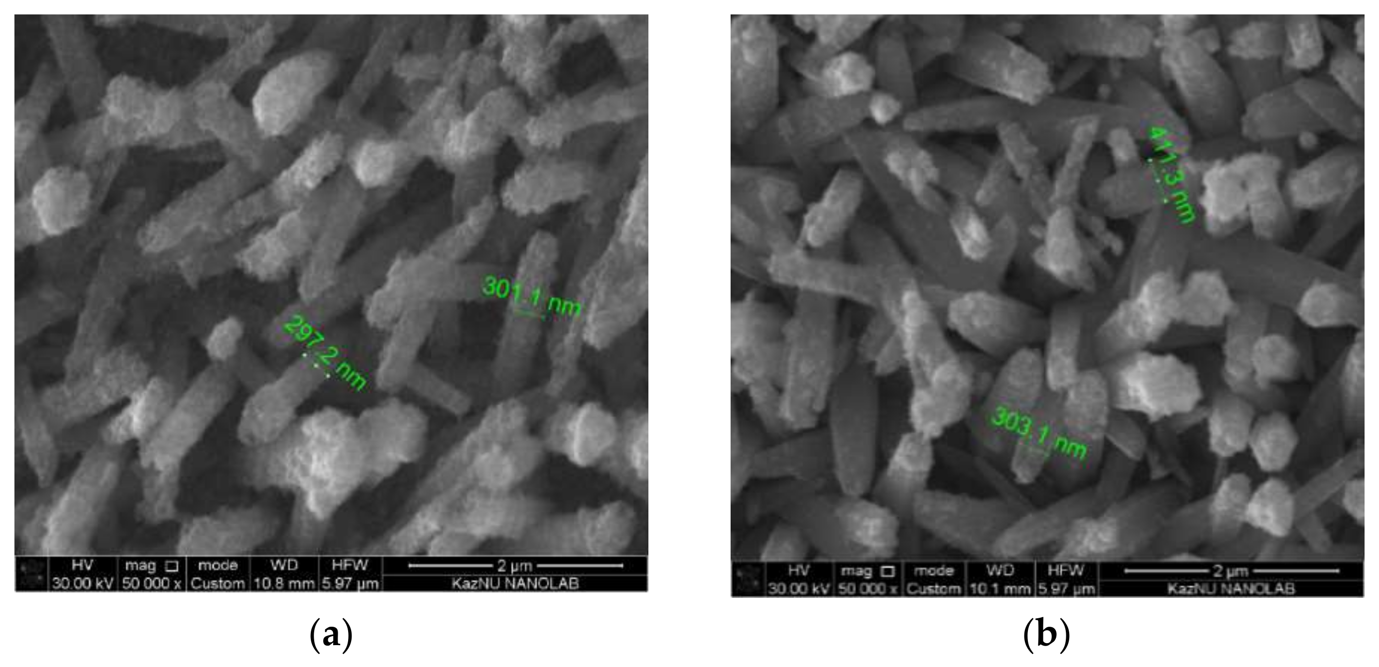
The morphology and elemental composition of obtained samples were investigated using scanning electron microscopes JSM-6490 LA (JEOL) with a tungsten cathode. Analysis of 1D ZnO arrays surface morphology showed the formation of hexagonal rods because of electrochemical synthesis (Figure 1a). The crystal structure of the material obtained was analyzed using an X-ray diffractometer X’pert PRO (PANalitical) with a copper anode of 0.154 nm Cu-Kα. The structural-phase analysis of the deposited layers revealed that the main directions of crystallite growth are (100), (101), and (002), which correspond to the wurtzite phase of (hexagonal) structured ZnO (Figure 1b). However, the peak relating to the direction (002) has a greater intensity, which indicates that the structures are oriented perpendicularly to the substrate.
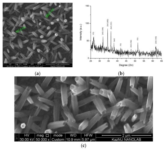
Figure 1.
(a) NRs SEM image, (b) X-ray pattern of arrays obtained, (c) NTs SEM image.
In order to form ZnO nanotubes (NTs), the etching of low-dimensional ZnO NRs should proceed mainly in the direction of the (0001) plane. Selective etching of ZnO NRs to achieve a tubular morphology was confirmed in [14,15,16]. The metastability of ZnO in the (0001) plane leads to the preferential removal of the material in the (0001) plane at speed exceeding the etching rate of the material in other planes, which results in preferential etching in the central part of the NRs. Because ZnO is soluble in an acidic medium, etching of 1D ZnO arrays was conducted through the electrochemical method. Samples with a uniform ZnO array were used as cathodes in an electrochemical cell, the anode of which was a platinum plate, with a 1 V potential supplied and a varied reaction time. Figure 1c shows a typical micrograph of an array of ZnO NTs obtained by selective etching of electrodeposited low-dimensional ZnO rods on a transparent conductive substrate. A homogeneous array of large-area ZnO NRs consisting of 1D structures with well-defined hexagonal cross-sections, the average diameter of which was 200–300 nm, was observed. A detailed study of the micrographic images shows that the etching process begins from the center of the upper surface and advances through the inner part of the rod, which results in the formation of tubes, the sidewalls of which were 10–20 nanometers thick.
For the formation of the composite material ZnO NRs/Ag, matrix of ZnO NRs with surface morphology illustrated in Figure 1a was selected. After deposition of Ag NPs onto the surface of the ZnO NRs, a layer of inclusions formed on the side and end surfaces (Figure 2a,b).
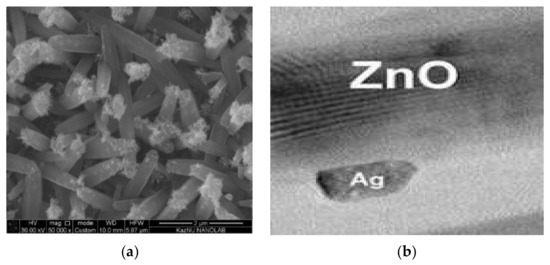
Figure 2.
Surface morphology of 1D ZnO/Ag composite material: (a) SEM; (b) TEM images.
The distribution of Ag NPs was not uniform. In some places, in particular, on the (0001) surface, accumulation of low-dimensional Ag formations was observed, while in others, there was a complete absence (Figure 2a). When studying the 1D ZnO/Ag nanocomposite under transmission microscopy, Ag NPs can be seen to be in good contact with ZnO arrays. The average size of the AgNPs deposited onto the surface of ZnO rods was of the order of 10–20 nm (Figure 2b).
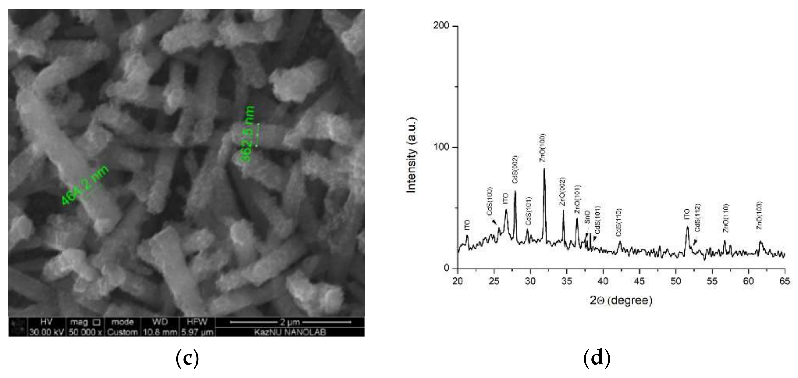
Figure 3a shows the morphology of the NRs array of ZnO/Ag/CdS after 10 cycles of successive ionic layer adsorption and reaction (SILAR) assembly. The deposition of Ag NPs and 10 layers of CdS led to the formation of a heterostructure capping the ZnO rods, creating a relatively thin wrapping layer tens of nanometers in thickness. That the main accumulations of NPs were concentrated on the tops of the ZnO rods can be explained by the large aggregation of plasmonic NPs on the polar plane of the NRs. The average diameter of the 1D composites obtained was around 300 nm. Increasing the number of applications of the narrow-gap CdS semiconductor to 20 led to the formation of a thicker film, increasing the diameter up to approximately 400 nm, which was why the hexagonal structure was not observed in Figure 3b. At 30 cycles of CdS deposition onto the array, the average size of the nanocomposite can exceed 400 nm (Figure 3c). X-ray analysis of the ZnO/Ag/CdS composites showed that the samples were in good accordance with JCPDS 01-077-2306, with peaks indexed at (100), (002), (101), (102), (110), and (112), indicating CdS (Figure 3d).


Figure 3.
(a) SEM image of 10 layers of CdS; (b) SEM image of 20 layers of CdS; (c) SEM image of 30 layers of CdS, and (d) X-ray diffraction analysis.
Assembling CdS layers onto ZnO NTs was conducted in the same manner as onto ZnO NRs. After 10 cycles of layering CdS coating onto a ZnO/Ag composite with tubular morphology (Figure 4a), the inside and outside of which were covered with Ag NPs, a coating forms, in the interior and exterior, similar to that following deposition of CdS onto ZnO/Ag NRs. After increasing the number of cycles up to 20, the deposited material significantly fills the spaces inside the ZnO/Ag NTs, which results in a compaction of the film (Figure 4b).
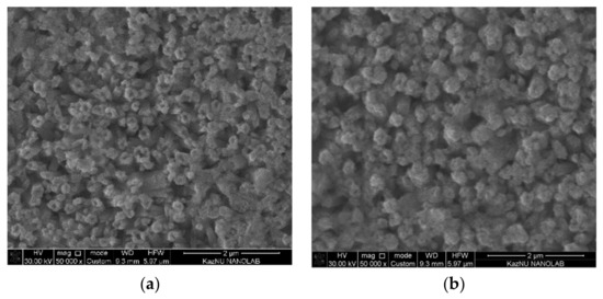
Figure 4.
SEM images of composite materials of ZnO/Ag/CdS tubular forms: (a) 10 layers; (b) 20 layers.
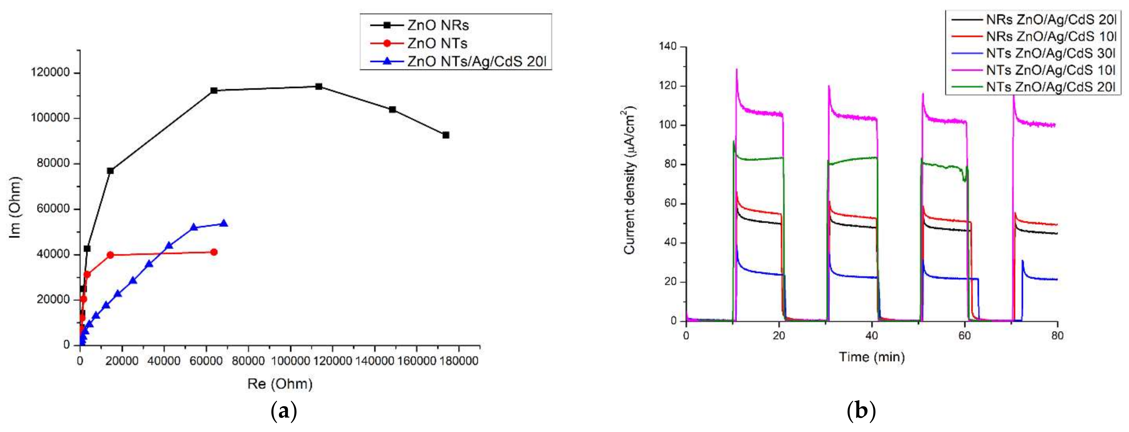
Electron transport in ZnO NRs, ZnO NTs, ZnO NTs/Ag/CdS arrays (Figure 5a) was examined using an impedance meter while immersing the individual photoanodes in an aqueous solution of 0.05 M Na2SO4. The spectra were recorded in darkness at 0.2 V with an amplitude of 5 mA and a frequency range from 500 kHz to 10 MHz. Electrochemical impedance spectroscopy was able to interpret the migration activity of charge carriers and the resistance of interphase charge transfer in the samples. As a rule, a smaller radius in the semicircle of a Nyquist plot implies a lower resistance to electron transfer, indicating faster charging and a higher separation rate of electron-hole pairs [16], which facilitates charge transfer at the solid-liquid interface [17]. The arc radius that corresponds to the impedance of the ZnO NTs (Figure 5a—red curve) was the smallest, indicating a lower electrical resistance in the interface layer, which means increased charge transfer over the semiconductor surface [18]. In this case, the resistance to charge transfer in the NRs (Figure 5a—black curve) was greater in comparison with the NTs and the composites based on them. This means that the use of an array of ZnO NRs as a matrix for the manufacture of a composite material was not relevant. An increase in the resistance of the interfacial charge transfer occurs in arrays of NTs following deposition of Ag and CdS, which was predictable because of the resultant heterostructure (Figure 5a—blue curve). The EIS graphs demonstrate that the unique structure of NTs has a decisive role in significantly improving the performance of PEC.


Figure 5.
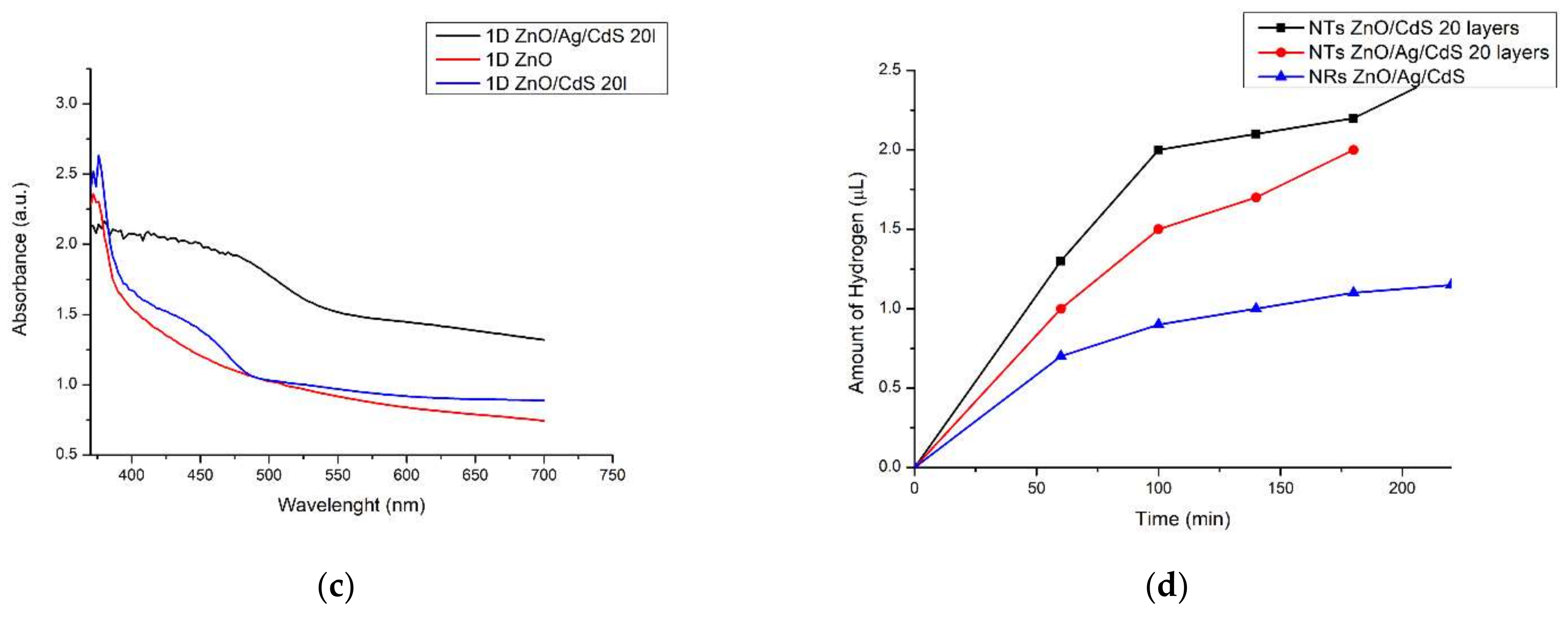
Spectroscopic measurements of structures obtained: (a) impedance spectrum of the photoanodes (ZnO NRs, ZnO NTs and ZnO/Ag/CdS nanocomposite—black, red and blue curves, respectively); (b) JT diagram of photocurrent in nanocomposites; (c) optical absorption spectrum; (d) photocatalytic evolution of hydrogen during the decomposition of water in the PEC cell.
In order to study the photoresponse of the ZnO nanostructure and nanocomposites of ZnO/Ag and ZnO/Ag/CdS, a 60 W xenon lamp and three-electrode electrochemical cell were used. The PEC cell consisted of a fabricated photo-anode, a reference Ag/AgCl electrode, a platinum cathode, and an aqueous solution containing 0.05 M Na2SO4 as an electrolyte. When using Ag NPs deposited between n-type direct-gap semiconductors, more efficient transport of charge carriers occurs. At the same time, such an architecture was more stable under photo-excited transitions and water molecule oxidation since photoinduced excitons rapidly separate, with charge transfer to the phase boundaries. Absorption of the visible fraction of light by the narrow-gap CdS semiconductor caused its excitation, which resulted in the generation of charge carriers. Photogenerated electrons can be quickly extracted and efficiently transferred through the alignment of the type II band in the NTs arrays of nanocomposites, which additionally results in the recovery of water for H2 production. Photoinduced holes that gather in the valence band of CdS contribute to the oxidative reaction of water. Furthermore, plasmonic Ag NPs can generate additional hot electrons and then inject them into the conduction band of the neighboring CdS, which increases the carrier density and speeds up the transfer of photoinduced electrons from CdS to ZnO. Thus, a synergistic effect is observed in the ZnO/Ag/CdS photoanode, which ensures efficient transport and use of photoinduced electrons, ultimately leading to a significant improvement in the characteristics of the PEC processes. The photoinduced current density passing through a cell made of ZnO NTs/Ag/CdS10 layers reaches 50–60 µA/cm2, which is twice the current density when using ZnO NTs/Ag/CdS30 layers (Figure 5b).
Increased current density in the structures of the samples obtained is also explained by an improvement in photon harvesting associated with the expansion of the spectrum to which the active layers are sensitive. This expansion of the spectral sensitivity of the photoanode based on ZnO NTs after depositing CdS NPs to the array is confirmed by the optical absorption spectrum (Figure 5c—blue curve). Two absorption thresholds in ZnO/CdS composites are clearly seen in comparison with the single one in the ZnO nanostructure (Figure 5c—red curve). The first absorption threshold, in the UV region (370 nm), is directly related to ZnO, while the second threshold, in the visible region (470–490 nm), is a manifestation of the optical properties of CdS. The optical absorption spectrum of the ZnO NTs/Ag/CdS heterostructure (Figure 5c—black curve) shows broadening of the spectral sensitivity up to 480 nm, with the absorption threshold in this area related to the Ag NPs.
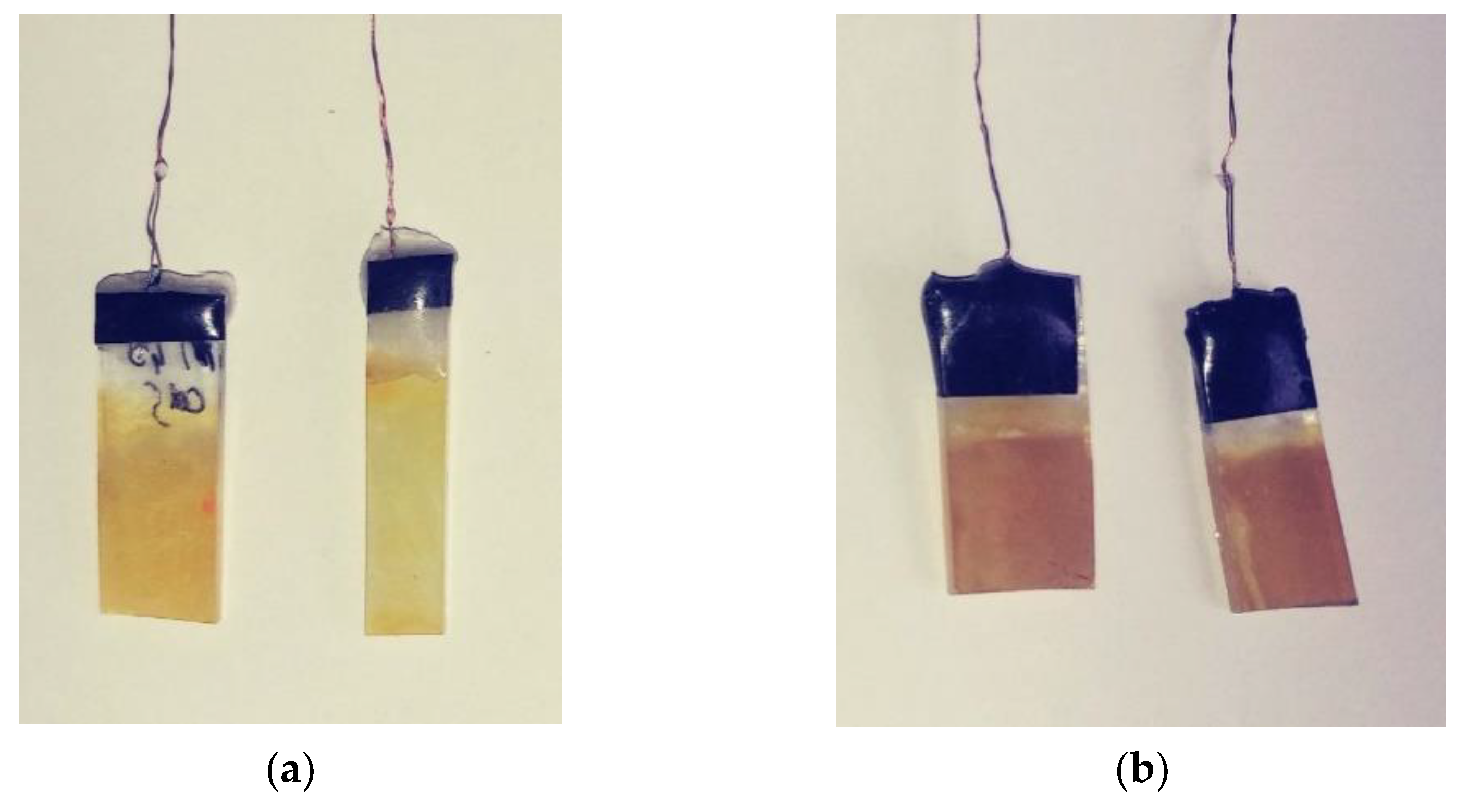
The amount of hydrogen gas, which may have included a portion of oxygen, as gas chromatography was not conducted, released after 200 min of irradiation of the three-component tubular ZnO-based nanocomposite was 2 μL, which was 1.8 times greater than the hydrogen released using a photoanode based on ZnO NRs (Figure 5d). Although photoinduced hydrogen generation using the two-component photoanode ZnO/CdS proceeds twice as fast as the three-component photoanode ZnO/Ag/CdS, the use of the latter has an advantage in photodegradation resistance (Figure 6). As can be seen, the ZnO/Ag/CdS photoanode did not change visually (Figure 6b). At the same time, after a 200 min PEC reaction, the ZnO/CdS photoanode began to pale in color (Figure 6a). At the same time, the degree of degradation of the photoanodes obtained in this work was measured by comparing the electrical conductivity of the working solutions of the PEC cell before and after the photoinduced RedOx reactions. The electrical conductivity of the working solutions was measured by immersing a conductometric S30 electrode in the electrolyte. It is believed that upon dissolution of the photoanode material in the electrolyte, the conductivity of the solution changes due to the appearance of additional ions. A comparison of the electrical conductivity of the working solution before and after the PEC reactions with ZnO/Ag/CdS photoanode showed an insignificant increase from 177.5 µS/cm to 179 µS/cm, which indicates a low degradation of the photoanode during a 200-min cycle. The test of conductivity of the working solution of PEC reaction with ZnO/CdS photoanode showed a dramatic increase of conductivity from 178 µS/cm to 240 µS/cm. This can indirect evidence of the dissolution of the ZnO/CdS photoanode.
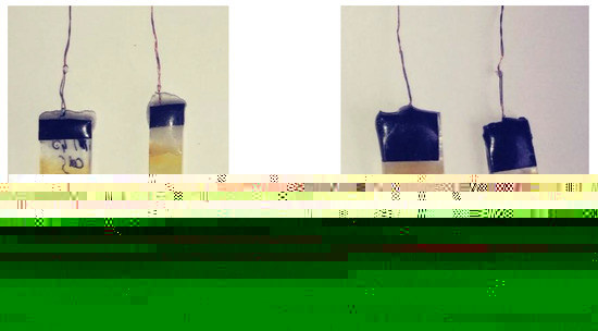
Figure 6.
Photographic image of the anodes made before and after the PEC reaction: (a) 1D ZnO/CdS; (b) 1D ZnO/Ag/CdS.
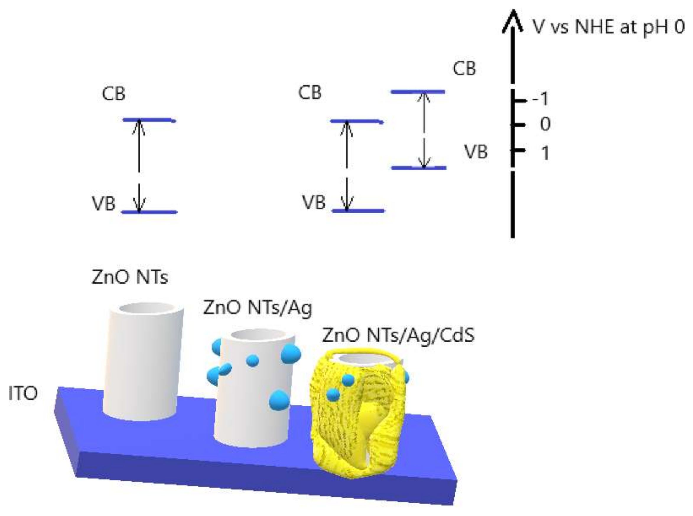
The improvement of stability can be explained graphically. Figure 7 is a diagram showing the levels of the valence band (VB) and conduction band (CB) relative to a normal hydrogen electrode (NHE). As can be seen from the figure, CB of the ZnO NTs and CdS above the zero level, which is sufficient for hydrogen reduction. In this case, the diagram shows that the level of the CB of CdS was more negative than CB of ZnO, which improves the transport of charges in the material, and, therefore, improves the photocatalytic properties. Ag NPs interspersed between the layers of ZnO and CdS serve as an additional charge transfer bridge.

Figure 7.
Schematic representation of obtained photoactive materials with respect to NHE at pH 0.
Finite-Difference Time-Domain Simulation (FDTD)
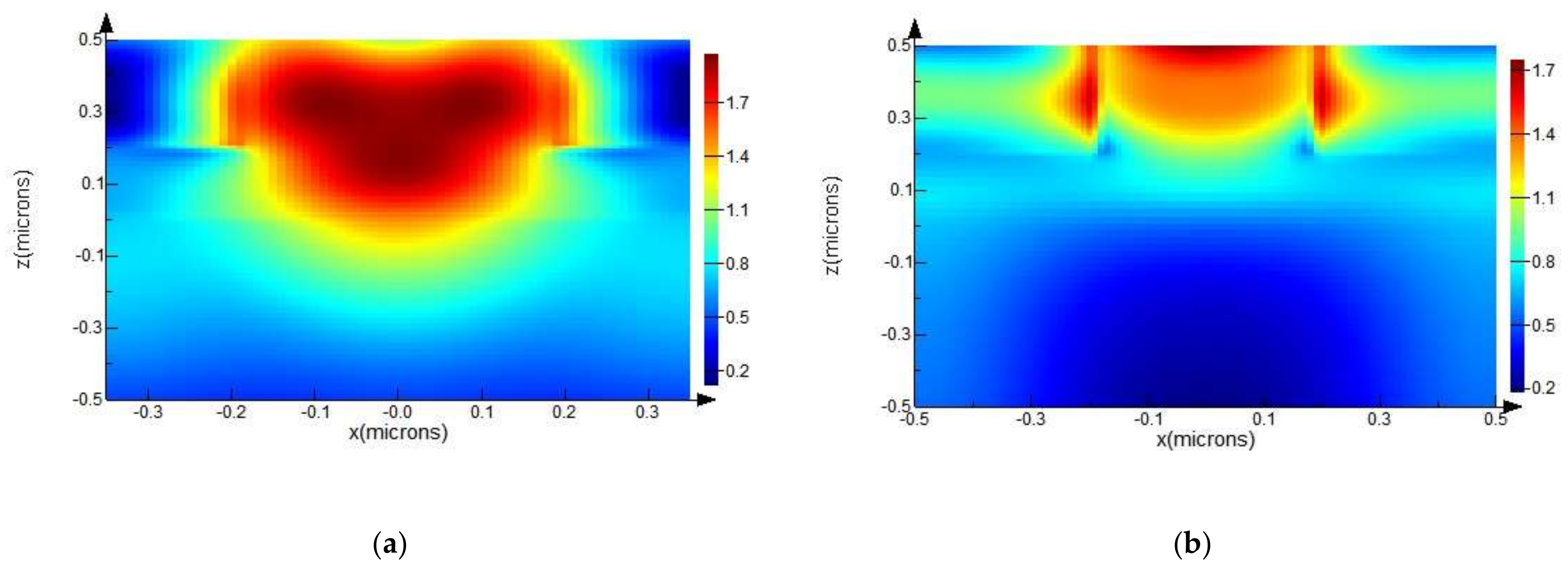
FDTD simulations (Lumerical FDTD Solutions 8.19.1584) were employed in order to solve Maxwell’s equations and obtain theoretical values for several parameters such as electric field as a function of wavelength. The sample was represented as a periodic array of cylindrical structures. The advantage of symmetry was taken to optimize simulation times. The range of interest was set to be between 0.4 and 0.7 um.
From the graphical representations given in Figure 8a,b, we can clearly see that field lines are more intense, apparent from relative numerical values on the scale bar, and the area of higher intensity is much broader in the case of ZnO NRs with Ag NPs.
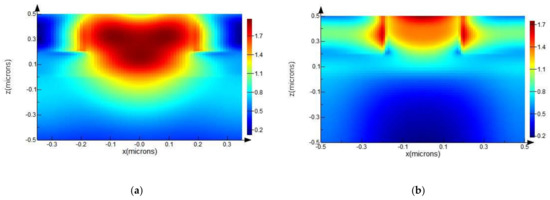
Figure 8.
Spatial distribution of electric field intensity at 700 nm wavelength, calculated from an FDTD simulation, for ZnO NRs with radii of 200 nm (a) with Ag NPs with radii of 20 nm; and (b) without Ag NPs.
3. Materials and Methods
During experimental work, pure commercial reagents were used.
Synthesis of nanoscale arrays of 1D structures of ZnO was performed using electrochemical methods. The technique consists of the formation of thin coatings on the surface of a transparent conductive substrate (ITO glass) in order to perform the function of the working electrode of the three-electrode cell. Ag/AgCl and platinum foil were utilized as the reference and countercurrent electrodes, respectively. The capacity of the electrochemical cell was 50 mL. Before carrying out experimental work, the ITO glass with a resistance of 8 Ω/cm2 was thoroughly cleaned.
3.1. Synthesis of ZnO NRs and ZnO NTs
ZnO NRs were synthesized via the applied constant negative potential of 0.9 ± 0.05 V in an aqueous solution, with 0.005 M Zinc nitrate and 0.5 M KCl. Electrodeposition of ZnO NRs was carried out in a temperature range from 50 to 80 °C for 20 min. The formation of ZnO NTs was conducted by selective etching of ZnO NRs. The process of selective etching proceeded in a potentiostatic mode in a three-electrode cell. The electrolyte of the system was a solution containing 0.05 M Zn(NO3)2*6H2O and 0.5 M KCl. The temperature was 70 °C time 120 min, and applied positive voltage was 1 V. After synthesis, the samples were washed in distilled water and annealed in a muffle furnace at a temperature of 500 °C, over a time of 2 h.
3.2. Synthesis of ZnO/Ag Nanocomposites
Ag NPs were deposited on the surface of ZnO NRs and ZnO NTs in two steps. Firstly, the formation of Ag NPs was carried out utilizing the hydrothermal method from an aqueous solution of 0.001 M silver nitrate and 0.038 M sodium citrate, at a temperature of 97–100 °C for 2 min. As a result of mixing the reagents, the solution took on a yellow color. Then, the heated solution was placed in a thermostatically controlled oil cooler, the temperature of which was maintained around −5 °C. The synthesis took more than 5 min, after which the solution became cloudy due to the agglomeration of Ag NPs. Secondly, the ZnO/Ag composite was obtained using electrodeposition of Ag NPs on ZnO arrays [14] through the application of a negative voltage of 1 ± 0.1 V for 90 s. Finally, the samples were washed in deionized water.
3.3. Forming ZnO/Ag/CdS Core/Shell Structure
The deposition of CdS layers proceeded in accordance with the SILAR adsorption technique described in [10,15]. Glass coated with the ZnO matrix was dipped into the first beaker containing Cd2 + (5 mM Cd (NO3)2) cations, which were adsorped during a dip time of 10 s. After that, the samples were immersed in deionized water in the second beaker for 20 s, which was necessary to remove excess ions weakly bound to the ZnO arrays. The formation of CdS was achieved by immersing the sample into a beaker of S2− (5 mM Na2S) anions for 10 s. After that, the samples were subjected again to washing in deionized water in another beaker for 20 s. The thickness of the CdS coating deposited onto the ZnO matrix was controlled by the number of immersion cycles.
When performing SILAR, the following parameters were followed: (1) the rate of immersion of the substrate into the solution was 50 mm/min; (2) the rate of removal of the substrate from the solution was 10 mm/min; and (3) the time between vessels with different solutions was 10 s.
4. Conclusions
Composite photocatalytic materials ZnO/Ag/CdS were formed by three-step synthesis, and their morphology and optical and photocatalytic properties were studied. Optimal geometric dimensions of the CdS layers on 1D ZnO structures using electrochemical deposition and SILAR methods were determined. Following the addition of Ag NPs to the ZnO/CdS nanocomposite, photo corrosion damage of the active photoanode layers during water decomposition decreased. Along with improved corrosion properties, an increase in hydrogen evolution was observed. The enhancement of properties upon the addition of Ag NPs was supported by simulation analysis as well.
Author Contributions
Conceptualization, B.S.; Methodology, B.S.; Software, N.A.; Validation, N.B., D.B.; Formal analysis, N.B.; Investigation, S.K.; Data curation, N.A.; Writing—original draft preparation, D.B.; Writing—review and editing, B.S.; Visualization, S.K.; Supervision, N.B.; Project administration, B.S.; Funding acquisition, N.B. All authors have read and agreed to the published version of the manuscript.
Funding
This research was funded by Ministry of Science and Education of the Republic of Kazakhstan, grant number AP08052381.
Conflicts of Interest
The authors declare no conflict of interest. The funders had no role in the design of the study; in the collection, analyses, or interpretation of data; in the writing of the manuscript, or in the decision to publish the results.
References
- Sathre, R.; Scown, C.D.; Morrow, W.R.; Stevens, J.C.; Sharp, I.D.; Ager, J.W.; Walczak, K.; Houle, F.A.; Greenblatt, J.B. Life-cycle net energy assessment of large-scale hydrogen production via photoelectrochemical water splitting. Energy Environ. Sci. 2014, 7, 3264–3278. [Google Scholar] [CrossRef]
- Wang, G.M.; Ling, Y.C.; Wang, H.Y.; Lu, X.H.; Li, Y. Chemically modified nanostructures for photoelectrochemical water splitting. J. Photochem. Photobiol. C-Photochem. Rev. 2014, 19, 35–51. [Google Scholar] [CrossRef]
- Li, Y.; Zhang, J.Z. Hydrogen generation from photoelectrochemical water splitting based on nanomaterials. Laser Photonics Rev. 2010, 4, 517–528. [Google Scholar] [CrossRef]
- Qi, H.; Alexson, D.; Glembocki, O.; Prokes, S.M. Plasmonic coupling on dielectric nanowire core-metal sheath composites. Nanotechnology 2010, 21, 085705. [Google Scholar] [CrossRef] [PubMed]
- Xiang, Q.J.; Yu, J.G.; Cheng, B.; Ong, H.C. Microwave-Hydrothermal Preparation and Visible-Light Photoactivity of Plasmonic Photocatalyst Ag-TiO2 Nanocomposite Hollow Spheres. Chem.-Asian J. 2010, 5, 1466–1474. [Google Scholar] [CrossRef] [PubMed]
- Qi, H.; Alexson, D.; Glembocki, O.; Prokes, S.M. The effect of size and size distribution on the oxidation kinetics and plasmonics of nanoscale Ag particles. Nanotechnology 2010, 21, 215706. [Google Scholar] [CrossRef] [PubMed]
- You, J.B.; Zhang, X.W.; Fan, Y.M.; Yin, Z.G.; Cai, P.F.; Chen, N.F. Effects of the morphology of ZnO/Ag interface on the surface-plasmon-enhanced emission of ZnO films. J. Phys. D-Appl. Phys. 2008, 41, 205101. [Google Scholar] [CrossRef]
- Osterloh, F.E. Inorganic nanostructures for photoelectrochemical and photocatalytic water splitting. Chem. Soc. Rev. 2013, 42, 2294–2320. [Google Scholar] [CrossRef] [PubMed]
- Walter, M.G.; Warren, E.L.; Mckone, J.R.; Boettcher, S.W.; Mi, Q.X.; Santori, E.A.; Lewis, N.S. Solar Water Splitting Cell. Chem. Rev. 2011, 111, 5815. [Google Scholar] [CrossRef]
- Tak, Y.; Hong, S.J.; Lee, J.S.; Yong, K. Fabrication of ZnO/CdS core/shell nanowire arrays for efficient solar energy conversion. J. Mater. Chem. 2009, 19, 5945–5951. [Google Scholar] [CrossRef] [Green Version]
- Abdullin, K.A.; Bakranov, N.B.; Ismailov, D.V.; Kalkozova, J.K.; Kumekov, S.E.; Podrezova, L.V.; Cicero, G. Composite materials based on nanostructured zinc oxide. Semiconductors 2014, 48, 471–475. [Google Scholar] [CrossRef]
- An, C.H.; Peng, S.N.; Sun, Y.G. Facile Synthesis of Sunlight-Driven AgCl:Ag Plasmonic Nanophotocatalyst. Adv. Mater. 2010, 22, 2570–2574. [Google Scholar] [CrossRef] [PubMed]
- Maier, S.A.; Brongersma, M.L.; Kik, P.G.; Meltzer, S.; Requicha, A.A.G.; Atwater, H.A. Plasmonics—A route to nanoscale optical devices. Adv. Mater. 2001, 13, 1501–1505. [Google Scholar] [CrossRef]
- Brolo, A.G. Plasmonics for future biosensors. Nat. Photonics 2012, 6, 709–713. [Google Scholar] [CrossRef]
- Bakranov, N.; Kudaibergenov, S. Layer-by-Layer Thin Films and Coatings Containing Metal Nanoparticles in Catalysis. Metal Nanoparticles Catal. 2017. [Google Scholar] [CrossRef] [Green Version]
- Wei, R.B.; Kuang, P.Y.; Cheng, H.; Chen, Y.B.; Long, J.Y.; Zhang, M.Y.; Liu, Z.Q. Plasmon-Enhanced Photoelectrochemical Water Splitting on Gold Nanoparticle Decorated ZnO/CdS Nanotube Arrays. ACS Sustain. Chem. Eng. 2017, 5, 4249–4257. [Google Scholar] [CrossRef]
- Han, W.J.; Ren, L.; Qi, X.; Liu, Y.D.; Wei, X.L.; Huang, Z.Y.; Zhong, J.X. Synthesis of CdS/ZnO/graphene composite with high-efficiency photoelectrochemical activities under solar radiation. Appl. Surf. Sci. 2014, 299, 12–18. [Google Scholar] [CrossRef]
- Ren, C.L.; Yang, B.F.; Wu, M.; Xu, J.A.; Fu, Z.P.; Lv, Y.; Guo, T.; Zhao, Y.X.; Zhu, C.Q. Synthesis of Ag/ZnO nanorods array with enhanced photocatalytic performance. J. Hazard. Mater. 2010, 182, 123–129. [Google Scholar] [CrossRef] [PubMed]


Publisher’s Note: MDPI stays neutral with regard to jurisdictional claims in published maps and institutional affiliations. |
© 2021 by the authors. Licensee MDPI, Basel, Switzerland. This article is an open access article distributed under the terms and conditions of the Creative Commons Attribution (CC BY) license (https://creativecommons.org/licenses/by/4.0/).