Article

High-Speed GaN-Based Superluminescent Diode for 4.57 Gbps Visible Light Communication

1
Key Laboratory for Information Science of Electromagnetic Waves (MoE), School of Information Science and Technology, Fudan University, Shanghai 200438, China
2
Shanghai Engineering Research Center of Low-Earth-Orbit Satellite Communication and Applications, Shanghai 200438, China
3
Shanghai Collaborative Innovation Center of Low-Earth-Orbit Satellite Communication Technology, Shanghai 200438, China
4
Peng Cheng Laboratory, Shenzhen 518038, China
5
China Mobile Research Institute, Beijing 100053, China
*
Author to whom correspondence should be addressed.
Crystals 2022, 12(2), 191; https://doi.org/10.3390/cryst12020191
Submission received: 16 December 2021 / Revised: 21 January 2022 / Accepted: 24 January 2022 / Published: 27 January 2022
(This article belongs to the Special Issue Advances in GaN-Based Optoelectronic Materials and Devices)

Abstract

:
Visible light communication (VLC) is a promising technology for next-generation high-speed optical wireless data links. Among various transmitters, GaN-based superluminescent diodes (SLDs) show interesting characteristics, including a large modulation bandwidth, droop free and low speckle noise, which makes them attractive for VLC applications. In this work, we design and fabricate a blue-emitting SLD utilizing tilted facet configuration. Using SLD as the light source, a VLC system is experimentally demonstrated. A record data rate of 4.57 gigabit per second (Gbps) is achieved with adaptive bit-loading discrete multiple tone (DMT) modulation, while the highest modulation format reaches 256 quadrature amplitude modulation (QAM). The corresponding bit error rate (BER) is ~3.5 × 10⁻³, which is below the forward error correction (FEC) threshold of 3.8 × 10⁻³.

1. Introduction

In recent years, the rapid growth of wireless data demands has called for a large data rate and low latency data links. Beyond conventional RF-based technologies, various emerging technologies have been studied, and visible light communication (VLC) is one of them. VLC, or LiFi technology, has drawn much attention, owing to its high security, durability against electromagnetic interference (EMI), use of an unlicensed spectrum, and combination of illumination and communication [1,2,3].
InGaN-based light-emitting diodes (LEDs) have been widely used as the transmitter of VLC systems, due to their wide availability, long lifespan, and low cost. However, the modulation bandwidth of a typical LED is limited to tens or hundreds of MHz, owing to the spontaneous emission nature. Hence, the transmission data rate of LED-based VLC systems might be limited. On the other hand, laser diodes (LDs) have a much higher bandwidth of several GHz and a high data rate of several Gbps, but the speckle noise, as well as the potential safety concerns, limit the mass deployment of LD-based VLC systems [4].
Superluminescent diodes (SLDs) have the advantages of both LEDs and LDs, and have lately been studied as the transmitter in VLC systems with high-speed, droop-free and low speckle noise characteristics [5,6]. In this work, a blue SLD was fabricated using a tilted facet configuration with a tilting angle of 8.3° on the front facet. We experimentally demonstrate a VLC system based on this blue SLD, which has reached a record data rate of up to 4.57 Gbps.

2. Materials and Methods

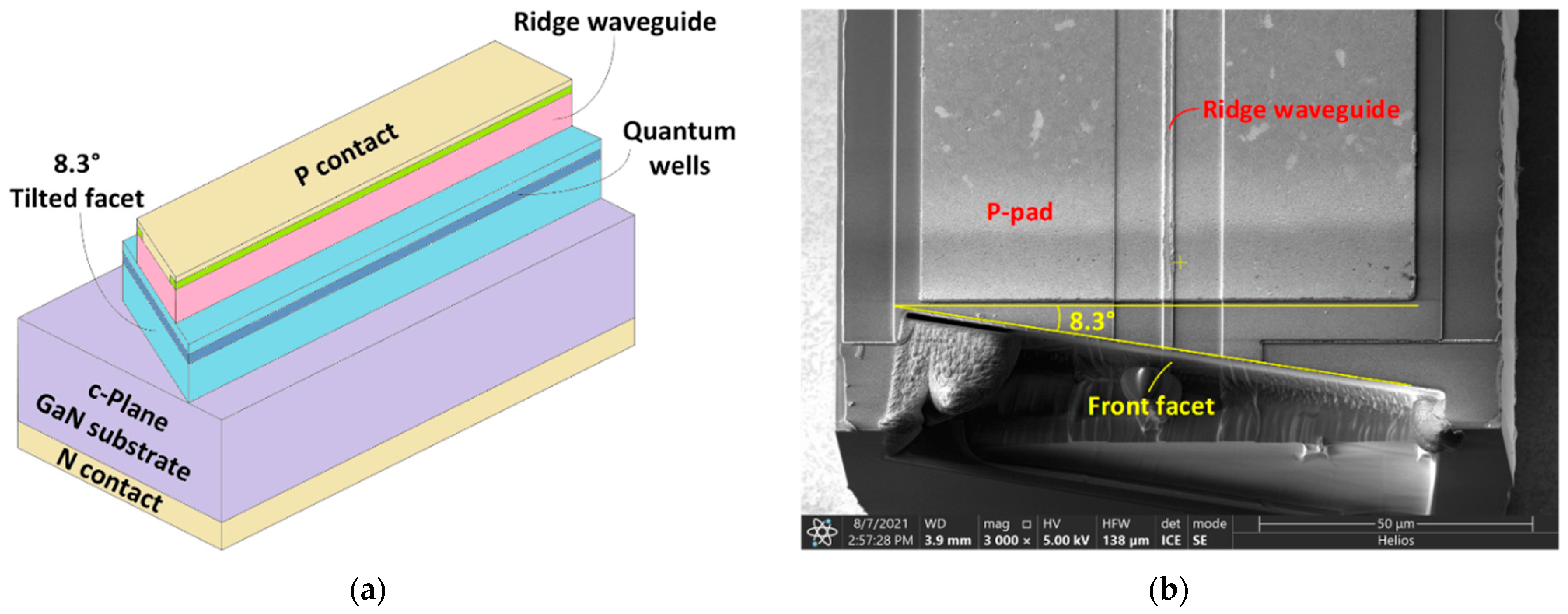
2.1. Blue SLD Structure

The epitaxial structure of the device is grown on a c-plane GaN substrate using a metal–organic chemical vapor deposition (MOCVD) technique. The SLD is fabricated based on a conventional laser epi-structure [7], consisting of In0.15Ga0.85N/GaN quantum wells as the active region, together with AlGaN cladding layers, GaN waveguiding layers and an AlGaN electron blocking layer. The top GaN layer is highly Mg-doped in order to guarantee high-quality ohmic contact. The SLD has an etched ridge waveguide structure and an 8.3° tilted facet, as illustrated in Figure 1a. This angle is controlled for minimizing the direct reflectance from the front facet, and thus the formation of a resonant cavity is suppressed. In particular, anti-reflective (AR) coating is not needed for this structure. The device mesa and 2 μm ridge waveguide is defined by UV photolithography and plasma etching. The Pt/Au and Ti/Al/Ti/Au metal contacts are deposited using RF sputtering as p- and n-contacts [7]. The tilted facet is defined using focus ion beam (FIB) milling technology using FEI Helios System. In order to increase the output optical power, the back facet of the SLD is coated with a highly reflective (HR) mirror with reflectivity over 90%. The top view of the fabricated device is shown in Figure 1b.

2.2. The Principle of Adaptive Bit-Loading Discrete Multiple Tone (DMT) Modulation Scheme

On–off keying (OOK) is widely used as a modulation scheme for data transmission experiments, but due to the low spectral efficiency (SE), the data rate is limited. In this work, we use the adaptive discrete multiple tone (DMT) scheme for optical wireless communication and achieve a data rate much higher than those using OOK modulation.
In the bit-loading DMT modulation scheme, the utilized frequency spectrum is uniformly divided into multiple communication channels with carriers totally separated. The carriers for those separated communication channels are called subcarriers. There is no interference across subcarriers. In the VLC systems, only amplitude modulation is considered. These systems are called intensity modulation direct detection (IM-DD) systems. A structure of Hermitian symmetry is utilized in the DMT modulation scheme to obtain a real-valued signal through inverse discrete Fourier transform (IDFT), then the requirement of IM-DD systems is satisfied [8,9].
To better assess the characteristic of the channel for VLC links, a training process is included in the adaptive bit-loading DMT scheme. A 4-QAM training signal is transmitted and then the error vector magnitude (EVM) is calculated, so that the subcarrier signal-to-noise ratio (SNR) can be estimated properly. According to the estimated SNR of the VLC channel, the LC algorithm introduced in [10] is utilized to complete bit loading for each subcarrier. The SE is maximized in this way, which can even approach the Shannon limit. After training, the communication signal is transmitted and then collected at the receiver end (Rx). Further digital signal processing (DSP) is carried out. The received signal is demodulated with posteriori knowledge of the VLC channel, and then the bit error rate (BER) is calculated.

2.3. Experimental Setup

The light output current–voltage (L-I-V) measurement was carried out in a device tester with a thermal-electric cooled SLD mount, a Keithley 2400 source measure unit (SMU), and an integrating sphere with a calibrated Si photodetector (Labsphere LPMS-020-SF-SDTP, North Sutton, NH, USA). The optical spectra were collected using a spectrometer (Ocean Optics QE Pro, Orlando, FL, USA). All measurements were performed at room temperature.
The schematic and experimental setup of the SLD-based VLC system using the bit-loading DMT modulation scheme is depicted in Figure 2. For proof-of-concept demonstration, the signal modulation and demodulation processes were performed offline using MATLAB. Firstly, a pseudo-random binary sequence was generated. We used the adaptive bit-loading DMT modulation scheme containing 256 subcarriers, the QAM order of which depended on SNR estimation. The up-sampling factor was 2. The signal was loaded into an arbitrary waveform generator (AWG, Keysight M8190A, Santa Clara, CA, USA) with a maximal sample rate of 12 GSa/s. Afterwards, the signal was amplified by an electronic amplifier (iXblue Photonics DR-AN-10-MO, Lannion, France), and attenuated by an attenuator (Key-Press Attenuator kT2.5-30/1S-2S, Shenzhen, China). The 290 mA DC bias generated by a source measure unit (Keithley 2400, Santa Clara, CA, USA) was coupled with the modulated signal by the bias-tee (Mini-Circuits ZFBT-4R2GW-FT+, Brooklyn, NY, USA). A thermoelectric cooler (TEC) was attached to the SLD so as to keep the device at a constant temperature. The transmission distance was set as ~1 m as a test bed for practical deployment of the VLC system. An iris was placed in front of the Rx to reduce the spontaneous emission component of the beam. Finally, the light was received by a customized Si avalanche photodetector (APD) with a bandwidth exceeding 1 GHz. Then the optical signal was converted into an electrical signal and was resampled by the oscilloscope (OSC, Keysight DSO9404A, Santa Rosa, CA, USA) for offline signal processing. The maximal sample rate of the OSC was 20 GSa/s. The frequency response of the SLD-based VLC system was tested by a network analyzer (Agilent Technologies PNA-L N5230C, Santa Clara, CA, USA).

3. Results

The optical and electrical characteristics of the SLD are reported in Section 3.1, and the results of the communication experiment are outlined in Section 3.2 below.

3.1. Device Characterizations

Figure 3 presents the optical power vs. current and voltage vs. current curves of the fabricated SLD tested at room temperature. The device has a turn-on voltage of ~3.1 V, which is similar to a typical GaN-based LED. With increasing injection current exceeding 80 mA, a super-linear L-I curve is observed, suggesting that the device entered the amplified spontaneous emission regime, which is typical for an SLD. The optical power increases to ~4.46 mW under the injection current of 290 mA.
In Figure 4a, we plot the emission spectra of the SLD under different injection currents. A blue shift of the emission peak is observed with increasing injection current. The emission peak changes from ~447 nm at 40 mA to ~441 nm at 200 mA. This is mainly attributable to the band filling effect [11]. Figure 4b shows the change in the emission peak position and the full-width at half maximum (FWHM) against the injection current. A fast decrease in peak FWHM, from ~19 nm at 40 mA to ~10 nm at 80 mA, can be observed, suggesting the onset of the superluminescence effect. This matches the L-I characteristics shown in Figure 3 well. The SLD has a relatively broad spectrum, with FWHM of ~12 nm at a high injection current of 300 mA.

3.2. Data Communication Performance

We firstly use a network analyzer to observe the frequency response of the SLD-based VLC system, and the result is shown in Figure 5. When the injection current exceeds 80 mA, there is a significant increase in modulation, suggesting that the SLD operating in the amplified spontaneous emission regime has a better frequency response characteristic. The device shows a −10 dB and −20 dB bandwidth beyond 700 MHz and 1.3 GHz, respectively.
In the data communication experiment where SLD is used as the transmitter, the driving current and the amplitude of the signal should be optimized for communication applications. Thus, we perform a series of measurements to find the optimal working condition of the SLD transmitter for achieving a high data rate. We test the average QAM order under a bias current from 180 mA to 320 mA, with a step of 10 mA, and under the peak-to-peak voltage (Vpp) generated by the AWG, from 350 mV to 650 mV, with a step of 50 mV. As shown in Figure 6, to attain the highest QAM order, the Vpp is set at 500 mV, and the driving current of 290 mA is set for the DC bias of the SLD. According to the device characterization results, the corresponding operating voltage is ~6.98 V, the emission peak is ~442 nm, and the FWHM is ~12 nm at 290 mA. The −3 dB and −20 dB bandwidth of the VLC system are 110 MHz and 1.4 GHz, respectively.
The gain control voltage of the amplifier is set as 1 V, and an attenuation of 5 dB is set by the attenuator. To reduce the spontaneous emission component of the beam, an iris is placed in front of the Rx. The utilized bandwidth is adjusted to achieve a higher data rate in the experimental system. We test the transmission rate using a modulation bandwidth from 1 GHz to 1.425 GHz, with a step of 250 MHz. When testing the data rate, the BER is strictly controlled under the forward error correction (FEC) threshold 3.8 × 10⁻³. As is shown in Figure 7a, the optimized bandwidth is tested as 1.35 GHz. The SNR and allocated bits for each subcarrier are demonstrated in Figure 7b. The constellation diagrams for different QAM orders in this experiment are also included. From the constellation diagrams, we can observe a clear separation of constellation points, which indicates a relatively good SNR. In the SLD-based VLC data link, the highest QAM order reaches six. At a data rate of 4.57 Gbps, the BER is ~3.5 × 10⁻³, which satisfied the forward error correction (FEC) standard of 3.8 × 10⁻³.

4. Discussion

Table 1 summarizes the device performance of recently reported GaN-based SLDs for high-speed modulation applications. The emission wavelength, spectral FWHM, modulation bandwidth, achieved data rate and modulation scheme are compared. In 2016, a group of researchers from KAUST utilized a 405 nm SLD as a transmitter to transmit data at 1.3 Gbps using an OOK modulation scheme [12]. In 2018, the same group reported a blue SLD-based VLC link that enabled a data rate of 1.45 Gbps using an NRZ-OOK modulation scheme [5]. In 2019, KAUST and Fudan University utilized a 443 nm c-GaN SLD with a bit-loading DMT modulation scheme, and reached a data rate of 3.4 Gbps [8]. In 2020, a 443 nm SLD on a c-GaN substrate was demonstrated with a 750 MHz modulation bandwidth. A data rate of 3.8 Gbps was reported [13]. The University of New Mexico successfully fabricated an m-GaN SLD and reached a modulation bandwidth of 2.5 GHz [14]. A c-GaN SLD-based VLC system with an MAPNN-CAP modulation scheme was reported in 2020, which contained neural network applications [15]. In this work, we reported a high-speed VLC system with a data rate of 4.57 Gbps, utilizing a 442 nm SLD as a transmitter, partially attributed to the optimized design and fabrication of the SLD device, and the high spectral efficiency of the bit-loading modulation scheme. The record data transmission rate achieved may be attributed to the high-performance blue SLD and the optimized adaptive DMT modulation scheme used for higher spectral efficiency, which approaches the Shannon limit. Compared with other SLDs, the demonstrated SLD shows a large modulation bandwidth, as well as a good frequency response in the range of 0–1.35 GHz. The narrow (~2 μm) ridge waveguide structure might be one of the main factors enabling high-frequency performance in the compact SLD emitter. A device with a small form factor enjoys a reduced RC time constant, making it promising for high-speed operations.

5. Conclusions

In this work, a 442 nm SLD is fabricated with a 8.3° tilted angle on its front facet. A high-speed blue SLD-based VLC system is demonstrated with a record transmission rate of 4.57 Gbps and a BER of 3.5 × 10⁻³, which is below the FEC BER limit of 3.8 × 10⁻³. The modulation bandwidth is 1.35 GHz. Adaptive bit-loading DMT is an efficient modulation scheme. Our work suggests that GaN-based SLD is a promising transmitter to build high data rate, high-speed VLC systems, benefiting from the large modulation bandwidth, with the possibility of enabling other functionalities, including simultaneous lighting and sensing.

Author Contributions

Device testing, data analysis and writing the manuscript: D.L.; modulation algorithm: F.H.; device fabrication: J.W., C.M. and S.W.; VLC testing: Y.H., J.H., S.Y. and Y.M.; writing-review and editing: J.S., J.Z., Z.L. and L.X.; supervision and review: N.C. and C.S. All authors have read and agreed to the published version of the manuscript.

Funding

This research is partially funded by the Natural Science Foundation of China Project, grant number 61925104, 62031011; Natural Science Foundation of Shanghai, grant number 21ZR1406200; Peng Cheng Laboratory project, grant number PCL2021A14; Fudan University-CIOMP Joint Fund; The joint project of China Mobile Research Institute & X-NET.

Institutional Review Board Statement

Not applicable.

Informed Consent Statement

Not applicable.

Data Availability Statement

Data is available upon request.

Acknowledgments

The authors thank Luonan Sun from Jiangsu Institute of Advanced Semiconductors and the characterization &test facilities at Suzhou Institute of Nano-Tech and Nano-Bionics (SINANO), CAS for the assistance in FIB milling.

Conflicts of Interest

The authors declare no conflict of interest. The funders had no role in the design of the study; in the collection, analyses, or interpretation of data; in the writing of the manuscript, or in the decision to publish the results.

References

  1. Chi, N.; Zhou, Y.; Wei, Y.; Hu, F. Visible Light Communication in 6G: Advances, Challenges, and Prospects. IEEE Veh. Technol. Mag. 2020, 15, 93–102. [Google Scholar] [CrossRef]
  2. Shen, C.; Ma, C.; Li, D.; Hu, J.; Li, G.; Zou, P.; Zhang, J.; Li, Z.; Chi, N. High-speed visible laser light communication: Devices, systems and applications. In Proceedings of the Broadband Access Communication Technologies XV, San Diego, CA, USA, 6–12 March 2021; SPIE: San Diego, CA, USA, 2021; Volume 11711, p. 1171109. [Google Scholar]
  3. Guo, Y.; Alkhazragi, O.; Kang, C.H.; Shen, C.; Mao, Y.; Sun, X.; Ng, T.K.; Ooi, B.S. A tutorial on laser-based lighting and visible light communications: Device and technology. Chin. Opt. Lett. 2019, 17, 040601. [Google Scholar] [CrossRef]
  4. Monavarian, M.; Rashidi, A.; Feezell, D. A Decade of Nonpolar and Semipolar III-Nitrides: A Review of Successes and Chal-lenges. Phys. Status Solidi (A) 2019, 216, 1800628. [Google Scholar]
  5. Alatawi, A.A.; Holguin-Lerma, J.A.; Kang, C.H.; Shen, C.; Subedi, R.C.; Albadri, A.M.; Alyamani, A.Y.; Ng, T.K.; Ooi, B.S. High-power blue superluminescent diode for high CRI lighting and high-speed visible light communication. Opt. Express 2018, 26, 26355–26364. [Google Scholar] [CrossRef] [Green Version]
  6. Shen, C.; Ng, T.K.; Leonard, J.T.; Pourhashemi, A.; Nakamura, S.; Denbaars, S.; Speck, J.S.; Alyamani, A.Y.; El-Desouki, M.M.; Ooi, B.S. High-brightness semipolar (2021) blue InGaN/GaN superluminescent diodes for droop-free solid-state lighting and visible-light communications. Opt. Lett. 2016, 41, 2608–2611. [Google Scholar] [CrossRef]
  7. Rumbolz, C.; Brüderl, G.; Leber, A.; Eichler, C.; Furitsch, M.; Avramescu, A.; Miler, A.; Lell, A.; Strauß, U.; Härle, V. Development of AlInGaN based blue-violet lasers on GaN and SiC substrates. Phys. Status Solidi 2006, 203, 1792–1796. [Google Scholar] [CrossRef]
  8. Hu, F.; Li, G.; Zou, P.; Hu, J.; Chen, S.; Liu, Q.; Zhang, J.; Jiang, F.; Wang, S.; Chi, N. 20.09-Gbit/s Underwater WDM-VLC Transmission based on a Single Si/GaAs-Substrate Multichromatic LED Array Chip. In Proceedings of the 2020 Optical Fiber Communications Conference and Exhibition (OFC), San Diego, CA, USA, 8–12 March 2020; pp. 1–3. [Google Scholar]
  9. Shen, C.; Holguin-Lerma, J.A.; Alatawi, A.A.; Zou, P.; Chi, N.; Ng, T.K.; Ooi, B.S. Group-III-Nitride Superluminescent Diodes for Solid-State Lighting and High-Speed Visible Light Communications. IEEE J. Sel. Top. Quantum Electron. 2019, 25, 1–10. [Google Scholar] [CrossRef] [Green Version]
  10. Campello, J. Practical bit loading for DMT. In Proceedings of the 1999 IEEE International Conference on Communications (Cat. No. 99CH36311), Vancouver, BC, Canada, 6–10 June 1999; Volume 2, pp. 801–805. [Google Scholar]
  11. Manser, J.; Kamat, P.V. Band filling with free charge carriers in organometal halide perovskites. Nat. Photon. 2014, 8, 737–743. [Google Scholar] [CrossRef]
  12. Shen, C.; Lee, C.; Ng, T.K.; Nakamura, S.; Speck, J.S.; Denbaars, S.; Alyamani, A.Y.; El-Desouki, M.M.; Ooi, B.S. High-speed 405-nm superluminescent diode (SLD) with 807-MHz modulation bandwidth. Opt. Express 2016, 24, 20281–20286. [Google Scholar] [CrossRef] [PubMed]
  13. Hu, F.; Holguin-Lerma, J.A.; Mao, Y.; Shen, C.; Sun, X.; Kong, M.; Ng, T.K.; Ooi, B.S.; Chi, N. 3.8-Gbit/s visible light commu-nication (VLC) based on 443-nm superluminescent diode and bit-loading discrete-multiple-tone (DMT) modulation scheme. In Proceedings of the Broadband Access Communication Technologies XIV, San Francisco, CA, USA, 1–6 February 2020. [Google Scholar]
  14. Rashidi, A.; Rishinaramangalam, A.K.; Aragon, A.A.; Mishkat-Ul-Masabih, S.; Monavarian, M.; Lee, C.; Denbaars, S.; Feezell, D.F. High-Speed Nonpolar InGaN/GaN Superluminescent Diode With 2.5 GHz Modulation Bandwidth. IEEE Photon.Technol. Lett. 2020, 32, 383–386. [Google Scholar] [CrossRef]
  15. Hu, F.; Holguin-Lerma, J.A.; Mao, Y.; Zou, P.; Shen, C.; Ng, T.K.; Ooi, B.S.; Chi, N. Demonstration of a low-complexity memory-polynomial-aided neural network equalizer for CAP visible-light communication with superluminescent diode. Opto-Electron. Adv. 2020, 3, 200009. [Google Scholar] [CrossRef]
  16. Alatawi, A.A.; Holguin-Lerma, J.A.; Kang, C.H.; Shen, C.; Albadri, A.M.; Alyamani, A.Y.; Ng, T.K.; Ooi, B.S. Blue Superlu-minescent Diode on c-Plane GaN Beyond Gigahertz Modulation Bandwidth for Visible Light Communication. In Proceedings of the 2019 Conference on Lasers and Electro-Optics Europe and European Quantum Electronics Conference, Munich, Germany, 23–27 June 2019. [Google Scholar]
  17. Cahill, R.; Maaskant, P.P.; Akhter, M.; Corbett, B. High power surface emitting InGaN superluminescent light-emitting di-odes. Appl. Phys. Lett. 2019, 115, 171102. [Google Scholar] [CrossRef]
Figure 1. (a) Schematic illustration of the superluminescent diode on the GaN substrate; (b) the scanning electron microscopy (SEM) image of the fabricated SLD device.
Crystals 12 00191 g001
Figure 2. A diagram of blue SLD-based VLC system utilizing adaptive bit-loading DMT modulation scheme.
Crystals 12 00191 g002
Figure 3. The measured light output current–voltage (L-I-V) relations of the SLD.
Crystals 12 00191 g003
Figure 4. (a) Spectra of SLD under different injection currents ranging from 20 mA to 320 mA; (b) the changes in peak position and FWHM versus injection current.
Crystals 12 00191 g004
Figure 5. The frequency response of the blue SLD-based VLC system.
Crystals 12 00191 g005
Figure 6. Average QAM order versus DC bias current and signal Vpp. SE represents the spectrum efficiency.
Crystals 12 00191 g006
Figure 7. (a) Transmission data rate and BER versus modulation bandwidth; (b) subcarrier SNR and bit allocation. Insets: constellation diagrams of 64QAM, 32QAM, 16QAM, 8QAM, 4QAM and 2QAM (BPSK).
Crystals 12 00191 g007
Table 1. Comparison of GaN-based SLDs for VLC applications.
YearWavelengthSubstrateSpectral FWHM Modulation BandwidthData RateModulation SchemeRef
2016405 nmSemipolar GaN9 nm807 MHz (−3 dB)1.3 GbpsOOK[12]
2018442 nmc-GaN6.5 nm405 MHz (−3 dB)1.45 GbpsNRZ-OOK[5]
2019442 nmc-GaN7 nm1 GHz (−3 dB)--[16]
2019443 nmc-GaN5.1 nm-3.4 GbpsDMT[9]
2019416 nmTransparent GaN6 nm---[17]
2020443 nmc-GaN4.3 nm750 MHz3.8 GbpsDMT[13]
2020428 nmm-GaN3 nm2.5 GHz (−3 dB)--[14]
2020442 nmc-GaN4 nm600 MHz2.95 GbpsMAPNN-CAP[15]
2021442 nmc-GaN12 nm1.35 GHz4.57 GbpsDMTThis work
Publisher’s Note: MDPI stays neutral with regard to jurisdictional claims in published maps and institutional affiliations.

