Abstract
Achieving low conduction loss and good channel mobility is crucial for SiC MOSFETs. However, basic planar SiC MOSFETs provide challenges due to their high density of interface traps and significant gate-to-drain capacitance. In order to enhance the reverse recovery property of the device, a Schottky barrier diode (SBD) was added to the source contact area, the top of the current spreading region, of a trench-etched double-diffused SiC MOS (TED MOS). Two types of SBD structures were optimized to improve the electrical properties using 3D simulation software, “TCAD Silvaco”. During reverse recovery simulation, the carriers of the device were withdrawn from the SBD, indicating that the new design was effective. It also showed that the recovery properties of the new design depended on temperature, carrier lifetime, and the work functions of metals. All the new designs were evaluated in various circumstances to determine the trend. Ultimately, in high-speed switching circuits, the SiC TED MOS with SBD structure efficiently boosted switching speed, while reducing switching loss.
1. Introduction
The SiC MOSFET was first introduced more than a decade ago, and it stood out due to its simple technological craftsmanship, good unit consistency, and high avalanche energy. In 1997, the SiC DMOSFET, the first double-diffused silicon carbide, was successfully manufactured, but it suffered from the problem of high oxygen electric fields [1]. The JFET effect caused the on-resistance to increase due to the small N-region close to the P-body area being restricted. The high density of interface traps and high gate-to-drain capacitance also made it challenging to overcome this effect. To mitigate this issue, Y. Li proposed an unique SiC vertical trench-gate metal oxide semiconductor field-effect transistor (UMOS-FET) with counter-doped channels [2]. Additionally, R. Howell developed a large-area 10-KV 4H-SiC DMOSFET by growing an epitaxial regrowth layer on top of a p-well implanted region by means of an N-based gate oxidation process [3]. Recently, an increasing number of research groups have used trench-etched technology to enhance device properties. Due to its potential to provide highly efficient power systems, silicon carbide (SiC) trench MOS with decreased on-resistance (R) has drawn considerable interest. A DMOS has a wider cell pitch than the trench MOS. For instance, to improve device performance, N. Tega’s research team developed a unique trench-etched double-diffused SiC MOS (TED MOS) [4].
In SiC TED MOS, with its several trenched carrier channels, the impact of trench-MOS cell pitch illustrated that, with the increase in trenched channel numbers, there existed lower on-resistance but more gate-to-drain capacitance, resulting in a trade-off. TED MOS was shown to have a wider channel width than conventional DMOS as TED MOS’s trench pitch shrunk [5]. In TED MOS, both the high mobility and wide (W) contribute to improved channel resistance. Additionally, the TED MOS structure attained low interface trap density, particularly in the trench side-wall (TSW) [6]. As a result, SiC TED MOS performed better than DMOS in many ways. Herein, we introduce an SBD on the source contact at the top of the current-spreading region to further elevate the reverse recovery performance of the device. Many research groups have proposed numbers of innovative device structures by integrating the Schottky barrier diode (SBD) in the super junction structure or 4H-SiC trench MOSFETs [7,8,9,10,11,12,13]. Usually, an external SBD, packaged with SiC MOSFET, is used for this task. Herein, we propose the SiC MOSFET integrated with SBD in order to reduce the package cost and parasitic inductance. For example, the research group of Weifeng Sun raised a new device structure by exploring an oxide pillar to separate the n-pillar and p-pillar, which acquired a Schottky diode between the source contact at the top of the p-pillar and p-base. The hole density in the drift region was correspondingly lowered due to the considerable reduction in the hole carrier of the p-pillar injected in the reverse condition [14]. Zhonglin Han proposed a novel 4H-SiC trench MOSFET integrated with mesa-sidewall SBD (TMS-SBD) and compared it with the trench MOSFET integrated with the SBD located on the mesa (TM-SBD). They found it to be more efficient in facilitating the TMS-SBD to achieve a larger breakdown voltage (BV), a lower electric field in the gate oxide, and a better trade-off between BV and specific on-resistance [15]. From the brief review above, it seemed more reasonable to combine SiC TED MOS with the SBD to find out if there is an optimization in the recovery characteristic.
In this work, an SBD under distinct conditions, such as different work functions, temperature, and carrier lifetime, was integrated so as to promote reverse recovery performance by altering the carrier extraction path inside the device. It was valid to utilize a TCAD Silvaco simulation to explore the theory of SiC TED MOS with several parameters, such as channel length, and carrier concentrations, in detailed simulation processes, such as defining meshes, regions, materials, electrodes, models, and methods. Various characteristics, like threshold voltage and current collapse, were tested. A brand new SBD structure was then investigated and obtained an optimized size under the same conditions as before. We found it to be convincing that the SiC TED MOS with SBD could effectively increase the switching speed and reduce the switching losses in high-speed switching circuits.
2. Device Structure Design and Simulation Setup
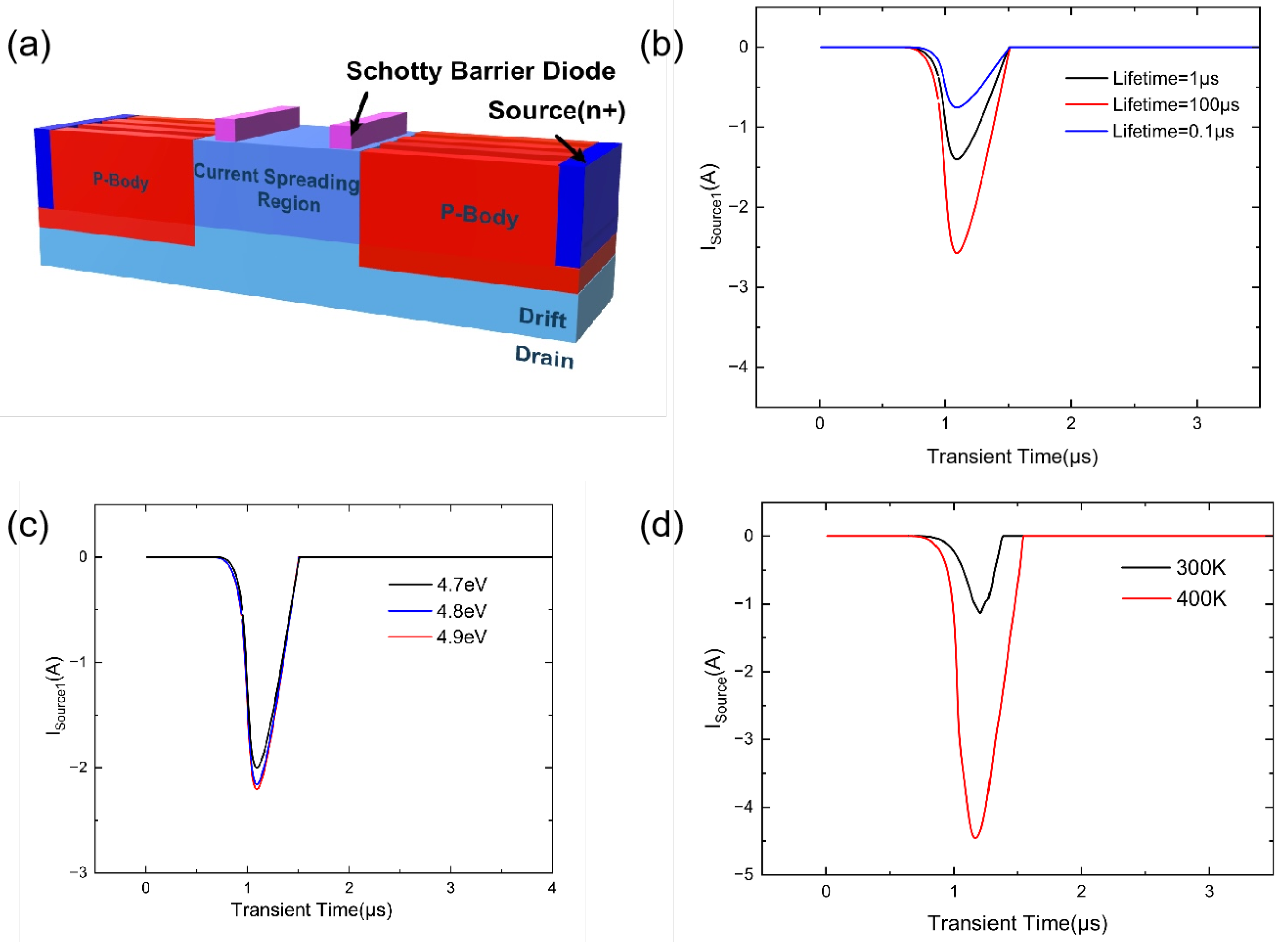
The schematic of the 3D view for SiC TED MOS, with and without SBD, is shown in Figure 1a,b, as well as the cross-section along two axes (Figure 1c,d). In this study, we explore the device characteristics within three trenched-etch channels, and SiC TED MOS with SBD is distinguished from the typical SiC TED MOS by depositing a parallel SBD on the source contact at the top of the current spreading region in a basic TED MOS structure. All device simulations and mix-mode simulation results were derived from simulations software Silvaco TCAD 2021 and the modeling process included defining meshes, regions, materials, electrodes, and doping concentration. The SiC TED MOS can be divided into the current drift region, current spreading region, left and right channels, and P-body region, where an ‘Atlas 3D’ module is necessary to establish a complete model. The parameters of SiC TED MOS are shown in Table 1. In this study, the TED MOS model with three channels is established, and, in order to further explore the influence of the newly-introduced SBD structure, we set the same parameters among all three structures, such as current scattering region concentrations, current drift region concentrations, n+source concentration, n-substrate concentration, and p-body concentration. By setting a reasonable mesh density, and allocating regions for all functional parts, a numerical solution method for TCAD is also essential. The isotherm drift–diffusion model requires the following three equations to be solved: electron concentration, potential, and hole concentration. It is of primary significance to perform calibration of the III-V compound semiconductor parameters and, fortunately, ‘atlas 3D’ is equipped with default 4H-SiC parameters, such as interface charge density, surface recombination velocity, dielectric permittivity, etc. Comparing these parameters with several research papers that include a Silvaco TCAD simulation, such as the work of Yagong Nan, Liao Yang, Kevin Matsui and so on [16,17,18,19,20], it was more reasonable to carry out the following simulation process.
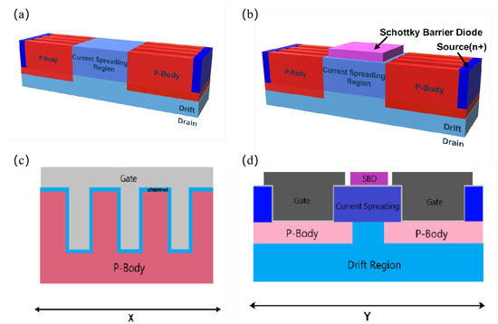
Figure 1.
Schematic of (a) 3D view of TED MOS without SBD; (b) 3D view of TED MOS with SBD; (c) cross-sectional view of TED MOS with SBD along the x-axis; (d) 3D view of TED MOS with SBD along the y-axis.

Table 1.
Key parameters for SiC TED MOS with SBD.
Various models were used before running static and dynamic simulations. The IMPACT SELB impact ionization model was used for activating avalanche breakdown simulations, and, in this study, we set gate voltage at two values (−5 V and 0 V) in breakdown tests to attain reverse breakdown voltage and forward breakdown voltage. The SRH was used for the carrier generation and recombination model. The FERMI was used for the fermi statistics model. The FLDMOB and ALBRCT were used to simulate the mobility and saturation velocity effects. The CALC.STRAIN was used to consider the strain. The POLARIZATION model was invoked for epitaxial strain due to lattice mismatch and spontaneous polarization. After setting up the suitable models, it was equally significant to choose computational methods and, for almost all cases, the NEWTON method was preferred, so it was the default in the static and dynamic simulations.
In dynamic simulations, during the forwarding turn-on simulations, the P-body region was under a forward voltage bias state, as well as the carriers inside the P-body region and current spreading region. When the device was switched off, the transverse field exhausted the carriers inside the body in a transverse manner, leaving the non-equilibrium carriers inside the device in a point and equilibrium state. After that, we could simulate the basic structure for SiC TED MOS, with and without SBD. Mix-mode simulation was utilized in exploring the DUTs test, to investigate the turn-on and reverse characteristics of three structures, as it is more feasible in setting up numerous circuit elements, like capacitance and inductance. It provides several valuable benefits as no compact model needs to be specified for a physically-based numerical device. In addition, approximation errors introduced by compact models can be avoided; particularly for large transient signal performance [21]. The DUTs test was conducted at an applied voltage of 300 V voltage, with a current source of 10 A applied and a reverse change rate of 100 A/s. There are other optional methods to set several parameters, such as temperature, carrier lifetime and work functions, which can obtain various device working conditions. Finally, the ‘Tonyplot’ module was utilized to plot the mix-mode simulation results and to visualize the electric field and capacitance distribution.
3. Results and Discussions
The drain current-gate voltage (I-V) characteristics of the test structures are plotted in Figure 2a,b. Figure 2a is a linear scale plot, while Figure 2b is in a log scale. Once the channel current reached 1 A, gate voltages could be extracted to compare the threshold voltage between the two devices. As the gate voltage increased, the TED MOS without SBD turned on when the gate voltage was equal to 5.23 V. There was a small difference between the TED MOS threshold and SBD (V = 5.43 V). After introducing the SBD structure, the threshold voltage increased, while the channel current decreased slightly, due to the expansion of gate-to-drain capacitance (C) and interface trap density between the current spreading region and the P-body region. Without an SBD structure, a thin oxide layer was deposited on the top of the current spreading region, so this oxide layer should be removed before defining a new SBD electrode. More carriers became trapped so a higher gate voltage was needed to activate the device. On the other hand, the channel mobility in a high electrical field decreased steeply because of the scattering factor in the high electric field. For example, extra metal deposition generates more scattering from surface roughness. Figure 2c illustrates the reverse breakdown voltage of the studied device under the condition that gate voltage (V) was −5 V, guaranteeing that all carriers were trapped, and Figure 2d depicts the forward breakdown voltage when the gate voltage was set to 0 V. All devices were under reverse voltage breakdown when drain voltage reached 1600 V and the forward breakdown voltage value achieved 1500 V. It was obvious that the SBD structure would not significantly change the limit of punch-through, as it is related to carrier concentration and channel properties. What is more, there was not much difference in the leakage current under the breakdown simulation, meaning that introducing an SBD structure did not deteriorate avalanche breakdown.
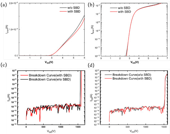
Figure 2.
(a) Transfer (I-V) of TED-MOS SiC, with or without the SBD structure, under the condition of V = 0.1 V on a linear scale; (b) Transfer (I-V) of TED-MOS SiC, with or without the SBD structure, under the condition of Vd = 0.1 V on a log scale; (c) The reverse breakdown simulation under the condition of V = −5 V (d) The forward breakdown simulation under the condition of V = 0 V.
In the current collapse simulation (Figure 3a), the SiC TED MOS, with and without the SBD structure, experienced circulation between on state and off state. Firstly, the gate voltage was set to 10 V to ensure that all carriers were extracted to the spreading channel, and the drain voltage was set to 1 V to drive the channel current. After 1ms, the device switched from on state to off state by altering the gate voltage to −5 V and boosting the drain voltage to 300 V. The peak channel current increased dramatically at 1 s, 4.48 × 10 A for the TED MOS with SBD and 4.32 × 10 A for the one without SBD, respectively. Once the device had been turned off for almost 1ms, on-state arrived when the transient time equaled 2 s by resetting all voltages to their initial values. The collapse current of the device with SBD was 2.36 × 10 A, while without SBD it only reached 2.06 × 10 A. This indicated the peculiarity that the SBD turns into a forward bias state when the device changes from the open state to an abrupt off state. The SBD helped to extract more carriers out from the P-Body region, leading to an augmentation of these properties. In Figure 3c three distinguished work functions were defined, with a drain voltage of 10 V and a gate voltage of 100 V, respectively. As the gate voltage decreased, leakage current could be plotted in a log scale plot. SiC TED MOS with SBD exhibited a significantly higher current density when compared to those without SBD, typically by two orders of magnitude. Nonetheless, an increase in the work function of the metal used in constructing the devices resulted in a reduction of the leakage current. The variation in the conduction band energy of the TED MOS devices with different work functions of the metals is depicted in Figure 3d, where it is evident that a higher work function of the metal resulted in a corresponding increase in the Schottky barrier height. The x-axis of Figure 3d is the vertical distance from the top SBD structure to the current spreading region and it is intuitive that, for example, the conduction band of the TED MOS with 4.9 eV metal work function was higher than that with 4.7 eV and 4.8 eV, hampering the carriers from spreading through the SBD structure. so less leakage could be seen. This phenomenon similarly affected the recovery characteristic of the devices with different work functions.
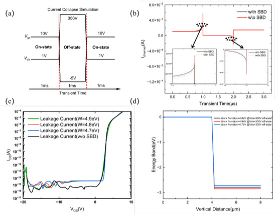
Figure 3.
(a) Timings and parameter settings in the current collapse simulation; (b) Current collapse results; (c) Leakage current under DUTs test; (d) Conduction band energy of SiC TED MOS with distinct work functions.
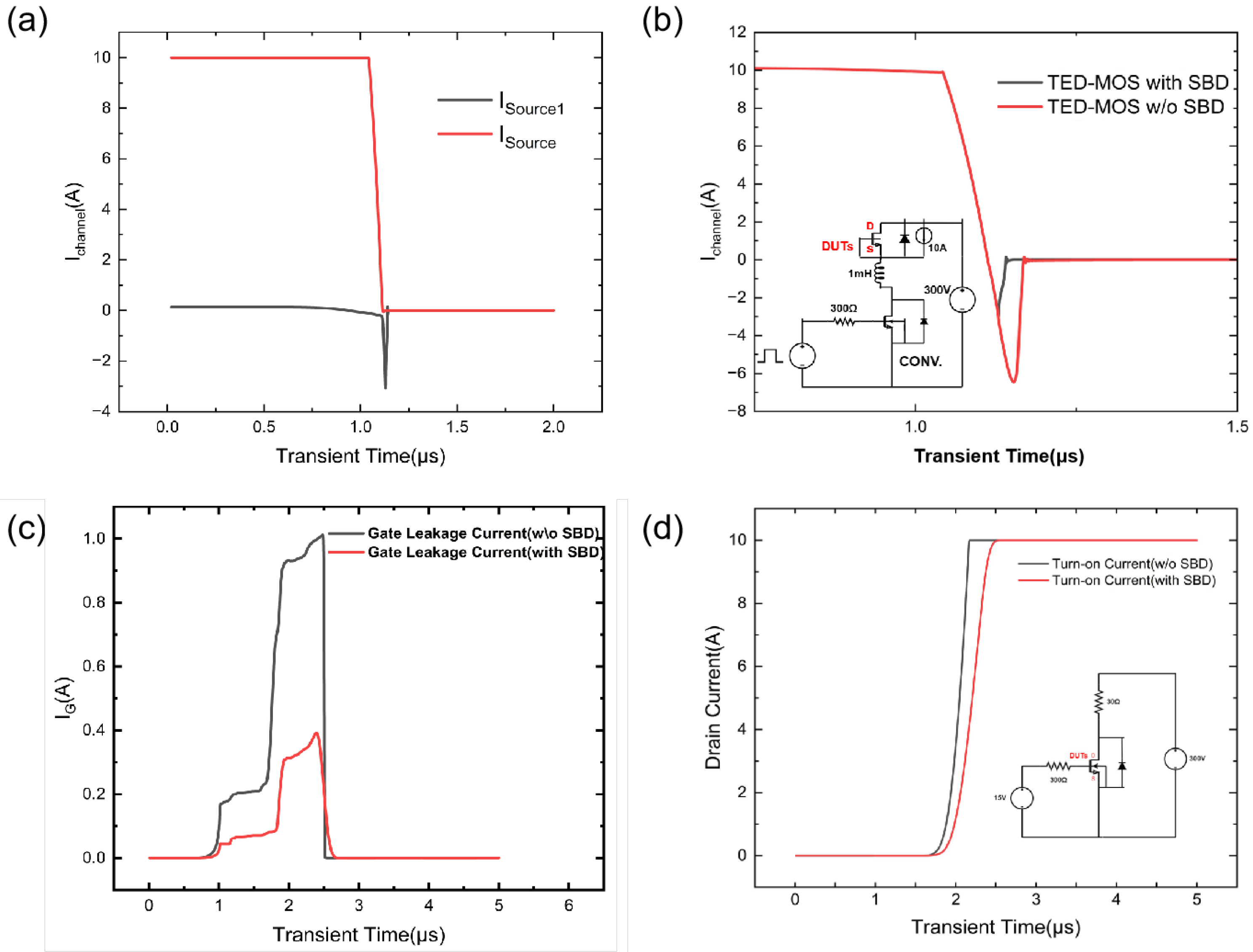
Figure 4a demonstrates the source and source1 currents under the condition that the work function of SBD equaled 4.8 eV. The newly introduced SBD structure was attained by depositing an additional electrode, called source1, and, when calculating the recovery current (I), both I and I should be taken into account as a whole. The reverse recovery characteristics of the SiC TED MOSFET devices ultimately depend on the parasitic diode, which becomes a forward bias state and extracts the stored charge when the device changes from on state to off state. It was evident that, in the DUTs test, when the whole device turned on at the beginning, the current mainly flowed through the source electrode. When circuits were switched off, the primary current in the SiC TED MOS was the main current generated by the source1 conduction. This means that the new SBD structure can work as a fly-back diode.

Figure 4.
(a) Two reverse recovery currents of SiC TED MOS with SBD (b) Total reverse recovery current of SiC TED MOS with SBD; (c) Leakage current under DUTs test; (d) Turn-on characteristic of studied SiC TED MOS.
Figure 4b illustrates the reverse recovery current, which was added by source1 and the source current. The inset illustrates the test circuit configuration, wherein the device under test (DUT) and the current transformation rate di/dt were set to 100 A/us by setting RG = 300 and Conv-SJ-MOSFET (CONV.) to the low side switch. The resistance played the part of circuit switch. After adding an SBD structure, the t descended significantly, and the I achieved 3.08 A, which was reduced by 52.2% for Si TED MOS (6.45 A), the Q attained 1.76 C, which decreased by 53.8% for Si SJ (3.81 C). It is cogent that the introduction of an SBD structure could apparently augment the reverse recovery characteristics.
The leakage gate current is shown in Figure 4c, explaining that a high Schottky barrier height could restrain it, and the DUTs test for the turn-on circuits indicated a gap between SiC TED MOS, with and without SBD (Figure 4d). After applying the SBD structure, the aggrandizement in the contact area between the gate and the drift region caused an enhancement in the gate-to-drain capacitance C. Due to its increased capacitance, the charging time for SiC TED MOS was prolonged and had a slight side effect for transmission, but this loss was not particularly appreciable, as more benefits could be gained in the recovery characteristics.
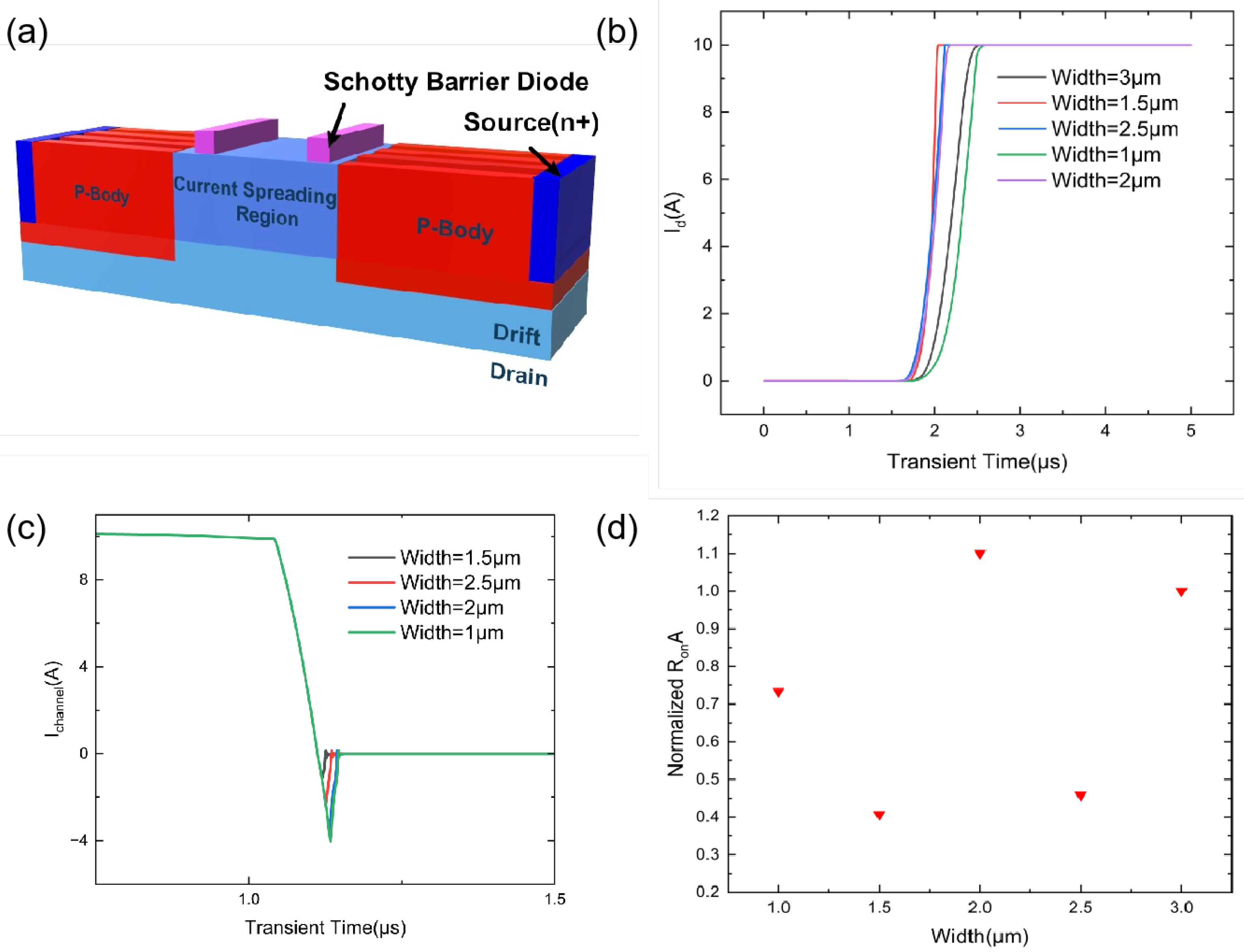
In order to explore more optimized structures, we split the entire SBD structure into two crosswise region transverse SBD structures (Figure 5) and probed into the optimal size for these. In the Figure 5a, these two structures did not change their lengths along the x-axis, while the variable was the width along the y-axis, and they covered most of the area near the top, side, and bottom channels to draw carriers out of the device as much as possible under reverse recovery simulation. Several distinct widths for two SBD structures were simulated under the DUTs test, and their turn-on characteristics are shown in Figure 5b with the 4.8 eV work function. It can be observed in the second inset, that the coverage area of the newly-introduced SBD structure proved to be the essential factor, as the transient time for all test structures had a gap and there was a marginal effect of optimized SBD width. With a width of 1.5 m, the SBD had the lowest turn-on transmission time. Comparing the entire SBD structure in Figure 1b, the turn-on delay of the 1.5 m wide SBD structure was less than that of an unabridged SBD structure. This is because the gate-to-drain capacitance could be reduced without significantly reducing the channel current.
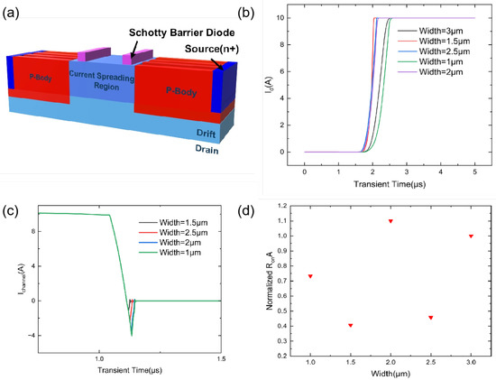
Figure 5.
(a) New SBD structure with two crosswise regions; (b) Turn-on performance with different SBD Widths; (c) Reverse recovery current with different SBD Widths; (d) Turn-on Normalized RA.
Figure 5c illustrates the same trend that was observed in the reverse recovery simulation. Similarly, the appropriate width lay in the middle range of variables. After using the innovative SBD structure, the t decreased more rapidly than it did for the basic SBD structure, and the I attained 1.13 A, which was a reduction of 82.5% for Si TED MOS (6.45 A), while the Q achieved 0.644 C, which was a reduction of 83.1% for Si SJ (3.81 C). For on resistance, we set the initial conditions of V = −5 V and V = 300 V to ensure that the carriers were sufficiently trapped in the traps. Then, the gate voltage changed to 15 V while the drain voltage decreased to 10 V. When the device switched from the off state to the on state for 100 s, the data was noted to calculate the on-state resistance. By setting the on-state resistance of the SBD structure (Width = 3 m) as 1, all studied structure data were as shown in Figure 5d. In conclusion, setting the SBD structure with width = 1.5 m obtained optimized device characteristics.
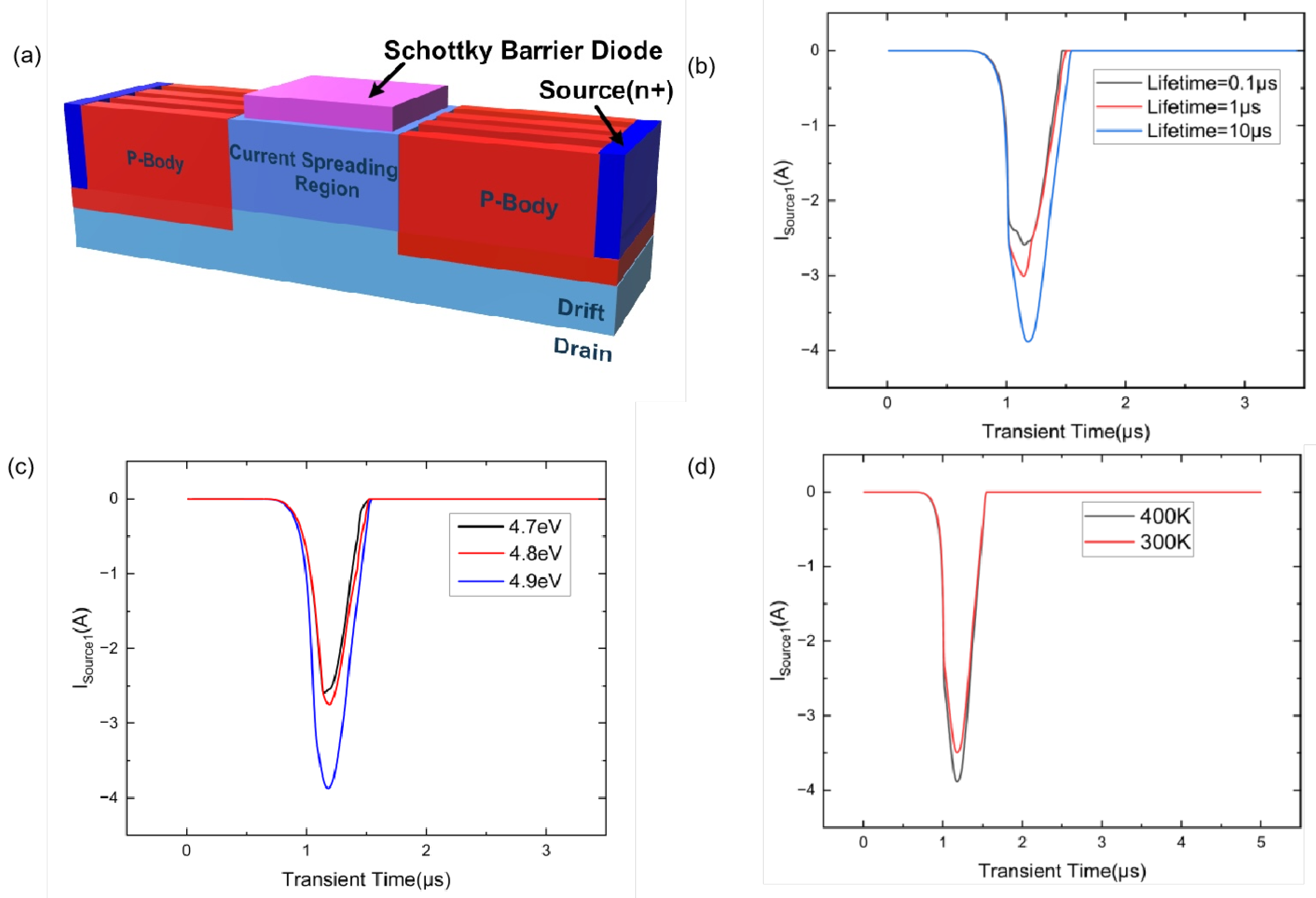
Three other factors were simulated (temperature, carrier lifetime, and work functions) during the DUTS reverse tests and the impact of the results on the I are shown in Figure 6. The structure in Figure 6a is described in Figure 1b and it is apparent that, with the aggrandizement of SBD work functions, the reverse recovery current experienced augmentation as well (Figure 3d). As the Schottky barrier became higher, fewer carriers were spread through it, as plotted in Figure 3d. In this situation, the higher work function was detrimental to the reverse recovery characteristic. As a result, less accumulated charge could be released and this negatively affected reverse recovery. Higher device temperature also had a side effect on the device because it impaired carrier mobility, making it more challenging to extract minor carriers from the device (Figure 3d). In Figure 6d, different carrier lifetimes were tested, and the conclusion drawn that carriers with higher lifetimes led to worse reverse recovery characteristics. The reason is that it takes longer for carriers with higher lifetimes to recombine, and it is harder to consume an accumulated charge, which accounts for the worse recovery characteristic.

Figure 6.
(a) Schematic view of basic SBD structure. Recovery characteristics with different (b) lifetimes, (c) work functions, and (d) temperatures.
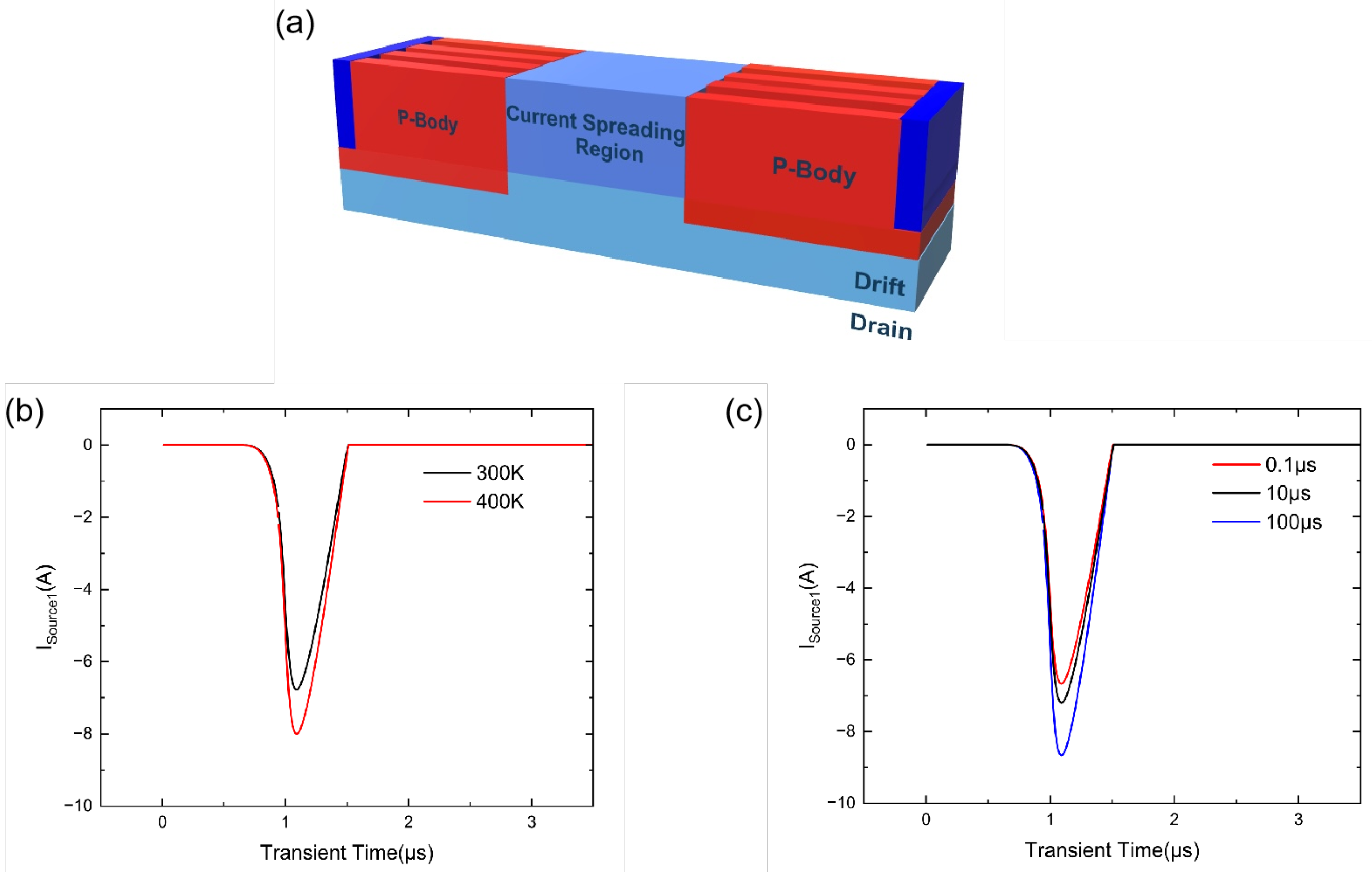
For the original SiC TED MOS, the structure in Figure 7a was the same as in Figure 1a, as it did not have an integrated SBD structure, and only the influences of temperature and carrier lifetime were investigated, seen in Figure 7b,c. The same trend could be drawn, since a similar mechanism applied, and it was more difficult for the device to have better reverse recovery characteristics under high temperature and carrier lifetime conditions. The SiC TED MOS with two transverse SBD structures was also explored for the effect of work function, temperature, and carrier lifetime. Figure 5a depicts the basic structure of Figure 8a, and, by examining Figure 8b–d, it can be deduced that temperature, carrier lifetime, and work functions each had an unique impact on the device’s recovery characteristics.
Figure 7.
(a) Schematic view of no SBD structure. Recovery characteristics with different (b) temperatures, and (c) lifetimes.
Figure 8.
(a) Schematic view of two crosswise SBD structures. Recovery characteristics with different (b) lifetimes, (c) work functions, and (d) lifetimes.
4. Conclusions
In this study, an integrated SBD structure in SiC TED MOS, devised for the purpose of improving reverse recovery characteristics, was demonstrated. The simulated results showed that its breakdown voltage, threshold voltage, and current collapse are acceptable, albeit with increased gate-to-drain capacitance. The SiC TED NOS with SBD decreased the I and Q by 52.2% and 53.8%, respectively, in comparison to the SiC TEDNOS without the SBD. Moreover, the depositing of two transverse SBD structures were more effective in recovery characteristics, and the I, Q of SiC declined by 82.5%, and 83.1%, compared to the SiC TED MOS without the SBD structure. In addition, three other factors, namely, temperature, work function, and carrier lifetime, were simulated. The tendency shows that the device prefers an appropriate temperature, low work function, and low carrier lifetime as more carriers are extracted under reverse circuits. The SiC TED MOS with the SBD structure can effectively aggrandize the switching speed and reduce switching loss in high-speed switching circuits.
Author Contributions
Conceptualization, H.C. and Q.W.; Data curation, H.C. and P.W.; Formal analysis, H.C. and W.L.; Funding acquisition, H.Y. and Q.W.; Investigation, H.C.; Methodology H.C. and W.L; Project administration, Q.W.; Resources, H.C. and W.L.; Software, H.C., P.W. and J.C.; Supervision, H.Y. and Q.W.; Validation, W.L.; Writing—original draft, H.C.; Writing—review & editing, W.L. and Q.W. All authors have read and agreed to the published version of the manuscript.
Funding
This research was funded by the Shenzhen Science and Technology Program (No. JSGG2022 0831094404008) and grants from the Guangdong Key Research and Development Program of China (2019B010143001). Fabrication of Normally-Off GaN Devices were based on in-situ SiNx Passivation and Selective Area Growth Recessed-Gate Techniques and the Reliability Study (National Natural Science Foundation of China, Grant No: 62274082), Research on novelty low-resistance Source/Drain ohmic contact for GaN p-FET (Grant No. JCYJ20220530115411025), Research on the Fabrication and Mechanism of GaN power and RF devices (Grant No. JCYJ20200109141233476), Research on the GaN Chip for 5G Applications (Grant No. JCYJ20210324120409025), Research on High-reliable GaN Power Device and Related Industrial Power System (Grant No. HZQB-KCZYZ-2021052) and Special Funds for the Cultivation of Guangdong College Students’ Scientific and Technological Innovation. (“Climbing Program” Special Funds) pdjh2023c21501. The authors acknowledge the assistance of SUSTech Core Research Facilities.
Data Availability Statement
The data presented in this study are available on request from the corresponding author.
Conflicts of Interest
The authors declare no conflict of interest. The funders had no role in the design of the study, in the collection, analyses, or interpretation of data, in the writing of the manuscript, or in the decision to publish the results.
References
- Agarwal, A.K.; Casady, J.B.; Rowland, L.B.; Valek, W.F.; White, M.H.; Brandt, C.D. 1.1 kV 4H-SiC power UMOSFETs. IEEE Electron Device Lett. 1997, 18, 586–588. [Google Scholar] [CrossRef]
- Li, Y.; Cooper, J.A.J.; Capano, M.A. High-voltage (3 kV) UMOSFETs in 4H-SiC. IEEE Trans. Electron Devices 2002, 49, 972–975. [Google Scholar] [CrossRef]
- Howell, R.S.; Buchoff, S.; Van Campen, S.; McNutt, T.; Ezis, A.; Nechay, B.; Kirby, C.; Sherwin, M.E.; Clarke, R.C.; Singh, R.V. A 10-kV Large-Area 4H-SiC Power DMOSFET With Stable Subthreshold Behavior Independent of Temperature. IEEE Trans. Electron Devices 2008, 55, 1807–1815. [Google Scholar] [CrossRef]
- Tega, N.; Yoshimoto, H.; Hisamoto, D.; Watanabe, N.; Shimizu, H.; Sato, S.; Mori, Y.; Ishigaki, T.; Matsumura, M.; Konishi, K.; et al. Novel trench-etched double-diffused SiC MOS (TED MOS) for overcoming tradeoff between RonA and Qgd. In Proceedings of the 2015 IEEE 27th International Symposium on Power Semiconductor Devices & IC’s (ISPSD), Hong Kong, China, 10–14 May 2015; pp. 81–84. [Google Scholar] [CrossRef]
- Tega, N.; Hisamoto, D.; Shima, A.; Shimamoto, Y. Channel Properties of SiC Trench-Etched Double-Implanted MOS (TED MOS). IEEE Trans. Electron Devices 2016, 63, 3439–3444. [Google Scholar] [CrossRef]
- Tega, N.; Tani, K.; Hisamoto, D.; Shima, A. Robustness improvement of short-circuit capability by SiC trench-etched double-diffused MOS (TED MOS). In Proceedings of the 2018 IEEE 30th International Symposium on Power Semiconductor Devices and ICs (ISPSD), Chicago, IL, USA, 13–17 May 2018; pp. 439–442. [Google Scholar] [CrossRef]
- Hino, S.; Hatta, H.; Sadamatsu, K.; Nagahisa, Y.; Yamamoto, S.; Iwamatsu, T.; Yamamoto, Y.; Imaizumi, M.; Nakata, S.; Yamakawa, S. Demonstration of SiC-MOSFET Embedding Schottky Barrier Diode for Inactivation of Parasitic Body Diode. In Materials Science Forum; Trans Tech Publications Ltd.: Stafa-Zurich, Switzerland, 2017; pp. 477–482. [Google Scholar]
- Kono, H.; Asaba, S.; Ohashi, T.; Ogata, T.; Furukawa, M.; Sano, K.; Yamaguchi, M.; Suzuki, H. Improving the specific on-resistance and short-circuit ruggedness tradeoff of 1.2-kV-class SBD-embedded SiC MOSFETs through cell pitch reduction and internal resistance optimization. In Proceedings of the 2021 33rd International Symposium on Power Semiconductor Devices and ICs (ISPSD), Nagoya, Japan, 30 May–3 June 2021; pp. 227–230. [Google Scholar] [CrossRef]
- Kawahara, K.; Hino, S.; Sadamatsu, K.; Nakao, Y.; Yamashiro, Y.; Yamamoto, Y.; Iwamatsu, T.; Nakata, S.; Tomohisa, S.; Yamakawa, S. 6.5 kV Schottky-Barrier-Diode-Embedded SiCMOSFET for Compact Full- Unipolar Module. In Proceedings of the 2017 29th International Symposium on Power Semiconductor Devices and IC’s (ISPSD), Sapporo, Japan, 28 May–1 June 2017; pp. 41–44. [Google Scholar]
- Nakashima, J.I.; Fukumoto, A.; Obiraki, Y.; Oi, T.; Mitsui, Y.; Nakatake, H.; Toyoda, Y.; Nishizawa, A.; Kawahara, K.; Hino, S.; et al. 6.5-kV Full SiC Power Module (HV100) with SBD-embedded SiC- MOSFETs. In Proceedings of the PCIM Europe 2018; International Exhibition and Conference for Power Electronics, Intelligent Motion, Renewable Energy and Energy Management, Nuremberg, Germany, 5–7 June 2018; pp. 441–447. [Google Scholar]
- Gao, R.; Cheng, H.; Li, W.; Deng, C.; Chen, J.; Wang, Q.; Yu, H. A Fast Recovery Vertical Superjunction MOSFET with n-Si and p-3C-SiC Pillars. Crystals 2022, 12, 916. [Google Scholar] [CrossRef]
- Li, S.; Li, A.; Tian, T.; Zhu, J.; Zhang, L.; Sun, W.; Zhu, G.; Zou, Y.; Tong, X.; Lu, Y.; et al. An Ultra-Low Qrr Cell-Distributed Schottky Contacts SJ-MOSFET with Integrated Isolated NMOS. In Proceedings of the 2019 31st International Symposium on Power Semiconductor Devices and ICs (ISPSD), Shanghai, China, 19–23 May 2019; pp. 479–482. [Google Scholar]
- Ebihara, Y.; Ichimura, A.; Mitani, S.; Noborio, M.; Takeuchi, Y.; Mizuno, S.; Yamamoto, T.; Tsuruta, K. Deep-P encapsulated 4H-SiC trench MOSFETs with ultra low R on Q gd. In Proceedings of the 2018 IEEE 30th International Symposium on Power Semiconductor Devices and ICs (ISPSD), Chicago, IL, USA, 13–17 May 2018; pp. 44–47. [Google Scholar]
- Xia, Y.; Chen, W.; Sun, R.; Liu, C.; Li, Z.; Zhang, B. A High Voltage Superjunction MOSFET with Enhanced Reverse Recovery Performance. In Proceedings of the 2021 5th IEEE Electron Devices Technology & Manufacturing Conference (EDTM), Chengdu, China, 8–11 April 2021; pp. 1–3. [Google Scholar]
- Han, Z.; Bai, Y.; Chen, H.; Li, C.; Lu, J.; Yang, C.; Yao, Y.; Tian, X.; Tang, Y.; Song, G.; et al. A Novel 4H-SiC Trench MOSFET Integrated With Mesa-Sidewall SBD. IEEE Trans. Electron Devices 2021, 68, 192–196. [Google Scholar] [CrossRef]
- Nan, Y.; Han, G. 4H–SiC floating junction Schottky barrier diode with compensation layer of engineered cathode structure: Cone-shaped electric field, current density waveform, and applications. Microelectron. J. 2022, 125, 105472. [Google Scholar] [CrossRef]
- Yoon, J.; Na, J.; Kim, K. A 1.2 kV SiC MOSFET with Integrated Heterojunction Diode and P-shield Region. Energies 2021, 14, 8582. [Google Scholar] [CrossRef]
- Matsui, K.; Tawara, T.; Harada, S.; Tanaka, S.; Sato, H.; Yano, H.; Iwamuro, N. Significant Improvement of Switching Characteristics in a 1.2-kV SiC SWITCH-MOS by the Application of Kelvin Source Connection. IEEJ Trans. Electr. Electron. Eng. 2022, 18, 278–285. [Google Scholar] [CrossRef]
- Yang, L.; Bai, Y.; Li, C.; Yang, C.; Chen, H.; Tang, Y.; Hao, J.; Tian, X.; Liu, X. Gate Oxide Instability of 4H-SiC p-Channel MOSFET Induced by AC Stress at 200 °C. IEEE Trans. Electron Devices 2023, 70, 379–382. [Google Scholar] [CrossRef]
- Li, P.; Ma, R.; Shen, J.; Jing, L.; Guo, J.; Lin, Z.; Hu, S.; Shi, C.; Tang, F. A Novel SiC MOSFET With a Fully Depleted P-Base MOS-Channel Diode for Enhanced Third Quadrant Performance. IEEE Trans. Electron Devices 2022, 69, 4438–4443. [Google Scholar] [CrossRef]
- ATLAS User’s Manual; Silvaco Int.: Santa Clara, CA, USA, 2010.

Disclaimer/Publisher’s Note: The statements, opinions and data contained in all publications are solely those of the individual author(s) and contributor(s) and not of MDPI and/or the editor(s). MDPI and/or the editor(s) disclaim responsibility for any injury to people or property resulting from any ideas, methods, instructions or products referred to in the content. |
© 2023 by the authors. Licensee MDPI, Basel, Switzerland. This article is an open access article distributed under the terms and conditions of the Creative Commons Attribution (CC BY) license (https://creativecommons.org/licenses/by/4.0/).