Article

Synthesis of Samarium Nitride Thin Films on Magnesium Oxide (001) Substrates Using Molecular Beam Epitaxy

1
Condensed Matter and Materials Physics, Idaho National Laboratory, Idaho Falls, ID 83401, USA
2
Center for Quantum Actinide Science and Technology, Idaho National Laboratory, Idaho Falls, ID 83401, USA
3
Materials and Fuels Complex, Idaho National Laboratory, Idaho Falls, ID 83401, USA
*
Author to whom correspondence should be addressed.
Crystals 2024, 14(9), 765; https://doi.org/10.3390/cryst14090765
Submission received: 2 August 2024 / Revised: 24 August 2024 / Accepted: 26 August 2024 / Published: 28 August 2024
(This article belongs to the Special Issue Materials and Devices Grown via Molecular Beam Epitaxy)

Abstract

:
Rare-earth nitrides are an exciting family of materials with a wide variety of properties desirable for new physics and applications in spintronics and superconducting devices. Among them, samarium nitride is an interesting compound reported to have ferromagnetic behavior coupled with the potential existence of p-wave superconductivity. Synthesis of high-quality thin films is essential in order to manifest these behaviors and understand the impact that vacancies, structural distortions, and doping can have on these properties. In this study, we report the synthesis of samarium nitride monocrystalline thin films on magnesium oxide (001) substrates with a chromium nitride capping layer using molecular beam epitaxy (MBE). We observed a high-quality monocrystalline SmN film with matching orientation to the substrate, then optimized the growth temperature. Despite the initial 2 nm of growth showing formation of a potential samarium oxide layer, the subsequent layers showed high-quality SmN, with semiconducting behavior revealed by an increase in resistivity with decreasing temperature. These promising results highlight the importance of studying diverse heteroepitaxial schemes and open the door for integration of rare-earth nitrides and transition metal nitrides for future spintronic devices.

1. Introduction

Rare-earth nitrides (RENs) are an exciting family of materials with a wide variety of properties desirable in the fields of spintronics, infrared detectors, intrinsically ferromagnetic-based tunnel junctions, and strongly correlated electron materials [1]. The electronic configuration of elements containing 4f orbitals is a source of interesting new physics; as an example, samarium nitride (SmN) has been reported to support the coexistence of semiconductor behavior, ferromagnetic states, and superconductivity [2].
Interest in SmN has been growing since the first reports of its magnetic properties [3]. After a few quiet years, interest began to increase with the reported optimization of computational models for RENs with experimental feedback studies on dysprosium nitride (DyN) and SmN [4]. This was followed by a study in which ferromagnetism in SmN was identified below 27 K and attributed to the spin and orbital moments of the ground state of the Sm3+ ion [5]. The unusual coexistence of superconductivity was discovered to be a result of the N vacancies in the structure, which generate a large exchange splitting of the conduction band favoring equal spin-triplet pairing with p-wave symmetry [2]. Shortly afterwards, the anomalous Hall effect was reported in SmN and correlated to its nature as a heavy-fermion 4f conduction band material [6]. The band gap of SmN was identified to be 1.2 eV in [7] and 1.27 eV in [8]. Optical absorption measurements further confirmed the existence of n-type doping through N vacancies [9]. These results highlight the fact that physical properties of SmN thin films are dependent on synthesis conditions. In addition to these experimental efforts to determine the properties of SmN, several density functional theory studies have investigated its magnetic structure [10,11,12], structural and electronic properties [13,14], phase transitions [13,15], and resonance modes [16].
In order to better understand the properties of SmN, high quality samples are paramount. SmN has been synthesized using high vacuum evaporation, pulsed laser deposition (PLD), and MBE. Sample quality is heavily dependent on synthesis technique; even within the same technique, growth conditions heavily influence the result. Growth with PLD has yielded highly textured films [17], while evaporation under ultra-high vacuum conditions has produced films from polycrystalline to epitaxial [5,6,18,19] and MBE is known as the pinnacle of vapor deposition techniques, as demonstrated by its use in low-dimensional structures [20,21,22] and integration of dissimilar material systems [23,24,25] where high-quality and atomically precise layers of materials are achievable. MBE-deposited SmN films have been deposited on (0001)AlN, (0001)GaN, Si(001), and most recently LAO(001) [2,26,27,28,29,30]. Additionally, a number of particular growth peculiarities have been observed. Through a temperature-driven growth regime, SmN was reported to switch between (111)-oriented and (001)-oriented when grown on AlN [26], while the effects of varying the Sm and N flux on films deposited on fused silica and sapphire revealed a contraction of the lattice constant of polycrystalline films with N/RE flux decrease [31].
In this study, we present an analysis of the synthesis of SmN thin films on MgO(001) using molecular beam epitaxy. The lattice mismatch between the (001) planes of SmN and MgO is of 20.7% compressive strain, and a 45° rotation of the film with respect to the substrate yields only 14.4% tensile strain. Surprisingly, we discovered the epitaxial relation to occur on the larger lattice mismatch, in contrast with the reports on LAO where the film rotated 45°. Overcoming this large lattice mismatch could open the door for integration with new families of transition metal nitride materials, allowing for further enhancement of future spintronic applications.

2. Materials and Methods

Our samples were synthesized using a Veeco GenXplor plasma-assisted molecular beam epitaxy system with a base pressure of 2 × 10 10 Torr. No chemical treatment was used on the substrates, which were mounted onto sample holders using a 10 × 10 mm hole faceplate with Si backing wafer. The substrates were heated to 200 °C under a vacuum of <1 ×   10 7 Torr for two hours prior to introduction to the growth chamber. After the initial outgassing, the substrates were transferred to the growth chamber and heated to 800 °C in order to thermally clean the surface prior to cooling to the desired growth temperature. The growth temperatures were 540–740 °C, as measured by the black body radiation detected via a pyrometer and kSA BandiT system calibrated to the Si 7 × 7 reconstruction observed with reflection high energy electron diffraction (RHEED) and with the emissivity adjusted to match MgO. Sm was supplied from a standard effusion cell with a cell temperature of 545 °C, corresponding to a beam equivalent pressure of 5 × 10 8 Torr, providing a growth rate which was constant at all temperatures of 0.575 nm/min. To account for differences in effusion cell and substrate temperature that might cause Sm atom desorption, this was determined by ex situ thickness measurements. Nitrogen was supplied using a nitrogen plasma source with a mass flow of 3 sccm and a radio frequency power of 300 W. After completion of the SmN layer, all samples were capped with 6 nm of CrN grown at the same Tsub as the SmN layer (540 °C, 640 °C and 740 °C) to protect it from oxidation, followed by cooling the sample to room temperature under N plasma.
The initial structural symmetry and epitaxial quality were characterized using in situ RHEED with an electron beam of 15 kV and 14.2 A; the diffraction patterns indicate the quality of the sample’s surface. Structural characterization employed a Bruker D8 Advanced X-ray diffractometer using a Ge double-bounce monochromator and Cu K α 1 radiation ( λ = 1.5406 Å) with a power of 1600 W. Rocking curves, 2 θ - ω scans, and pole figures were used to study the crystal quality and structure of the samples. A conventional four-probe technique implemented in a Quantum Design DynaCool-14 physical property measurement system was used to investigate electrical resistivity from 2 K to 300 K and in magnetic fields up to 12 T on rectangular cleaved pieces of the samples of 2 × 6 mm. The results from these characterization techniques are discussed in the next section.

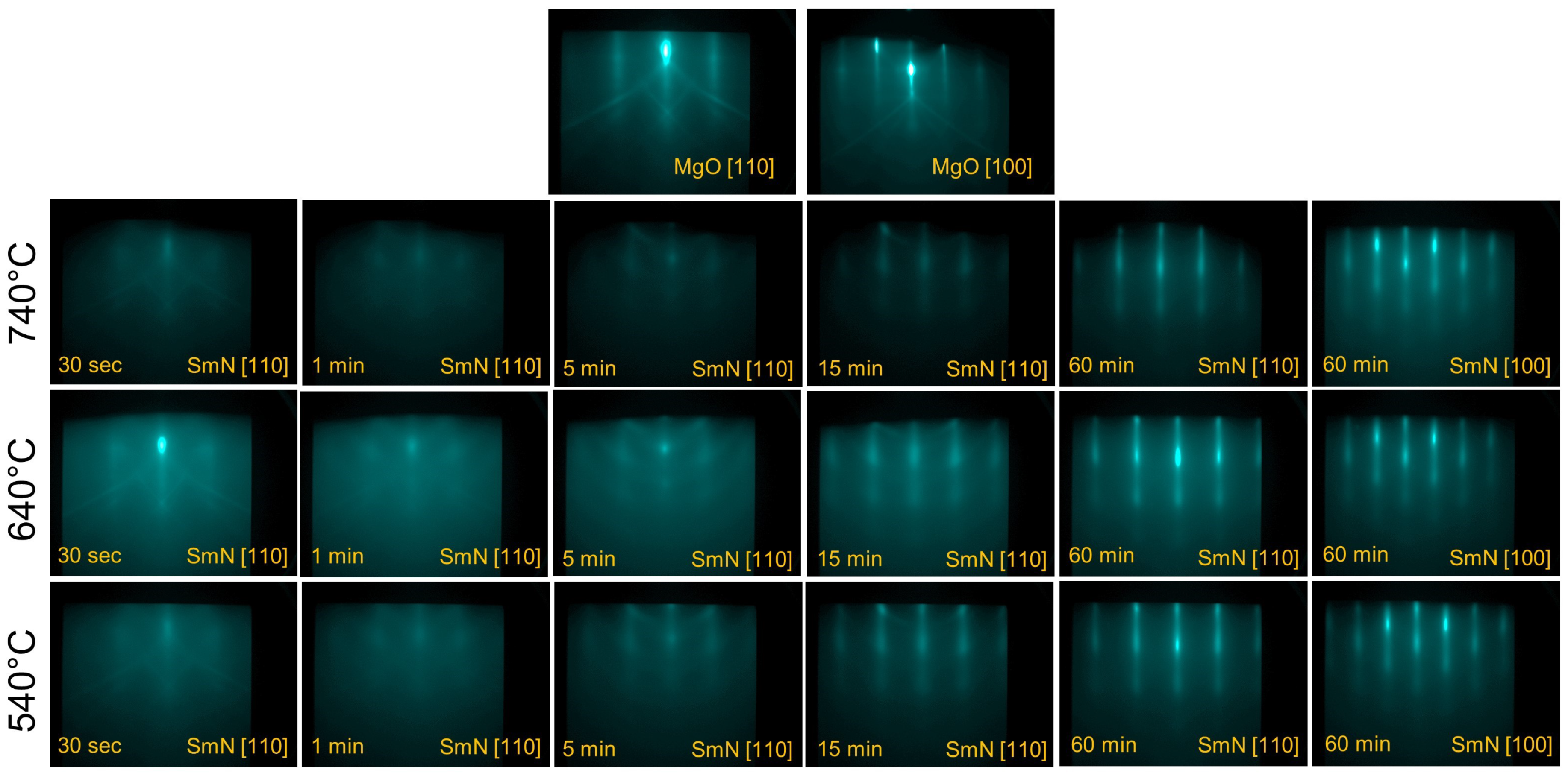
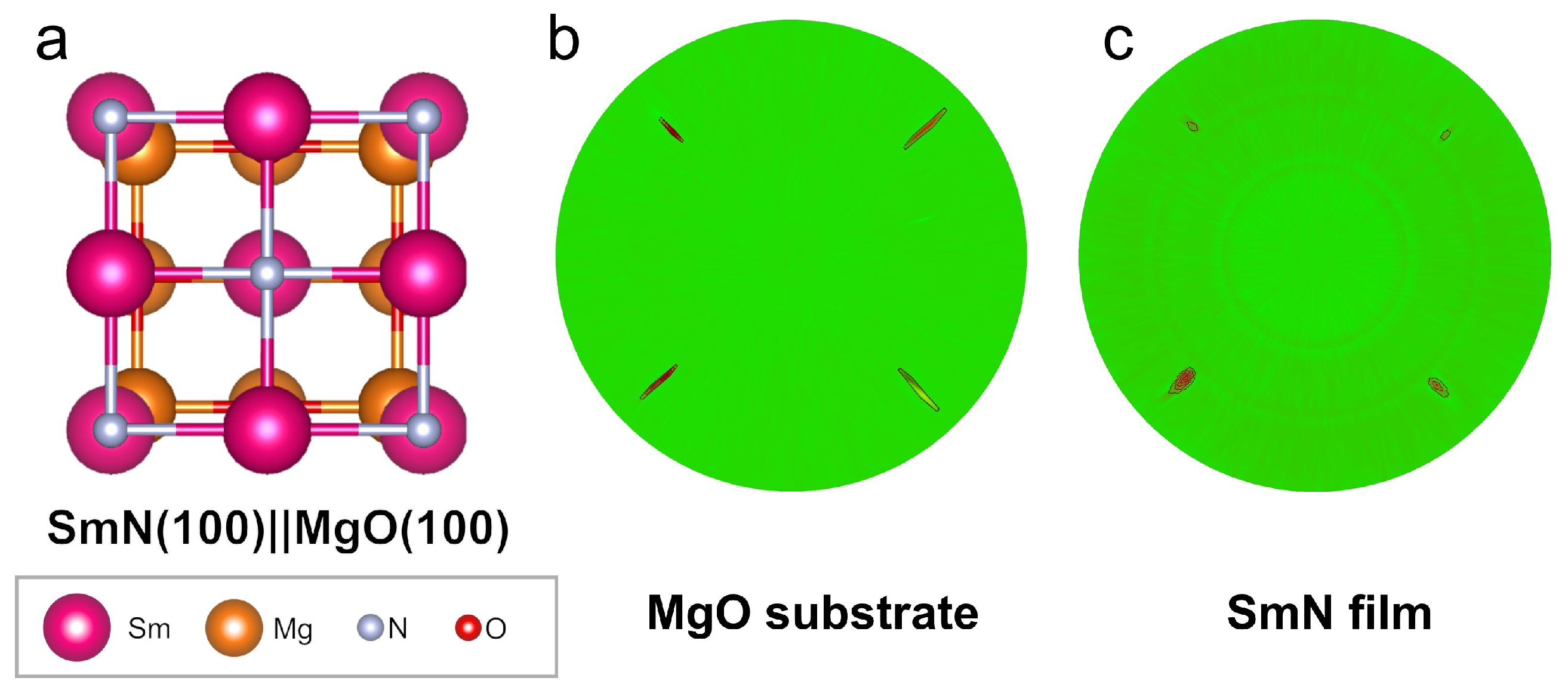
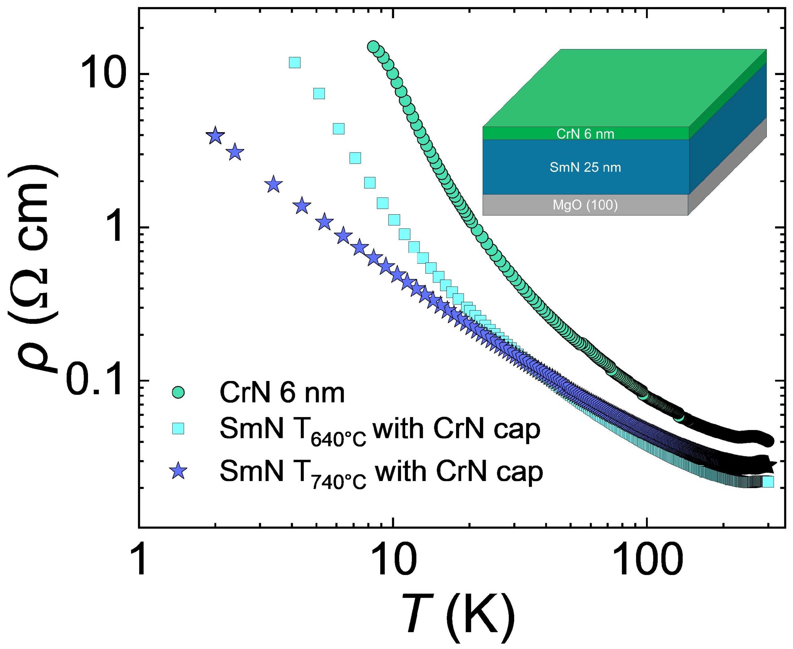
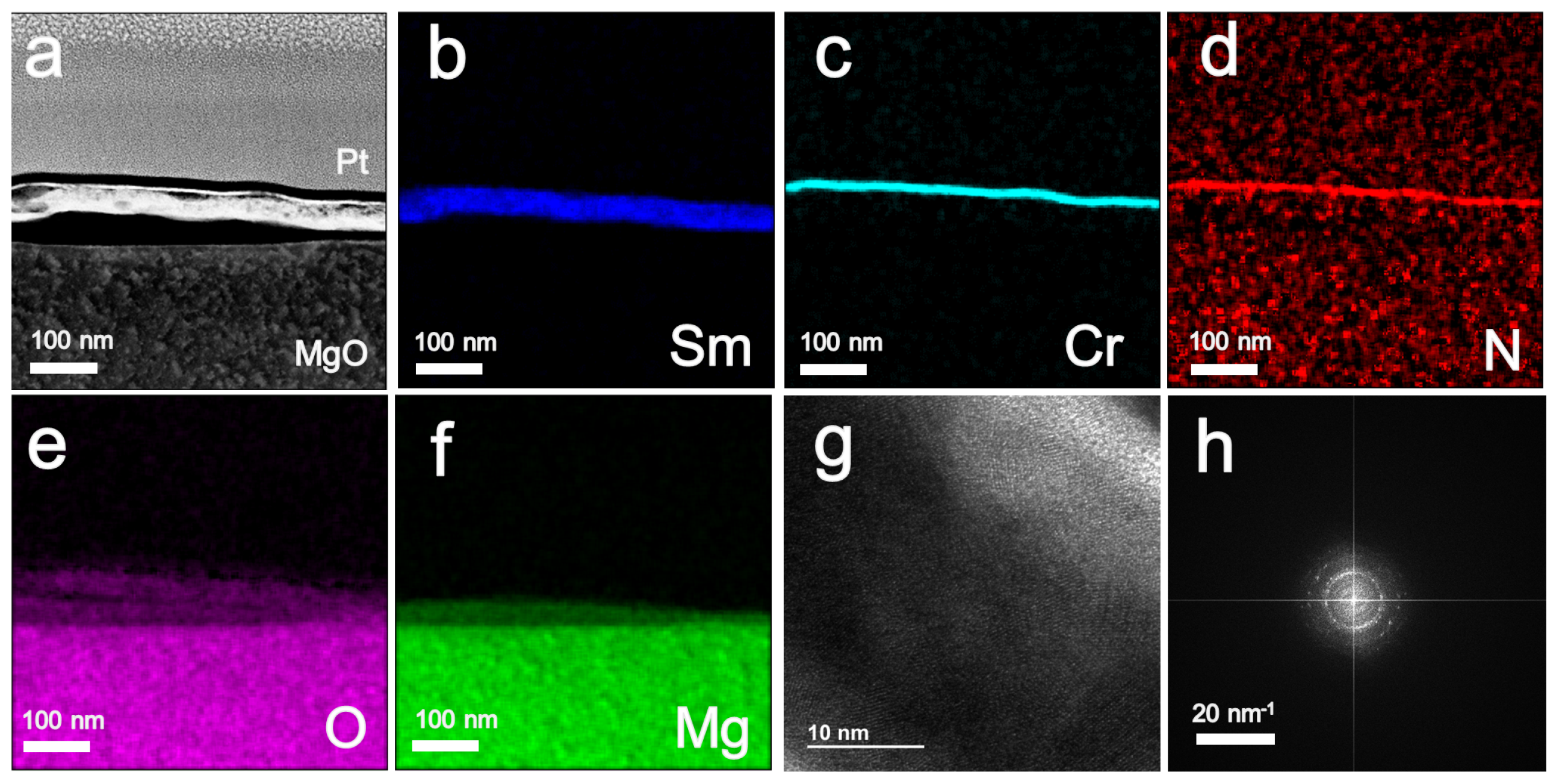
3. Results and Discussion

Figure 1 shows the evolution of the RHEED pattern for each sample grown at different Tsub. The RHEED patterns for all samples evolved following a similar pattern of dimming and reconstruction. During the first minute, considerable dimming occurs in the streaky pattern from the substrate. We attribute this either to formation of a samarium oxide at the interface with the oxide-based substrate surface or to the formation of strain-related defects along the interface [17], as the first couple of monolayers form in the first 52 s. Determining the exact mechanism proves difficult given the extreme air sensitivity of this material for oxidation; lanthanide materials are known to form stronger bonds with O and Si than with N [19]. During minutes 2 to 5 of growth, the pattern displays a reconstruction that hints at the formation of a rough surface, potentially through a reorganization of the surface to form the SmN (corresponding to monolayers 4–11 of growth). This pattern begins to give way to the formation of streaks during minutes 6 to 10 (13–23 monolayers), though there is still a degree of ring-like pattern present which steadily disappears as growth progresses. During minutes 10 to 60 (monolayers 23 to 68), a streaky pattern indicates the formation of a smooth surface with crystalline order. The sample was rotated 45° after the SmN layer was finished and the diffraction pattern was viewed along the <100> direction, revealing a RHEED pattern with spacing between the streaks corresponding to the expected 2 / 2 relation. This rotational symmetry is indicative of cubic symmetry on the part of the SmN film.
In order to help determine the epitaxial relationship between film and substrate, we measured the spacing between the RHEED streaks to extract the spacing between atomic planes. Using ImageJ software [32], a histogram was created from a slice on the same location in every RHEED pattern in Figure 1. Figure 2 shows the plot of the measured spacing between atomic planes as a function of the growth time. It can be seen that there is a considerable increase in the lattice constant (a reduction in the streak spacing in reciprocal space) followed by a gradual decrease towards a value of 3.57 Å. This value corresponds to the spacing between (110) planes on SmN; the lattice constant along the (001) planes is 5.084 Å, as calculated from Figure 1 [2]. Using the position of the SmN(200) reflection from the XRD pattern, the lattice constant is calculated to be 5.078 Å. This rapid change in lattice constant correlates with the dimming of the RHEED pattern observed during the initial stages of growth, further supporting the formation of a highly defective interface between substrate and film; this could result from oxidation, as previously reported in [17]. This effect could be reduced through implementation of buffer layers to lessen the chemical reactivity and the strain that must be accommodated at the substrate surface.
The thickness of this defective oxide layer is confined to the first few monolayers, as revealed by the X-ray diffraction patterns of all three samples showing only SmN and no evidence of samarium oxide compounds. Figure 3 shows that the only peaks present in addition to the substrate are those of SmN(002) and SmN(004); coupled with the spacing between atomic planes obtained in RHEED, this indicates an epitaxial relationship of SmN(001)<100>||MgO(001)<100> (Figure 4a). Interestingly, GdN has a similarly large lattice mismatch (18.6%) and has been found to grow in the same way on MgO(001) [33]. No peaks are observed which correspond to the CrN capping layer used for these samples, likely due to the CrN being very thin (6 nm) and having close lattice matching to the substrate, making the substrate peak look slightly asymmetrical (see Figure 3). Previous growths with the absence of a capping layer, which are not presented in this study, all showed the formation of samarium sesquioxide and monoxide phases (Sm2O3 and SmO) generated by the rapid oxidation of those samples, showing that CrN serves as an effective capping layer.
In order to confirm the epitaxial relationship of film and substrate, we performed texture goniometry through XRD pole figures. For the substrate, there are four sharp pole-density maxima at a tilt angle ( χ ) of 55°, with a constant angular distance of 90° in the azimuthal angle ( ϕ ) that characterizes the MgO{111} pole figure. Similarly, the SmN{111} pole figure for the CrN-capped SmN film exhibits four maxima at the same positions (tilt angle 55°). This supports the presence of a cube-on-cube epitaxy with the following, respective polar and azimuthal epitaxial relationships: SmN(100)||MgO(100) and SmN[100]||MgO[100]. The polar and azimuthal widths of the four SmN{111} pole-density maxima (1.1°–3°) are only slightly larger than those of the substrate (1°–1.5°), indicating a slight mosaic spread of the SmN crystallites in the films. The rocking curves of the SmN(200) for the epitaxial SmN films on MgO(100) have an FWHM of 0.572°.
Across the three different substrate temperatures studied in this paper, the highest growth temperatures yield the highest-quality films, as evidenced by the lowest substrate/film peak intensity ratio and smallest FWHM of 0.572° even with the large lattice mismatch (Figure 5). Further investigation of the morphology of the vacancies and crystal quality of SmN with respect to other growth parameters, such as the growth rate and N plasma power, are the subject of ongoing investigations.
Having confirmed the good crystal quality of the films, we investigated the electrical transport properties of the samples grown at Tsub = 740 °C and 640 °C (capped with CrN), finding them to show semiconducting behavior across the studied temperature range as evidenced by an increase in resistivity of roughly three orders of magnitude (see Figure 6). Around 274 K, there is evidence of the well-known CrN transition from a paramagnetic rock salt to an antiferromagnetic orthorhombic phase [34], indicating that our resistivity data originate in part from the CrN film. Thin CrN films have been reported to become resistive at low temperatures, in contrast to the metallic behavior exhibited by thicker films [34]. Given the nature of the metallic contacts on the samples (Al cables placed with a wire bonder), the penetration depth is larger than the thickness of the CrN capping layer; combined with a highly resistive substrate (MgO), this results in the data indicating semiconducting SmN. The residual resistivity ratio for this thin CrN layer is ρ 300 K / ρ 10 K = 0.004, while for SmN it is 0.0196 and 0.0570 for Tsub = 740 °C and 640 °C, respectively. The SmN films appear to be more conductive than the thin CrN, as expected from a measurement with parallel conduction channels given the negligible diffusion of CrN into SmN.
The absence of previously reported ferromagnetic transition and superconductive behavior can be attributed to a lack of VN, opening a path for future investigations on flux ratio conditions between Sm and N. The presence of dislocations, disorder, and defects could also contribute to the observed behavior. Magnetoresistance measurements showed no significant change in the resistance with the application of magnetic fields up to 13 T (at 20 K ≈ 0.3%).
In order to verify the crystal structure of the SmN film and its relationship with the substrate, we attempted to analyze it through transmission electron microscopy (TEM). During the sample preparation process for TEM, the cross-sectional surface of the foiled sample is exposed to atmosphere during the time it takes for the sample to be transported from the focused ion beam to the TEM (on the order of three minutes). Figure 7a shows a TEM micrograph of the film/substrate interface, while Figure 7b–f shows the corresponding EDS maps. The Sm is localized to a 34.55 nm region which appears to have partially delaminated from the substrate surface. Additionally, the area corresponding to the film appears to be polycrystalline, with large concentrations of oxygen. We believe that this happened during preparation of the TEM specimen, as the film did not appear to be oxidized or polycrystalline in the diffraction patterns discussed earlier (see Figure 1 and Figure 3). The CrN capping layer appears to remain in place and cover the entirety of the Sm-containing layer even after delamination from the substrate. Figure 7h shows the diffraction pattern of the SmN layer, where the presence of three distinct polycrystalline rings indicates three different atomic spacings (Figure 1 and Figure 3).

4. Conclusions

Despite their large lattice constant mismatch, SmN thin films can be grown using the epitaxial relation SmN(001)<100>||MgO(001)<100> via molecular beam epitaxy. By providing N plasma power of 300 W and Sm flux calibrated for a growth rate of 0.575 nm/min, we synthesized high-quality SmN thin films at a Tsub of 740 °C. These films exhibit semiconducting behavior with near-zero magnetoresistance. This successful integration of SmN with MgO substrates opens a new avenue of research into spintronic heterostructures and devices via epitaxial growth of transition metal nitrides and rare earth nitrides.

Author Contributions

Conceptualization, K.D.V. and K.G.; methodology, K.D.V., K.G. and B.J.M.; formal analysis, K.D.V., B.J.M., K.G., V.B. and Z.E.C.; investigation, B.S.N., K.D.V. and V.B.; resources, K.D.V. and K.G.; data curation, K.D.V.; writing—original draft preparation, K.D.V.; writing—review and editing, B.S.N., K.D.V., B.J.M., K.G., V.B. and Z.E.C.; project administration, K.D.V.; funding acquisition, K.D.V. All authors have read and agreed to the published version of the manuscript.

Funding

This work was supported through the INL Laboratory Directed Research and Development Program under the U.S. Department of Energy, Idaho Operations Office, Contract DE-AC07-05ID14517. K.D.V., B.J.M. and Z.E.C. acknowledge the support of the NNSA Minority Serving Institution Partnership Program (MSIPP).

Data Availability Statement

The raw data supporting the conclusions of this article will be made available by the authors on reasonable request.

Acknowledgments

K.D.V., B.J.M. and Z.E.C. acknowledge the Minority Serving Institution Partnership Program for their support. This work made use of the Nanofab EMSAL shared facilities of the Micron Technology Foundation Inc. Microscopy Suite sponsored by the John and Marcia Price College of Engineering, Health Sciences Center, Office of the Vice President for Research.

Conflicts of Interest

The authors declare no conflicts of interest.

References

  1. Natali, F.; Ruck, B.J.; Plank, N.O.; Trodahl, H.J.; Granville, S.; Meyer, C.; Lambrecht, W.R. Rare-earth mononitrides. Prog. Mater. Sci. 2013, 58, 1316–1360. [Google Scholar] [CrossRef]
  2. Anton, E.M.; Granville, S.; Engel, A.; Chong, S.V.; Governale, M.; Zülicke, U.; Moghaddam, A.G.; Trodahl, H.J.; Natali, F.; Vézian, S.; et al. Superconductivity in the ferromagnetic semiconductor samarium nitride. Phys. Rev. B 2016, 94, 024106. [Google Scholar] [CrossRef]
  3. Moon, R.; Koehler, W. Magnetic properties of SmN. J. Magn. Magn. Mater. 1979, 14, 265–269. [Google Scholar] [CrossRef]
  4. Preston, A.; Granville, S.; Housden, D.; Ludbrook, B.; Ruck, B.; Trodahl, H.; Bittar, A.; Williams, G.; Downes, J.; DeMasi, A.; et al. Comparison between experiment and calculated band structures for DyN and SmN. Phys. Rev. B Condens. Matter Mater. Phys. 2007, 76, 245120. [Google Scholar] [CrossRef]
  5. Anton, E.M.; Ruck, B.J.; Meyer, C.; Natali, F.; Warring, H.; Wilhelm, F.; Rogalev, A.; Antonov, V.N.; Trodahl, H.J. Spin/orbit moment imbalance in the near-zero moment ferromagnetic semiconductor SmN. Phys. Rev. B Condens. Matter Mater. Phys. 2013, 87, 134414. [Google Scholar] [CrossRef]
  6. Holmes-Hewett, W.F.; Ullstad, F.H.; Ruck, B.J.; Natali, F.; Trodahl, H.J. Anomalous Hall effect in SmN: Influence of orbital magnetism and 4f -band conduction. Phys. Rev. B 2018, 98, 235201. [Google Scholar] [CrossRef]
  7. Azeem, M. On the optical energy gap of SmN. Chin. J. Phys. 2018, 56, 1925–1930. [Google Scholar] [CrossRef]
  8. Holmes-Hewett, W.F.; Buckley, R.G.; Ruck, B.J.; Natali, F.; Trodahl, H.J. Optical spectroscopy of SmN: Locating the 4f conduction band. Phys. Rev. B 2019, 99, 205131. [Google Scholar] [CrossRef]
  9. Azeem, M. Quantitative measure of nitrogen vacancy related effects in SmN and EuN. Adv. Nat. Sci. Nanosci. Nanotechnol. 2019, 10, 015003. [Google Scholar] [CrossRef]
  10. Morari, C.; Beiuşeanu, F.; Marco, I.D.; Peters, L.; Burzo, E.; Mican, S.; Chioncel, L. Magnetism and electronic structure calculation of SmN. J. Phys. Condens. Matter 2015, 27, 115503. [Google Scholar] [CrossRef] [PubMed]
  11. McNulty, J.F.; Ruck, B.J.; Trodahl, H.J. On the ferromagnetic ground state of SmN. Phys. Rev. B 2016, 93, 054413. [Google Scholar] [CrossRef]
  12. Som, N.N.; Mankad, V.H.; Dabhi, S.D.; Patel, A.; Jha, P.K. Magnetic behavior study of samarium nitride using density functional theory. J. Magn. Magn. Mater. 2018, 448, 186–191. [Google Scholar] [CrossRef]
  13. Aynyas, M.; Panwar, Y.S.; Pataiya, J.; Makode, C.; Sanyal, S.P. Properties of samarium nitride: First principle calculations. AIP Conf. Proc. 2016, 1728, 020015. [Google Scholar] [CrossRef]
  14. Holmes-Hewett, W.F. Electronic structure of nitrogen-vacancy doped SmN: Intermediate valence and 4f transport in a ferromagnetic semiconductor. Phys. Rev. B 2021, 104, 075124. [Google Scholar] [CrossRef]
  15. Hao, A.M.; Bai, J.; Luo, S.H.; Qi, X.W. First Principles Investigation of Electronic Property and High Pressure Phase Stability of SmN. Chin. J. Chem. Phys. 2016, 29, 219–222. [Google Scholar] [CrossRef]
  16. Holmes-Hewett, W.F.; Buckley, R.G.; Butler, T.J.; Pot, C.; Koughnet, K.V.; Ruck, B.J.; Trodahl, H.J. TO(Γ) mode resonances in the rare-earth nitrides. AIP Adv. 2022, 12, 075120. [Google Scholar] [CrossRef]
  17. Natali, F.; Ludbrook, B.; Galipaud, J.; Plank, N.; Granville, S.; Preston, A.; Do, B.L.; Richter, J.; Farrell, I.; Reeves, R.; et al. Epitaxial growth and properties of GdN, EuN and SmN thin films. Phys. Status Solidi (C) Curr. Top. Solid State Phys. 2012, 9, 605–608. [Google Scholar] [CrossRef]
  18. McNulty, J.F.; Anton, E.M.; Ruck, B.J.; Natali, F.; Warring, H.; Wilhelm, F.; Rogalev, A.; Soares, M.M.; Brookes, N.B.; Trodahl, H.J. Twisted phase of the orbital-dominant ferromagnet SmN in a GdN/SmN heterostructure. Phys. Rev. B Condens. Matter Mater. Phys. 2015, 91, 174426. [Google Scholar] [CrossRef]
  19. McNulty, J.F.; Temst, K.; Bael, M.J.V.; Vantomme, A.; Anton, E.M. Epitaxial growth of (100)-oriented SmN directly on (100)Si substrates. Phys. Rev. Mater. 2021, 5, 113404. [Google Scholar] [CrossRef]
  20. Petroff, P.M.; Lorke, A.; Imamoglu, A. Epitaxially self-assembled quantum dots. Phys. Today 2001, 54, 46–52. [Google Scholar] [CrossRef]
  21. Vallejo, K.D.; Cabrera-Perdomo, C.I.; Garrett, T.A.; Drake, M.D.; Liang, B.; Grossklaus, K.A.; Simmonds, P.J. Tunable mid-infrared interband emission from tensile-strained InGaAs quantum dots. ACS Nano 2023, 17, 2318–2327. [Google Scholar] [CrossRef]
  22. Vallejo, K.D.; Garrett, T.A.; Cabrera, C.I.; Liang, B.; Grossklaus, K.A.; Simmonds, P.J. Tensile-strained self-assembly of InGaAs on InAs (111) A. J. Vac. Sci. Technol. B 2021, 39, 062809. [Google Scholar] [CrossRef]
  23. Haidet, B.B.; Nordin, L.; Muhowski, A.J.; Vallejo, K.D.; Hughes, E.T.; Meyer, J.; Simmonds, P.J.; Wasserman, D.; Mukherjee, K. Interface structure and luminescence properties of epitaxial PbSe films on InAs (111) A. J. Vac. Sci. Technol. A Vac. Surf. Film. 2021, 39, 023404. [Google Scholar] [CrossRef]
  24. May, B.J.; Sarwar, A.; Myers, R.C. Nanowire LEDs grown directly on flexible metal foil. Appl. Phys. Lett. 2016, 108, 141103. [Google Scholar] [CrossRef]
  25. May, B.J.; Hettiaratchy, E.C.; Wang, B.; Selcu, C.M.; Esser, B.D.; McComb, D.W.; Myers, R.C. Efficiency limits in coalesced AlGaN nanowire ultraviolet LEDs. Phys. Status Solidi (RRL)–Rapid Res. Lett. 2024, 18, 2300399. [Google Scholar] [CrossRef]
  26. Chan, J.R.; Vézian, S.; Trodahl, J.; Khalfioui, M.A.; Damilano, B.; Natali, F. Temperature-Induced Four-Fold-on-Six-Fold Symmetric Heteroepitaxy, Rocksalt SmN on Hexagonal AlN. Cryst. Growth Des. 2016, 16, 6454–6460. [Google Scholar] [CrossRef]
  27. Vézian, S.; Damilano, B.; Natali, F.; Khalfioui, M.A.; Massies, J. AlN interlayer to improve the epitaxial growth of SmN on GaN (0001). J. Cryst. Growth 2016, 450, 22–27. [Google Scholar] [CrossRef]
  28. Natali, F.; Trodahl, J.; Vézian, S.; Traverson, A.; Damilano, B.; Ruck, B. Epitaxial GdN/SmN-based superlattices grown by molecular beam epitaxy. MRS Adv. 2017, 2, 189–194. [Google Scholar] [CrossRef]
  29. Anton, E.M.; Trewick, E.; Holmes-Hewett, W.F.; Chan, J.R.; McNulty, J.F.; Butler, T.; Ruck, B.J.; Natali, F. Growth of epitaxial (100)-oriented rare-earth nitrides on (100)LaAlO3. Appl. Phys. Lett. 2023, 123, 262401. [Google Scholar] [CrossRef]
  30. Meléndez-Sans, A.; Pereira, V.; Chang, C.; Kuo, C.Y.; Chen, C.; Tjeng, L.; Altendorf, S. Influence of nitrogen stoichiometry and the role of Sm 5 d states in SmN thin films. Phys. Rev. B 2024, 110, 045120. [Google Scholar] [CrossRef]
  31. Shaib, A.; Holmes-Hewett, W.F.; Chan, J.; Murmu, P.P.; Ruck, B.J.; Trodahl, H.J.; Natali, F. SmN and DyN: Effect of the nitrogen to rare earth flux ratio on the structural, transport, and magnetic properties. AIP Adv. 2021, 11, 015125. [Google Scholar] [CrossRef]
  32. Schneider, C.A.; Rasband, W.S.; Eliceiri, K.W. NIH Image to ImageJ: 25 years of image analysis. Nat. Methods 2012, 9, 671–675. [Google Scholar] [CrossRef] [PubMed]
  33. Gerlach, J.; Mennig, J.; Rauschenbach, B. Epitaxial gadolinium nitride thin films. Appl. Phys. Lett. 2007, 90, 061919. [Google Scholar] [CrossRef]
  34. Jin, Q.; Cheng, H.; Wang, Z.; Zhang, Q.; Lin, S.; Roldan, M.A.; Zhao, J.; Wang, J.O.; Chen, S.; He, M.; et al. Strain-Mediated High Conductivity in Ultrathin Antiferromagnetic Metallic Nitrides. Adv. Mater. 2021, 33, 2005920. [Google Scholar] [CrossRef]
Figure 1. High-energy reflection diffraction patterns of SmN film growing on MgO(001). The time stamps correspond to the growth time. Initial dimming in the pattern gives rise to a pattern with clear streaks, indicating the formation of either a samarium oxide layer, a large concentration of defects, or both. After 10 min of growth (≈5 nm), high-quality film is already under construction and remains highly ordered until the end of growth.
Crystals 14 00765 g001
Figure 2. Interplanar spacing measured from the distance between streaks in RHEED patterns (seen in Figure 1). The increase observed during the first 2 nm of growth indicates potential formation of samarium oxides, while the subsequent shrinking of the lattice spacing over time converges to a value of 3.57 Å, corresponding to the spacing between (110) planes, indicating a SmN(001)<110>||MgO(001)<110> epitaxial relation.
Crystals 14 00765 g002
Figure 3. X-ray diffraction pattern of SmN sample grown at Tsub = 740 °C on MgO(001) substrates. A single-crystalline thin film of SmN can be deduced from the absence of other planar diffraction peaks. The full-width half-maximum (FWHM) and intensity of the film peak evidence a highly crystalline film. The inset shows the 2D diffraction pattern for the (002) order peaks, showing the presence of only SmN film and substrate.
Crystals 14 00765 g003
Figure 4. (a) Schematic of the epitaxial relationship between SmN and MgO with (b) texture goniometry figures for our MgO substrate and (c) SmN film grown at Tsub = 740 °C taken in the {111} direction. Taken at a tilt angle of 55°, these scans show equidistant peaks indicating the epitaxial relation SmN(001)<100>||MgO(001)<100>.
Crystals 14 00765 g004
Figure 5. Full-width half maximum plot of the XRD film peak, and film peak intensity to substrate peak intensity ratio as a function of the substrate temperature. Both metrics indicate that higher growth temperatures are conducive to better crystal quality.
Crystals 14 00765 g005
Figure 6. Electrical resistivity as a function of temperature for SmN sample grown on MgO(001) with a 6 nm CrN cap and 6 nm CrN film grown directly on MgO. All films show semiconducting behavior, with the thin CrN being more resistive than both SmN samples. We attribute this behavior to the less resistive (while still semiconducting) SmN films offering a path of less resistance during measurement.
Crystals 14 00765 g006
Figure 7. (a) Transmission electron micrograph of SmN/MgO interface; the film seems to have delaminated during sample preparation. (bf) The EDS elemental mapping for the sample; the SmN is fully confined to the film, with little to no diffusion occurring, although formation of a polycrystalline samarium oxide material is evident. (g) High-magnification micrograph of the oxidized SmN film, where several crystallites can be observed. (h) The diffraction pattern of (g); the spacing between the atoms’ diffraction rings indicates a polycrystalline structure with spacings of 3.2, 2.81, and 2.09 Å.
Crystals 14 00765 g007
Disclaimer/Publisher’s Note: The statements, opinions and data contained in all publications are solely those of the individual author(s) and contributor(s) and not of MDPI and/or the editor(s). MDPI and/or the editor(s) disclaim responsibility for any injury to people or property resulting from any ideas, methods, instructions or products referred to in the content.

