
Large-Area Deposition of Hydrophobic Poly(hexafluorobutyl Acrylate) Thin Films on Wetting-Sensitive and Flexible Substrates via Plasma-Enhanced Chemical Vapor Deposition


Abstract
1. Introduction
2. Materials and Methods
2.1. Materials
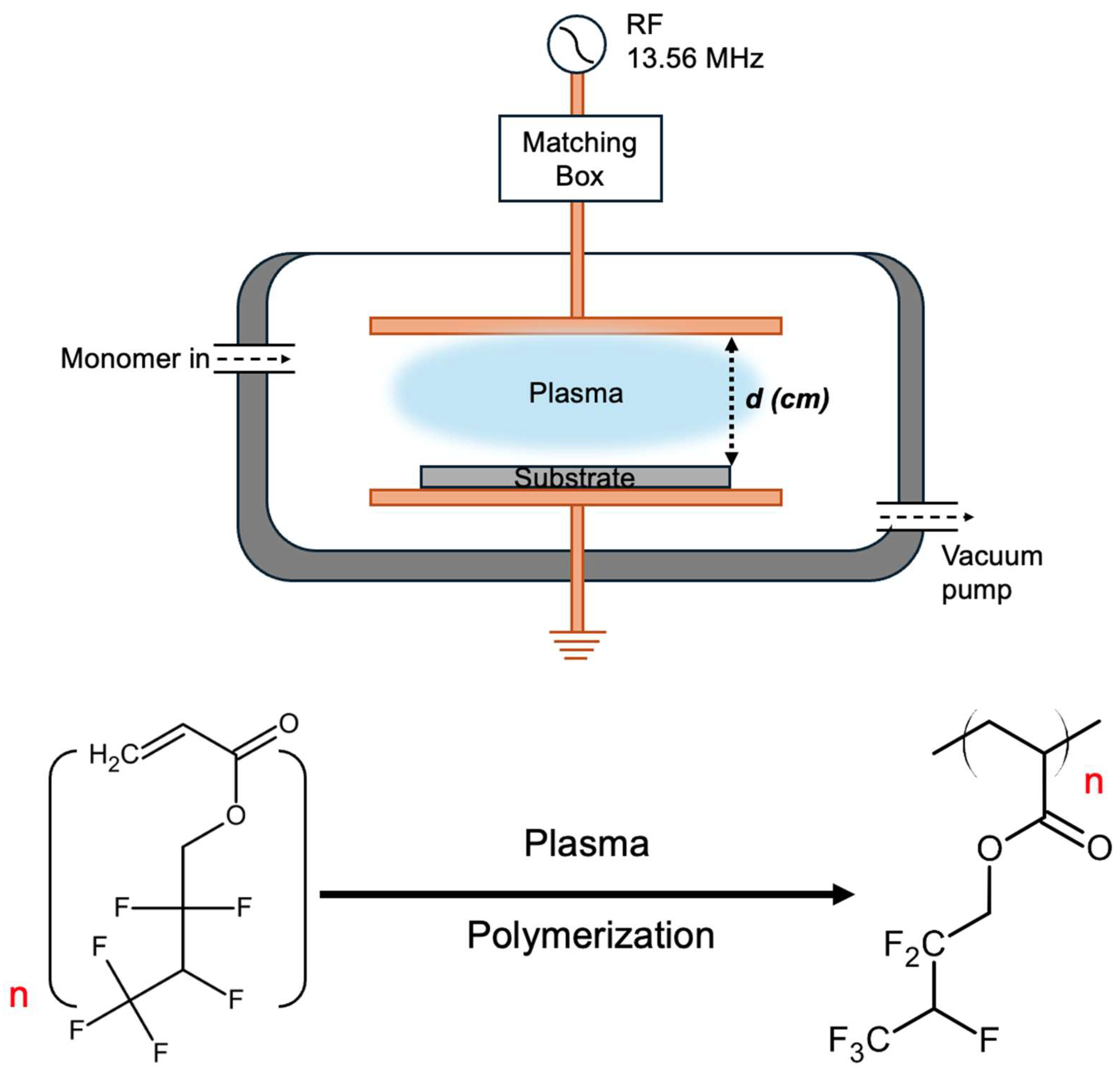
2.2. Method
2.3. Characterizations
3. Results and Discussion
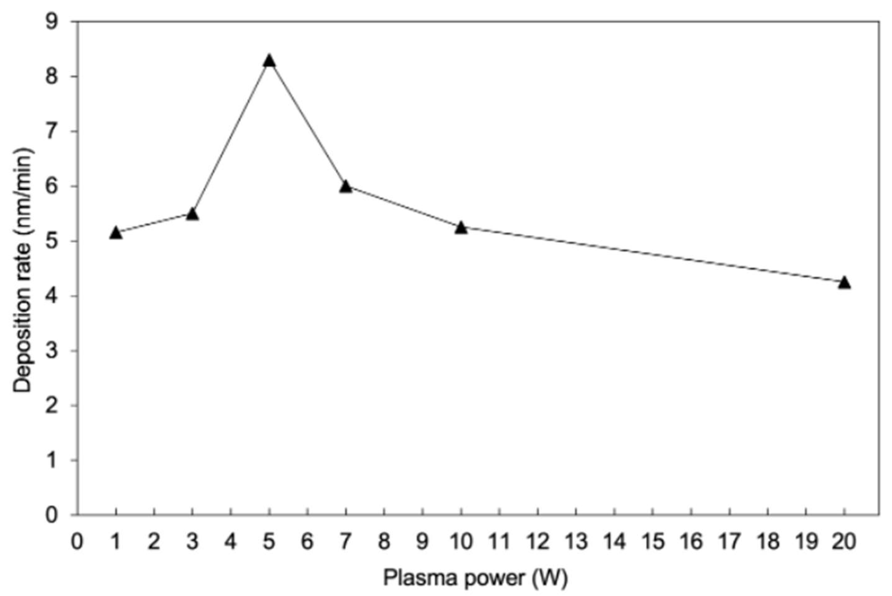
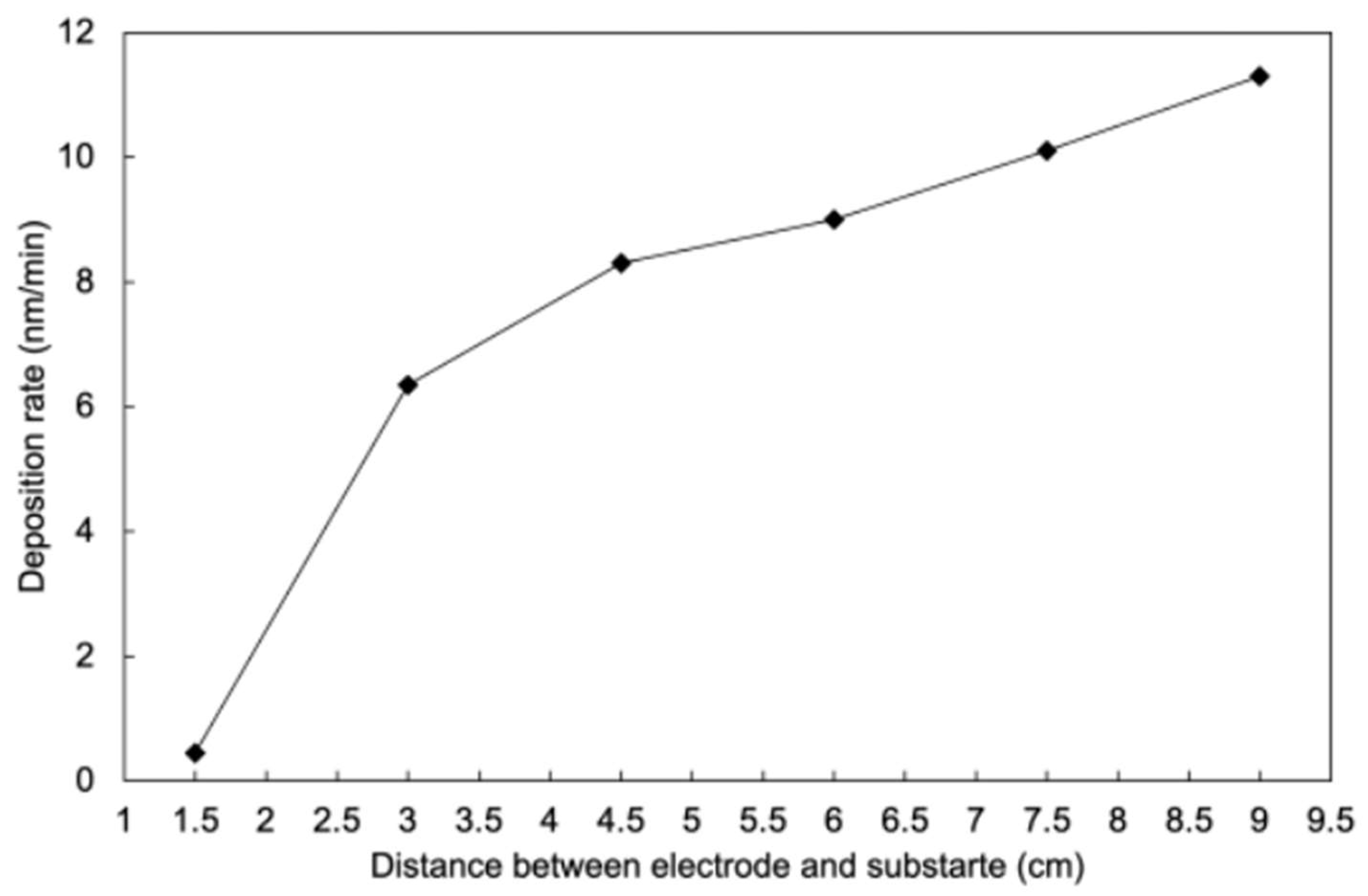
3.1. Deposition Rates
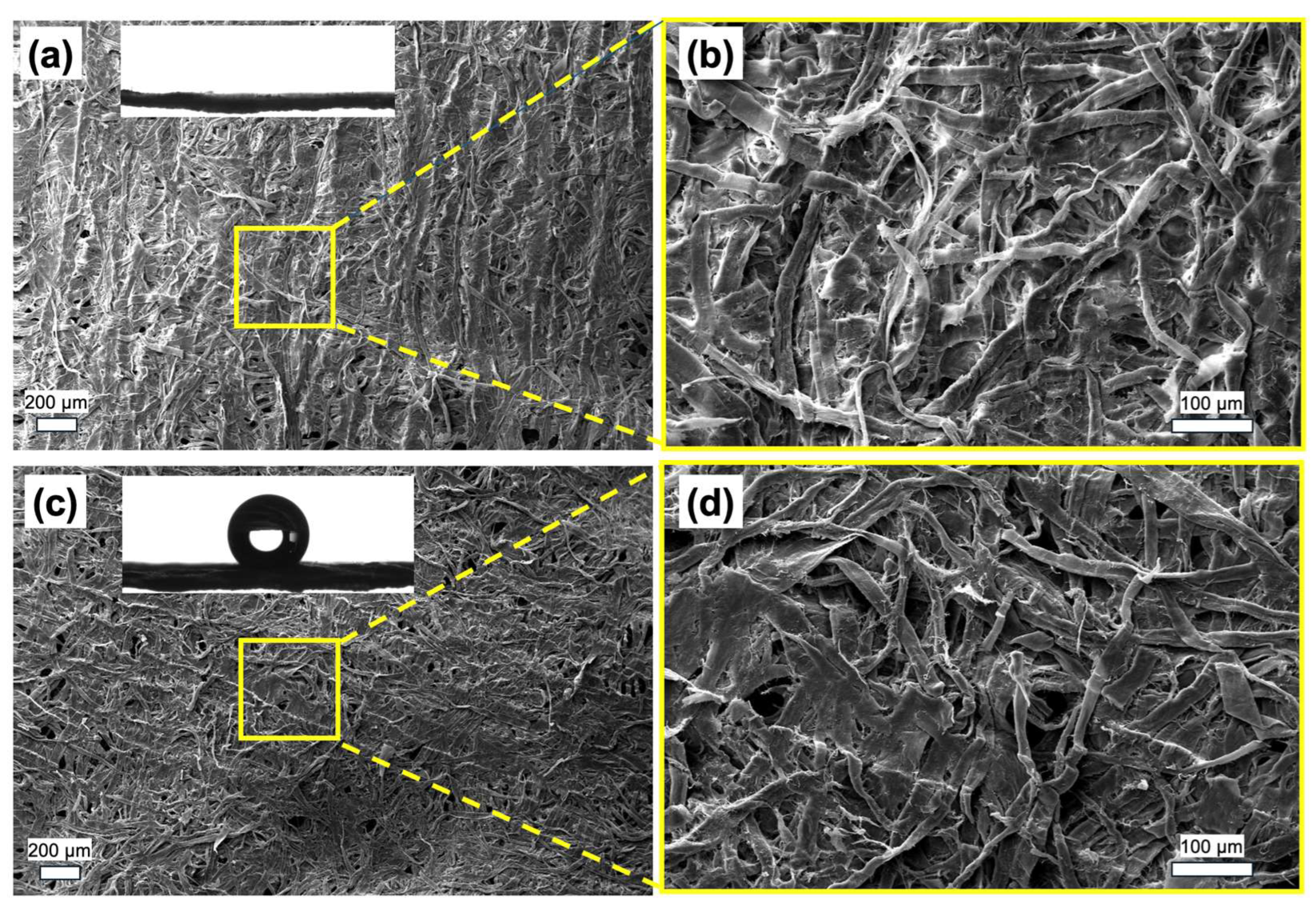
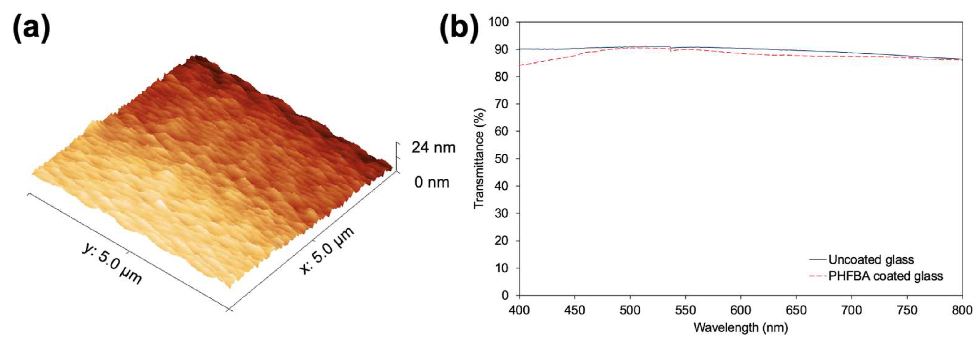
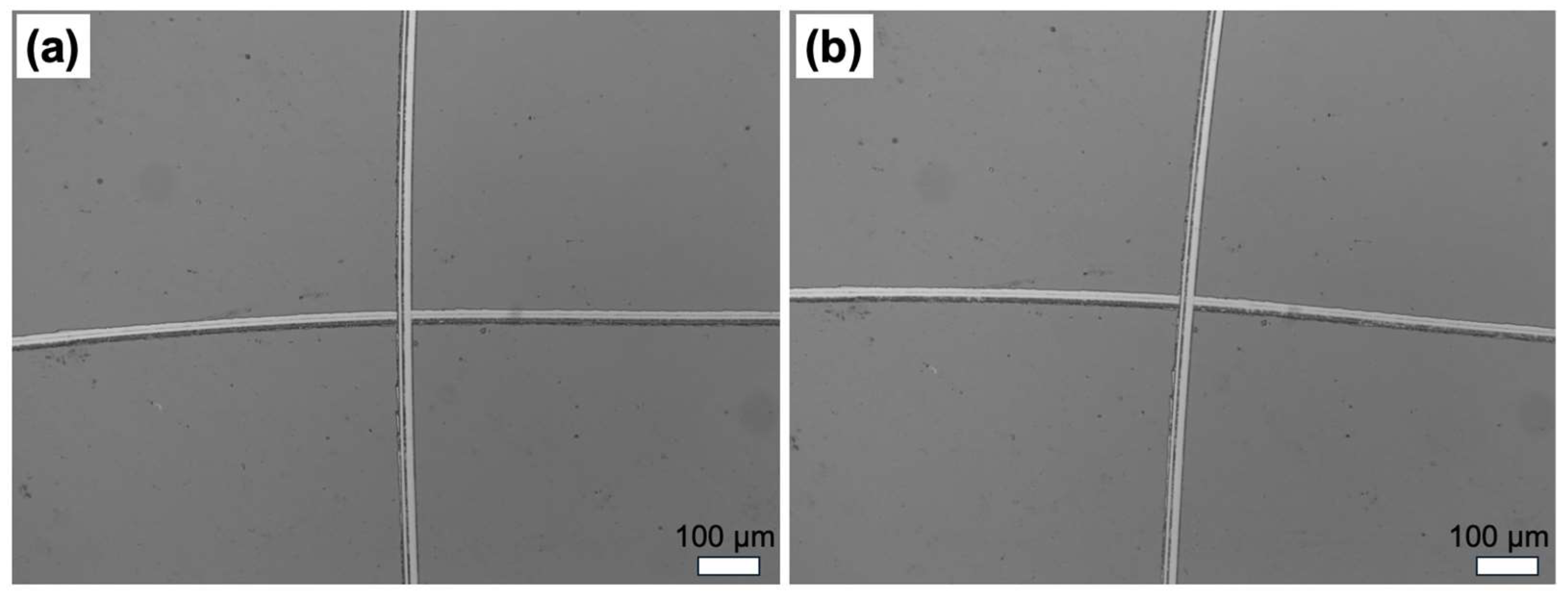
3.2. Film Structure
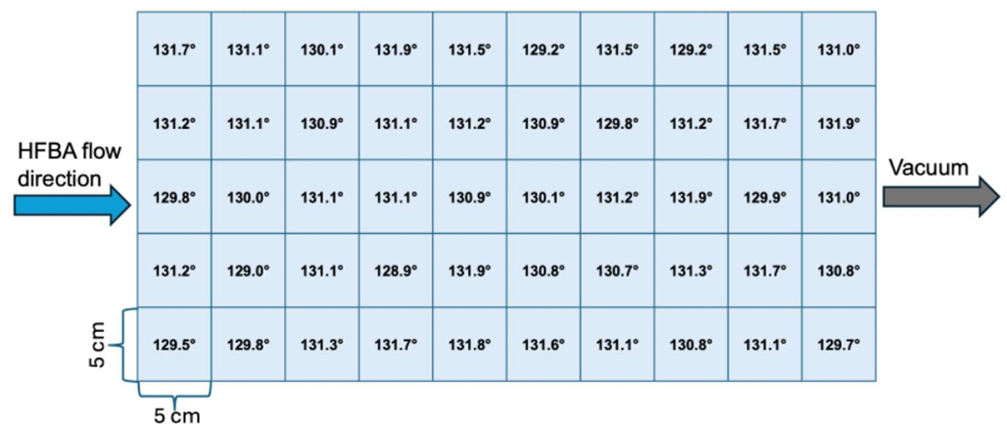
3.3. Large-Scale Depostion
4. Conclusions
Author Contributions
Funding
Institutional Review Board Statement
Data Availability Statement
Conflicts of Interest
References
- Hu, X.; Wei, X.; Naik, A.R.; Bradley, L.C.; Watkins, J.J. Rapid scalable fabrication of stable copper electrowetting valves. Microfluid. Nanofluid. 2023, 27, 63. [Google Scholar] [CrossRef]
- Samadi, A.; Ni, T.; Fontananova, E.; Tang, G.; Shon, H.; Zhao, S. Engineering antiwetting hydrophobic surfaces for membrane distillation: A review. Desalination 2023, 563, 116722. [Google Scholar] [CrossRef]
- Pawelec, K.M.; Tu, E.; Chakravarty, S.; Hix, J.M.; Buchanan, L.; Kenney, L.; Buchanan, F.; Chatterjee, N.; Das, S.; Alessio, A. Incorporating tantalum oxide nanoparticles into implantable polymeric biomedical devices for radiological monitoring. Adv. Healthc. Mater. 2023, 12, 2203167. [Google Scholar] [CrossRef]
- Chaudhuri, A.; Maity, J. Durable hydrophobic polymer coating on silk surface by surfactant-aided fluoro-monomer polymerization through admicellar technique. Mater. Today Proc. 2023, 73, 567–575. [Google Scholar] [CrossRef]
- Liang, T.; Neumann, C.N.; Ritter, T. Introduction of fluorine and fluorine-containing functional groups. Angew. Chem. Int. Ed. 2013, 52, 8214–8264. [Google Scholar] [CrossRef]
- Grandjean, P.; Clapp, R. Changing interpretation of human health risks from perfluorinated compounds. Public Health Rep. 2014, 129, 482–485. [Google Scholar] [CrossRef]
- Lau, C.; Anitole, K.; Hodes, C.; Lai, D.; Pfahles-Hutchens, A.; Seed, J. Perfluoroalkyl acids: A review of monitoring and toxicological findings. Toxicol. Sci. 2007, 99, 366–394. [Google Scholar] [CrossRef]
- Olsen, G.W.; Chang, S.-C.; Noker, P.E.; Gorman, G.S.; Ehresman, D.J.; Lieder, P.H.; Butenhoff, J.L. A comparison of the pharmacokinetics of perfluorobutanesulfonate (PFBS) in rats, monkeys, and humans. Toxicology 2009, 256, 65–74. [Google Scholar] [CrossRef]
- Yu, Z.; Wu, S.; Li, C.; Xiao, Y.; Zheng, L.; Liu, J.; Zhang, B. Ultra-low dielectric constant fluorinated graphene/polybenzoxazole composite films with excellent thermal stabilities and mechanical properties. Compos. Part A Appl. Sci. Manuf. 2021, 145, 106387. [Google Scholar] [CrossRef]
- Jung, H.; Kwon, J.; Jung, H.; Cho, K.M.; Yu, S.J.; Lee, S.M.; Jeon, M.; Im, S.G. Short-chain fluorocarbon-based polymeric coating with excellent nonwetting ability against chemical warfare agents. RSC Adv. 2022, 12, 7773–7779. [Google Scholar] [CrossRef]
- Gürsoy, M.; Karaman, M. Hydrophobic coating of expanded perlite particles by plasma polymerization. Chem. Eng. J. 2016, 284, 343–350. [Google Scholar] [CrossRef]
- Şakalak, H.; Yılmaz, K.; Gürsoy, M.; Karaman, M. Roll-to roll initiated chemical vapor deposition of super hydrophobic thin films on large-scale flexible substrates. Chem. Eng. Sci. 2020, 215, 115466. [Google Scholar] [CrossRef]
- Karaman, M.; Gürsoy, M.; Aykül, F.; Tosun, Z.; Kars, M.D.; Yildiz, H.B. Hydrophobic coating of surfaces by plasma polymerization in an RF plasma reactor with an outer planar electrode: Synthesis, characterization and biocompatibility. Plasma Sci. Technol. 2017, 19, 085503. [Google Scholar] [CrossRef]
- Lin, J.; Zheng, C.; Ye, W.; Wang, H.; Feng, D.; Li, Q.; Huan, B. A facile dip-coating approach to prepare SiO2/fluoropolymer coating for superhydrophobic and superoleophobic fabrics with self-cleaning property. J. Appl. Polym. Sci. 2015, 132, 41458. [Google Scholar] [CrossRef]
- Lock Sulen, W.; Ravi, K.; Bernard, C.; Ichikawa, Y.; Ogawa, K. Deposition mechanism analysis of cold-sprayed fluoropolymer coatings and its wettability evaluation. J. Therm. Spray Technol. 2020, 29, 1643–1659. [Google Scholar] [CrossRef]
- Shi, C.; Wang, J.; Zhou, Y.; Lu, X.; Chang, G.; Pan, A.; He, L. Fabrication of POSS-tethered fluorinated glycidyl copolymers as durable hydrophobic and adhesive coatings. Prog. Org. Coat. 2024, 193, 108535. [Google Scholar] [CrossRef]
- Zhang, Z.; Chen, K.; Ameduri, B.; Chen, M. Fluoropolymer nanoparticles synthesized via reversible-deactivation radical polymerizations and their applications. Chem. Rev. 2023, 123, 12431–12470. [Google Scholar] [CrossRef]
- Grigoreva, A.; Vihireva, A.; Zaitsev, S. Synthesis of functional fluorinated copolymers with different microstructure via reversible addition-fragmentation chain transfer (RAFT) process. Polym. Bull. 2024, 81, 8701–8722. [Google Scholar] [CrossRef]
- Franz, G. Plasma enhanced chemical vapor deposition of organic polymers. Processes 2021, 9, 980. [Google Scholar] [CrossRef]
- Gürsoy, M. Fabrication of poly (N-isopropylacrylamide) with higher deposition rate and easier phase transition by initiated plasma enhanced chemical vapor deposition. Plasma Chem. Plasma Process. 2020, 40, 1063–1079. [Google Scholar] [CrossRef]
- Şakalak, H.; Yilmaz, K.; Gürsoy, M.; Karaman, M. Roll-to-Roll Vapor Deposition of Hydrophobic and Transparent Nano-Adhesive Polymeric Thin Films on Rigid and Flexible Substrates. Ind. Eng. Chem. Res. 2022, 61, 8839–8846. [Google Scholar] [CrossRef]
- Gürsoy, M. Fabrication of paper-based microfluidic devices using PECVD for selective separation. Macromol. Res. 2021, 29, 423–429. [Google Scholar] [CrossRef]
- Chakounté, R.M.; Jolibois, J.; Kappertz, O.; Chambers, J.; Weis, H.; Wiame, H.; Viöl, W. Water and oil repellent coating on fabric using hollow cathode PECVD. Surf. Coat. Technol. 2022, 446, 128816. [Google Scholar]
- Cheng, C.; Gupta, M. Roll-to-Roll Surface Modification of Cellulose Paper via Initiated Chemical Vapor Deposition. Ind. Eng. Chem. Res. 2018, 57, 11675–11680. [Google Scholar] [CrossRef]
- Karaman, M.; Cam, S.M.; Çelen, O.; Özbakış, M.; Yılmaz, K. Reel-to-Reel Coating of a Conductive Polymer on Synthetic Textile Yarns in a Semi-closed Batch Oxidative CVD System. Fibers Polym. 2024, 25, 2597–2603. [Google Scholar] [CrossRef]
- Gürsoy, M.; Uçar, T.; Tosun, Z.; Karaman, M. Initiation of 2-Hydroxyethyl Methacrylate Polymerization by Tert-Butyl Peroxide in a Planar PECVD System. Plasma Process. Polym. 2016, 13, 438–446. [Google Scholar] [CrossRef]
- Hegemann, D.; Hossain, M.M.; Körner, E.; Balazs, D.J. Macroscopic Description of Plasma Polymerization. Plasma Process. Polym. 2007, 4, 229–238. [Google Scholar] [CrossRef]
- de los Arcos, T.; Awakowicz, P.; Benedikt, J.; Biskup, B.; Böke, M.; Boysen, N.; Buschhaus, R.; Dahlmann, R.; Devi, A.; Gergs, T.; et al. PECVD and PEALD on polymer substrates (part I): Fundamentals and analysis of plasma activation and thin film growth. Plasma Process. Polym. 2024, 21, 2300150. [Google Scholar] [CrossRef]
- Morosoff, N. 1—An Introduction to Plasma Polymerization. In Plasma Deposition, Treatment, and Etching of Polymers; d’Agostino, R., Ed.; Academic Press: San Diego, CA, USA, 1990; pp. 1–93. [Google Scholar]
- Petruczok, C.D.; Chen, N.; Gleason, K.K. Closed batch initiated chemical vapor deposition of ultrathin, functional, and conformal polymer films. Langmuir 2014, 30, 4830–4837. [Google Scholar] [CrossRef]
- Smith, P.M.; Su, L.; Xu, Y.; Reeja-Jayan, B.; Shen, S. Morphological and molecular control of chemical vapor deposition (CVD) polymerized polythiophene thin films. RSC Adv. 2024, 14, 31723–31729. [Google Scholar] [CrossRef]
- Genna, S.; Leone, C.; Moretti, P.; Venettacci, S. Influence of Polymer Surface Roughness on the Fractions of Transmitted, Reflected and Absorbed Energy in Operation of Laser Transmission Welding. Lasers Manuf. Mater. Process. 2024, 11, 469–491. [Google Scholar] [CrossRef]
- Larena, A.; Millán, F.; Pérez, G.; Pinto, G. Effect of surface roughness on the optical properties of multilayer polymer films. Appl. Surf. Sci. 2002, 187, 339–346. [Google Scholar] [CrossRef]
- Manifacier, J.; Gasiot, J.; Fillard, J.P. A simple method for the determination of the optical constants n, k and the thickness of a weakly absorbing thin film. J. Phys. E Sci. Instrum. 1976, 9, 1002. [Google Scholar] [CrossRef]
- Zhang, Y.; Yan, Y.; Wang, Y.; Li, Y.; Wang, X.; Zhang, H.; Liu, J.; Wang, F. The synthesis and solution properties of hyperbranched polyglycerols modified with hexafluorobutyl acrylate. Colloids Surf. A Physicochem. Eng. Asp. 2013, 436, 563–569. [Google Scholar] [CrossRef]
- Lin-Vien, D.; Colthup, N.B.; Fateley, W.G.; Grasselli, J.G. The Handbook of Infrared and Raman Characteristic Frequencies of Organic Molecules; Elsevier: Amsterdam, The Netherlands, 1991. [Google Scholar]
- Beamson, G. High Relution XPS of Organic Polymers. The Scienta ESCA 300 Database; ICIplc: London, UK, 1992. [Google Scholar]
- Gupta, M.; Gleason, K.K. Initiated Chemical Vapor Deposition of Poly(1H,1H,2H,2H-perfluorodecyl Acrylate) Thin Films. Langmuir 2006, 22, 10047–10052. [Google Scholar] [CrossRef]
- Badyal, J.P. Beyond the surface-Cold plasmas are streamlining the surface coatings industry. Chem. Br. 2001, 37, 45–46. [Google Scholar]
- Rupper, P.; Vandenbossche, M.; Bernard, L.; Hegemann, D.; Heuberger, M. Composition and stability of plasma polymer films exhibiting vertical chemical gradients. Langmuir 2017, 33, 2340–2352. [Google Scholar] [CrossRef]
- Vasudev, M.C.; Anderson, K.D.; Bunning, T.J.; Tsukruk, V.V.; Naik, R.R. Exploration of plasma-enhanced chemical vapor deposition as a method for thin-film fabrication with biological applications. ACS Appl. Mater. Interfaces 2013, 5, 3983–3994. [Google Scholar] [CrossRef]
- Pfluger, C.A.; Carrier, R.L.; Sun, B.; Ziemer, K.S.; Burkey, D.D. Cross-linking and degradation properties of plasma enhanced chemical vapor deposited poly (2-hydroxyethyl methacrylate). Macromol. Rapid Commun. 2009, 30, 126–132. [Google Scholar] [CrossRef]
- Gorga, R.E.; Lau, K.K.; Gleason, K.K.; Cohen, R.E. The importance of interfacial design at the carbon nanotube/polymer composite interface. J. Appl. Polym. Sci. 2006, 102, 1413–1418. [Google Scholar] [CrossRef]


| C1s | Origin | Binding Energy (eV) Theoretical | Binding Energy (eV) Experimental |
|---|---|---|---|
| 1 | C-C*H2-C | 285.0 | 285.1 |
| 2 | C*H-CO | 285.7 | 285.6 |
| 3 | O-C*H2 | 286.7 | 286.2 |
| 4 | CH2-CF2-C*HF | 286.8 | 287.3 |
| 5 | C*=O | 289.2 | 289.2 |
| 6 | C*F2 | 291.2 | 290.8 |
| 7 | C*F3 | 293.3 | 293.6 |
Disclaimer/Publisher’s Note: The statements, opinions and data contained in all publications are solely those of the individual author(s) and contributor(s) and not of MDPI and/or the editor(s). MDPI and/or the editor(s) disclaim responsibility for any injury to people or property resulting from any ideas, methods, instructions or products referred to in the content. |
© 2025 by the authors. Licensee MDPI, Basel, Switzerland. This article is an open access article distributed under the terms and conditions of the Creative Commons Attribution (CC BY) license (https://creativecommons.org/licenses/by/4.0/).
Share and Cite
Yılmaz, K.; Gürsoy, M.; Karaman, M. Large-Area Deposition of Hydrophobic Poly(hexafluorobutyl Acrylate) Thin Films on Wetting-Sensitive and Flexible Substrates via Plasma-Enhanced Chemical Vapor Deposition. Polymers 2025, 17, 791. https://doi.org/10.3390/polym17060791
Yılmaz K, Gürsoy M, Karaman M. Large-Area Deposition of Hydrophobic Poly(hexafluorobutyl Acrylate) Thin Films on Wetting-Sensitive and Flexible Substrates via Plasma-Enhanced Chemical Vapor Deposition. Polymers. 2025; 17(6):791. https://doi.org/10.3390/polym17060791
Chicago/Turabian StyleYılmaz, Kurtuluş, Mehmet Gürsoy, and Mustafa Karaman. 2025. "Large-Area Deposition of Hydrophobic Poly(hexafluorobutyl Acrylate) Thin Films on Wetting-Sensitive and Flexible Substrates via Plasma-Enhanced Chemical Vapor Deposition" Polymers 17, no. 6: 791. https://doi.org/10.3390/polym17060791
APA StyleYılmaz, K., Gürsoy, M., & Karaman, M. (2025). Large-Area Deposition of Hydrophobic Poly(hexafluorobutyl Acrylate) Thin Films on Wetting-Sensitive and Flexible Substrates via Plasma-Enhanced Chemical Vapor Deposition. Polymers, 17(6), 791. https://doi.org/10.3390/polym17060791