Article

Large Stepwise Discrete Microsystem Displacements Based on Electrostatic Bending Plate Actuation

Microsystems Technology (MST), Faculty of Electrical Engineering and Information Technology, Ruhr-University Bochum (RUB), 44801 Bochum, Germany
*
Authors to whom correspondence should be addressed.
Actuators 2021, 10(10), 272; https://doi.org/10.3390/act10100272
Submission received: 9 September 2021 / Revised: 8 October 2021 / Accepted: 12 October 2021 / Published: 15 October 2021
(This article belongs to the Special Issue Cooperative Microactuator Systems)

Abstract

:
We present the design, fabrication, and experimental characterization of microsystems achieving large and stepwise discrete displacements. The systems consist of electrostatic bending plate actuators linked in a chain with increasing electrode gaps to allow a stepwise system displacement. A derived analytic transfer function permits to evaluate the influence of the system components on both the total and the stepwise system displacement. Based on calculation and simulation results, systems featuring 5, 8, 10, 13, and 16 steps are modeled and fabricated using a dicing-free SOI-fabrication process. During experimental voltage- and time-dependent system characterization, the minimum switching speed of the electrostatic actuators is 1 ms. Based on the guiding spring stiffness and the switching time, step-by-step and collective activations of the microsystems are performed and the system properties are derived. Furthermore, we analyze the influence of the number of steps on the total system displacement and present 16-step systems with a total maximum displacement of 230.7 ± 0.9 µm at 54 V.

1. Introduction

The presented multistage and multistable actuator system with a large stroke was motivated by terahertz (THz) applications. For THz systems, a true time delay is required, usually subdivided in binary fractions of the wavelength [1]. To achieve such a true time delay of THz beam steering arrays, a stepwise high-throw actuator microelectromechanical system (MEMS) would be a perfect solution.
Due to the fast response to electric signals [2] and the suitability for harsh environments [3,4], electrostatic actuators are used in THz systems [5] for optical switching [6], capacitors [7], micromirrors [8], and biomedical applications [9]. The usage in underwater environments [3] and in wearable haptics [10] enlarges the application field and increases the demand for large displacement and quick response electrostatic actuators.
Electrostatic actuators appear in many different varieties, of which the comb-drive and the parallel-plate actuators are the best known. Legtenberg et al. [11], amongst others, were pioneers showing the importance of the guiding springs enlarging the displacement of the comb-drives. By adapting the shuttle geometry, Grade et al. [2] demonstrated that these actuators can achieve displacements up to 150 µm in less than 1 ms with operating voltages below 150 V.
Electrostatic parallel-plate actuators reduce the distance between the electrodes in response to an applied voltage [12]. Various investigations [13,14,15,16,17] to reach a stable and large displacement by controller architectures resulted in a high input voltage and a sensitivity to parasitic capacitance. Thus, by adding an isolating layer between the electrodes and by adapting the electrode design, large and stable displacements can be achieved. Based on this, in [6], deflections exceeding 62.5 µm are reported at a driving voltage below 30 V. Therefore, a very long flexible electrode was combined with a rigid cantilever. Preetham et al. [3] report a peak-to-peak displacement of 19.5 µm at ±8 V using curved isolated electrodes. In [18], we present a 3-bit digital-to-analog converter achieving a displacement of 149.5 µm at 60 V. In [19], we present three bending plate actuators linked in a chain and achieving a stepwise displacement of up to 35.8 µm at 50 V.
In this contribution, we present microsystems consisting of numerous flexible electrostatic bending plate actuators linked in a chain and achieving large displacements of up to 230.7 ± 0.9 µm at 54 V. In Section 2, we present the system function and derive the analytical transfer function to model microsystems with multiple steps. We focus on the sinusoidal guiding springs [20] and their huge influence on the system displacement. In Section 3, we show the fabrication of the systems featuring 5, 8, 10, 13, and 16 steps which are based on a dicing-free SOI-technology [21,22,23]. In Section 4, we characterize the bending plate actuators with a focus on the influence of the electrode geometry. Then, step-by-step and collective actuator activations as well as the switching time are presented. Finally, the system behavior depending on the number of steps and the guiding spring is analyzed. The main achievements of this work are summarized in Section 5.

2. Concept

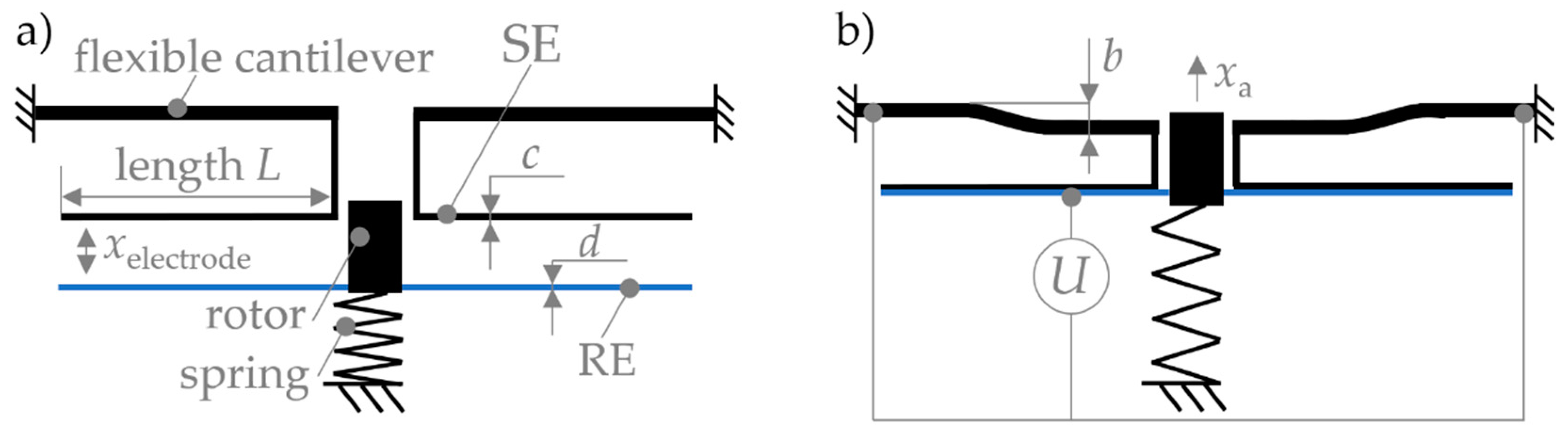
2.1. Flexible Electrostatic Bending Plate Actuators

The required displacement of about 20 μm is generated by flexible electrostatic bending plate actuators. These actuators are based on a rotor electrode (RE) and a stator electrode (SE) facing each other at the distance xelectrode (Figure 1a). The rotor electrode is fixed to a spring-mounted rotor. The stator electrode is combined with a flexible cantilever. When a voltage is applied between the electrodes, the tips of the electrodes approach as soon as the electrostatic force between the electrodes exceeds the overall mechanical force of springs and electrodes. Therefore, the electrodes bend towards each other which is the origin to name these actuators bending plate actuators. The bending of the electrodes starts with the tips approaching each other as the electrodes feature the smallest stiffness at the tips. This behavior is examined experimentally in Section 4.2.2. With increasing voltage, the cantilever of the stator electrode bends down the distance b. The pull-in is completed as soon as the electrodes are completely in contact, as shown in Figure 1b.
The bending of the flexible cantilever reduces the maximum displacement of the actuator xa. Thus, the flexibility of the cantilever reduces the pull-in voltage of the actuator as the stiffness of the electrodes increases with increasing distance to the tips. Therefore, the cantilever bending is a compromise between a reduction of the pull-in voltage and a reduction of the maximum displacement. In [19] we show that the maximum displacement range of the actuator xa is the electrode gap xelectrode considering the bending b of the cantilever, which yields:
x a = x electrode b

2.2. System Function

The cooperative system setup is shown in Figure 2a [19]. The system consists of multiple electrostatic bending plate actuators (a1, a2, …, aj) linked in a chain by connecting springs (k1, k2, …, kj) with the identical stiffness k. The first actuator a1 has the smallest initial electrode gap x1. With each actuator, the initial gap increases, so the last actuator aj has the largest initial electrode gap xj. A main sinusoidal guiding spring kg [20] is directly connected to the last actuator and guarantees a pure translational system displacement xsystem,i. The connecting spring k1 and the guiding spring kg are coupled to the substrate of the chip.
When activating the first actuator a1, this actuator displaces and its displacement is conducted through the system generating a system displacement xsystem,1. The displacement of the system xsystem,i when activating actuator ai is always identical to the reduction of xj of the last actuator aj (for ij) minus the deformation of the connecting springs. Therefore, considering the bending of the cantilever (Equation (1)), the maximum total system displacement xsystem,j is the electrode gap distance xj minus the bending of the cantilever bj.

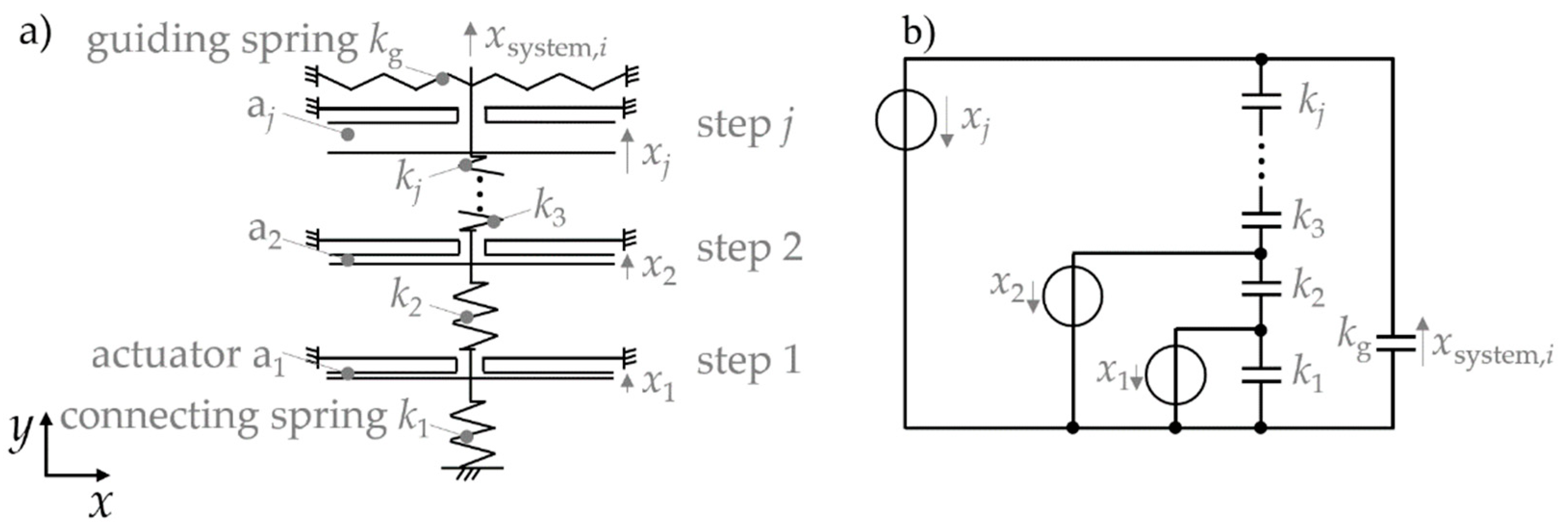
2.3. Step-by-Step and Collective Actuation

When the system is actuated step-by-step, an actuator can only be activated if all actuators with smaller electrode gaps are already completely pulled-in. The step-by-step actuation can be described analytically based on an associated analogous electrical network model (Figure 2b). In the network model, the actuators are associated with potential sources and the mechanical springs are modeled as capacitors.
When actuator a1 is activated, it travels the distance x1 and the system travels the range xsystem,1. When the actuators a1 and a2 are activated, the system travels the range xsystem,2. By successively activating the individual electrostatic actuators, a stepwise system displacement is generated. Therefore, xsystem,j represents the displacement of the system composed of j actuators when all actuators are displaced and, e.g., xsystem,3 represents the displacement of a system composed of j actuators when the actuators a1, a2 and a3 are displaced (for 3 ≤ j). The system displacement xsystem,i when activating i actuators in a system consisting of j actuators (ij) is described by Equation (2):
x s y s t e m , i = x i k g · ( j i k i + 1 k g )                               ,   f o r   i   j
When applying a voltage to the first actuator a1, this actuator generates a displacement x1 that is conducted through the entire system. This initial displacement reduces the gaps between the electrodes of all following actuators a2 to aj. For a structure composed of j actuators, Equation (3) describes the displacement xi of actuator ai when actuating all actuators with a smaller electrode gap distance (a1, a2, …, ai1):
x a , i = m = 2 i x system , m 1 · k g · ( j i k i + 1 k g )   ,   f o r   2 i   j
Based on Equations (2) and (3), a higher stiffness of the guiding spring kg reduces the system displacement, whereas a higher stiffness of the connecting springs (k1, …, kj) increases the displacement.
For the step-by-step actuation, each actuator requires its own wiring and bond pad (BP) making the control circuitry complex and enlarging the system’s footprint. In Figure 3a 5-step system is shown. Equation (4) describes the relation between the number of steps i and the number of bond pads p:
p = 2 · i + 1
During a collective actuation all electrostatic actuators are actuated at the same time so that a single wiring is required on each side, only. The collective actuation is suitable for systems with a large stroke realized by multiple steps, such as the 16-step system shown in Figure 3b. The displacement during collective actuation depends on the applied voltage. Systems with a step-by-step setup can also be actuated collectively, whereas systems with a collective setup cannot be actuated step-by-step.

2.4. System Setup Based on Modelling and Simulation

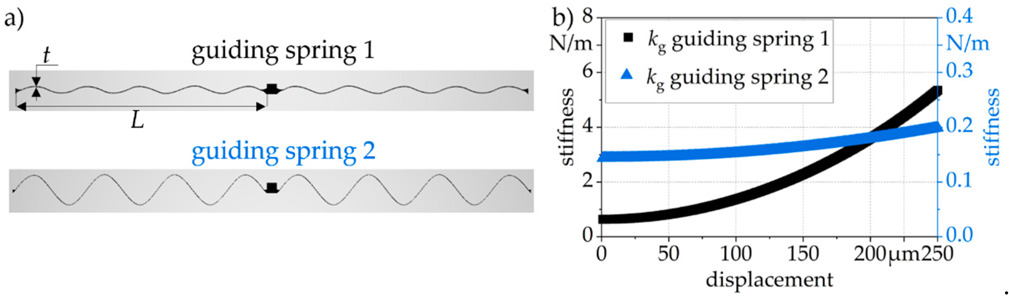
2.4.1. System Design Based on the Guiding Spring

Sinusoidal guiding springs [20] as shown in Figure 4a are well-suited for the stepwise systems as they feature a very low stiffness in deflection direction lowering the pull-in voltage. However, in wafer plane off-axis direction the high stiffness of these springs ensures a purely translational guiding of the system. Thereby, the selectivity of the sinusoidal spring decreases with an increasing amplitude of the sinusoids [20].
To analyse the influence of the guiding spring on the system function, two different sinusoidal guiding springs are used. Guiding spring 1 features 4.5 sinusoids with an amplitude of 26.8 µm. The length L is 2425 µm, the thickness t amounts to 8 µm, and the width w to 50 µm. Guiding spring 2 has 3.5 sinusoids with an amplitude of 142.25 µm. The length L amounts to 2450 µm, the thickness t is 5 µm, and the width w is 50 µm. The fabricated guiding springs are shown in Figure 15 and the fabricated guiding spring 2 is additionally shown in Figure 3.
Based on COMSOL Multiphysics solid state simulation, the stiffness of guiding spring 1 increases strongly, whereas guiding spring 2 shows a lower and more constant spring stiffness (Figure 4b).
Two system design options can be selected: a design considering a mean stiffness value of the guiding spring and a design considering the actual stiffness value of the guiding spring as a function of displacement.
For both design options, 16-step systems guided by the mentioned guiding spring 1 (Figure 5a) or guiding spring 2 (Figure 5b), respectively, are designed based on Equation (2) to determine the system displacement xsystem,i and on Equation (3) to determine the electrode gaps xi. The mean and actual stiffness of the guiding springs are determined based on the COMSOL Multiphysics simulation results presented in Figure 4b.
The step-by-step actuation follows the idea to use the same voltage for the actuation of each single step. The use of the same voltage for each step simplifies the automated electrical control of the actuators with a single voltage source. To ensure that each actuator requires the same voltage, based on Equations (2) and (3), the electrode gap is calculated with the aim to always have the same distance when actuating the actuator. For the calculation an electrode distance of 20 µm is used. Therefore, e.g., for system 1: when no actuator is actuated, actuator a1 has an electrode gap of 20 µm and actuator a2 of 38.28 µm. When actuating a1, actuator a1 will pull in and based on Equation (3) the actuator a2 will travel the distance 18.28 µm, so that now the actuator a2 has an electrode gap of 20 µm. For this setup, we assume that an equal electrode gap results in an equal voltage for complete pull-in and we neglect the cantilever bending.
For steps 1 to 15, the electrode gaps exceed the system displacement as the actuator displacement partly results in a deformation of the connecting springs. Comparing Figure 5a,b the guiding spring design highly influences the system. As the stiffness of guiding spring 2 is almost constant in the required deflection range (Figure 4b), the mean stiffness value and the actual stiffness value systems do not differ much (Figure 5b). Due to the high increase in the stiffness of guiding spring 1, the mean stiffness deviates from the actual spring stiffness so that the actual stiffness value system differs from the mean stiffness value system in Figure 5a. The decrease in the electrode gap as marked in Figure 5a is due to the high stiffness of guiding spring 1 counteracting the system displacement by deforming the connecting springs.
The systems in Figure 5a,b only differ in the guiding spring. Consequently, the guiding spring has a high influence on the resulting system displacement. For both systems, the system displacement is shown based on the actual and on the mean guiding spring stiffness. For the system guided by the low-stiffness spring 2 (Figure 5b), the system displacement does not differ much concerning the actual and the mean stiffness. Thus, the analytical system design is much more complex when calculating with the actual spring stiffness. Therefore, when using a low-stiffness guiding spring, the use of a mean stiffness of the guiding spring can decrease the design effort without a notable influence on the resulting system displacement. For a high-stiffness guiding spring (Figure 5a), it is useful to design the system with the actual spring stiffness to enlarge the resulting system displacement.

2.4.2. System Design for Different Step Numbers

Figure 6 shows electrode gaps of systems featuring a mean stiffness design depending on the number of steps. Based on the idea of equal pull-in voltages as explained in paragraph 2.4.1, the electrode gaps are designed calculating with an electrode gap of 20 µm. Therefore, Equations (2) and (3) are used.
For the systems in Figure 6a featuring the high stiffness guiding spring 1, the electrode gaps depend on the number of steps in the system. Due to the system setup, the maximum system displacement xsystem,j is equal to the electrode gap of the last actuator aj minus the bending bj of the cantilever. Assuming a negligible small cantilever bending, the calculated total displacements of, the 5-, 8-, 10-, 13-, and 16-step systems amount to 54.7 µm, 67.9 µm, 74.5 µm, 82.5 µm and 88.9 µm, respectively. Consequently, the average step size decreases with an increasing number of steps. The reason is found in the increasing number of connecting springs that deform and therefore reduce the displacement that can be conducted to the following actuators. This deformation of the connecting springs is increased due to the high stiffness of guiding spring 1.
Guiding spring 2 (Figure 6b) features a lower stiffness, and therefore the electrode gaps do not differ much for the systems featuring the low stiffness guiding spring 2. The 5-step system achieves a maximum displacement of 91.9 µm, the 8-, 10-, 13-, and 16-step systems of 139.0 µm, 167.7 µm, 207.5 µm and 244.0 µm, respectively.

2.4.3. Overview of the Modelled Systems

Based on the discussion in paragraph 2.4.1, the systems featuring the low-stiffness guiding spring 2 are modeled with a mean stiffness value (system 3 to 6) and the system featuring the high-stiffness guiding spring 1 with the actual stiffness value (system 7). The only exception are the 5-step systems as the influence of the guiding spring is smaller for a smaller number of steps (paragraph 2.4.2, Figure 6a).
The modeled microsystems are shown in Table 1. All systems feature connecting springs with a stiffness ki = 4.9 N/m at 20 µm displacement. The fabricated connecting springs are shown in Figure 3. They feature a length of 1965 µm, a thickness of 12 µm, a width of 50 µm and 1.5 sinusoids with an amplitude of 47.5 µm. The systems have 5, 8, 10, 13 and 16 steps. The 5-step systems can be activated step-by-step and collectively. Due to the high number of bond pads, systems with more than 5 steps can only be activated collectively.

3. Fabrication

The microsystems are fabricated on (100)-oriented silicon-on-insulator (SOI) wafers with a 300 µm thick handle layer and a 50 µm device layer.
A 100 nm aluminum layer is deposited on the device layer by evaporation, and the bond pads are patterned by wet chemical etching (Figure 7a). To minimize the risk of a pull-in between the electrostatic actuators and the handle layer during electronic activation, the chips make use of a dicing-free process [21,22,23] removing the handle layer from the backside of the electrostatic actuators during hydrofluoric (HF) acid vapor etching. This process also separates the single chips from each other, making a mechanical sawing process obsolete. Therefore, the handle layer is deep etched (DRIE, Figure 7b). A 400 nm plasma-deposited SiO2 layer (Figure 7c) is used as a hard mask for the patterning of the systems. Then, also the device layer is deep etched (Figure 7d). The systems are released by HF-vapor etching (Figure 7e). The electrical isolation of the electrodes is performed by depositing 400 nm silicon nitride (SiN) layer with a low-stress PECVD process (Figure 7f). The low-stress process is required to overcome residual deflections of the very slim electrodes. Single chips are placed on a carrier wafer coated with 50 nm aluminum and flipped to minimize the spacing of the electrodes and the carrying wafer for preventing a parasitic coating of the bond-pads. Finally, the chips are assembled on a printed circuit board (PCB) and wire bonded (Figure 3).

4. System Characterization

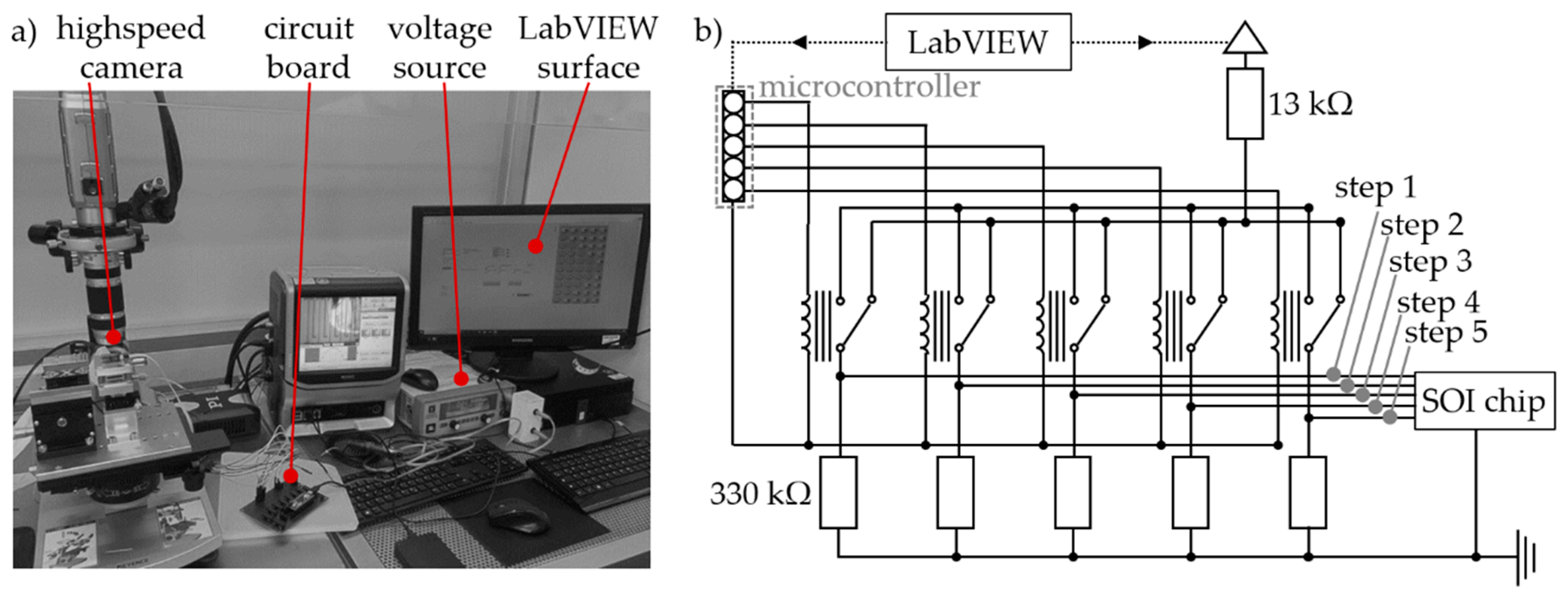
4.1. Experiment and Characterization Setup

The system performance is evaluated using a highspeed camera system (Keyence VW−600C), the actuators are driven by a voltage source (EA—Electro-Automatic PS-3200-02 C), as presented in Figure 8a. A DC voltage is used for the actuation of the bending plate actuators. The actual system displacement is analyzed with the software Tracker. Due to the very high aspect ratio of length vs. displacement and due to the symmetric setup of the system, the videos either investigate the middle, the left or the right side of the system. Experiments are repeated three times under same conditions and averaged.
For the collective actuation, the voltage source is driven by a LabVIEW program increasing the voltage as a function of time. A 13 kΩ resistor limits the current flow in case of a potential breakthrough of the SiN isolation layer at the electrodes.
The printed circuit board (PCB) used for the step-by-step actuation is presented in Figure 8b. A LabVIEW program drives the voltage source as well as a microcontroller (Arduino) that activates a set of double pole relays connected to the electrostatic actuators. The combination of double pole relays with the 330 kΩ resistors allows a quick discharge and therefore a quick release of the electrode beams when deactivating the relays. Based on this setup, sticking problems did not appear during the step-by-step actuation. The LabVIEW program allows an activation of all relays as an arbitrary function of time.

4.2. System Characterization Results

4.2.1. Overview of Results

Table 2 provides an overview of the experimental qualitative and quantitative system characterization results that will be explained and discussed in the following chapters.

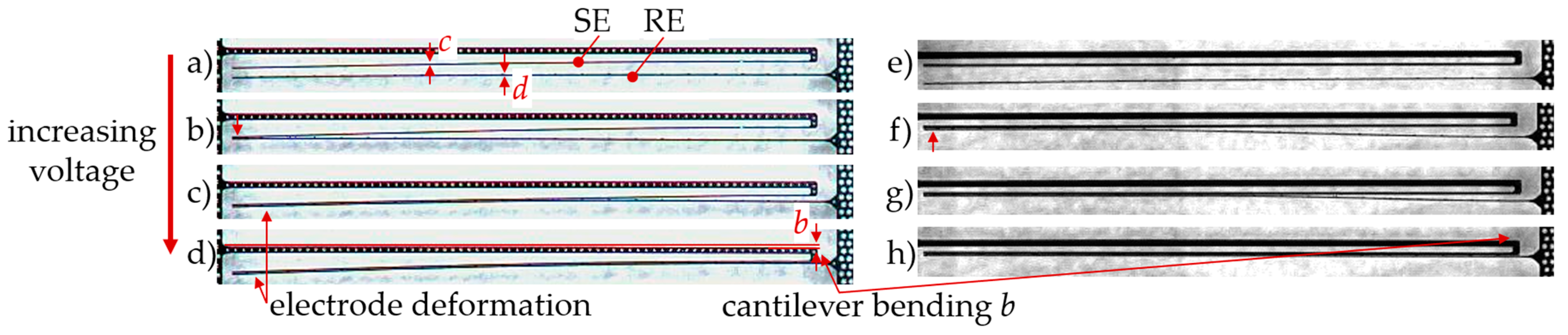
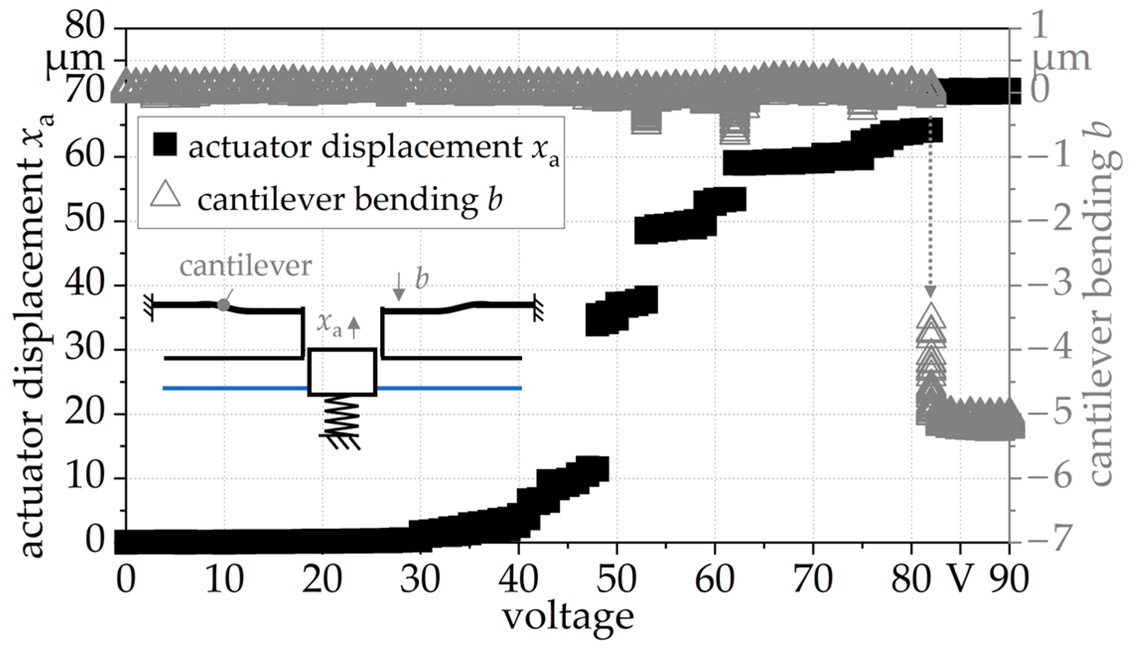
4.2.2. Design-Based Electrostatic Bending Plate Actuator Behavior

Figure 9 shows the influence of the electrode design on the actuator behavior during activation. In Figure 9a, the electrodes feature the same thickness c = d = 5 µm. With increasing voltage, the tips of the electrodes approach due to a bending of the stator electrode. Therefore, the tip of the stator electrode (SE) moves towards the tip of the rotor electrode (RE) (Figure 9b). Then, the electrodes continue their pull-in and start to deform (Figure 9c). The deformation increases with increasing voltage (Figure 9d).
The actuator in Figure 9e features a stator electrode with the thickness c = 10 µm and a rotor electrode with the thickness d = 5 µm. In this case, with increasing voltage, the rotor electrode bends towards the stator electrode due to its lower stiffness (Figure 9f). Thereby, an electrode deformation is not observed. The higher thickness increases the stiffness of the stator electrode, which seems to prevent the undesired electrode deformation observed with the design of Figure 9a. Due to the electrode deformation, the electrodes could get in contact with other system components placed nearby the actuator, which can have a negative influence on the system function. Therefore, the electrostatic actuators of the stepwise systems are designed as presented in Figure 9e.
Figure 10 shows the voltage-dependent experimental displacement of a bending plate actuator and its corresponding cantilever. The voltage is increased in increments of 1 V. Below 30 V, no displacement is observed. At this voltage, the actuator starts displacing, but the cantilever still remains in its position. At 82 V, the cantilever starts to bend down and the pull-in is completed, which can also be seen in Figure 9h. If the cantilever stiffness was higher, the cantilever would not bend and a higher voltage would be required to realize a complete pull-in. During experimental system characterization, the cantilever bending is always the last step leading to a complete pull-in of the bending plate actuators.

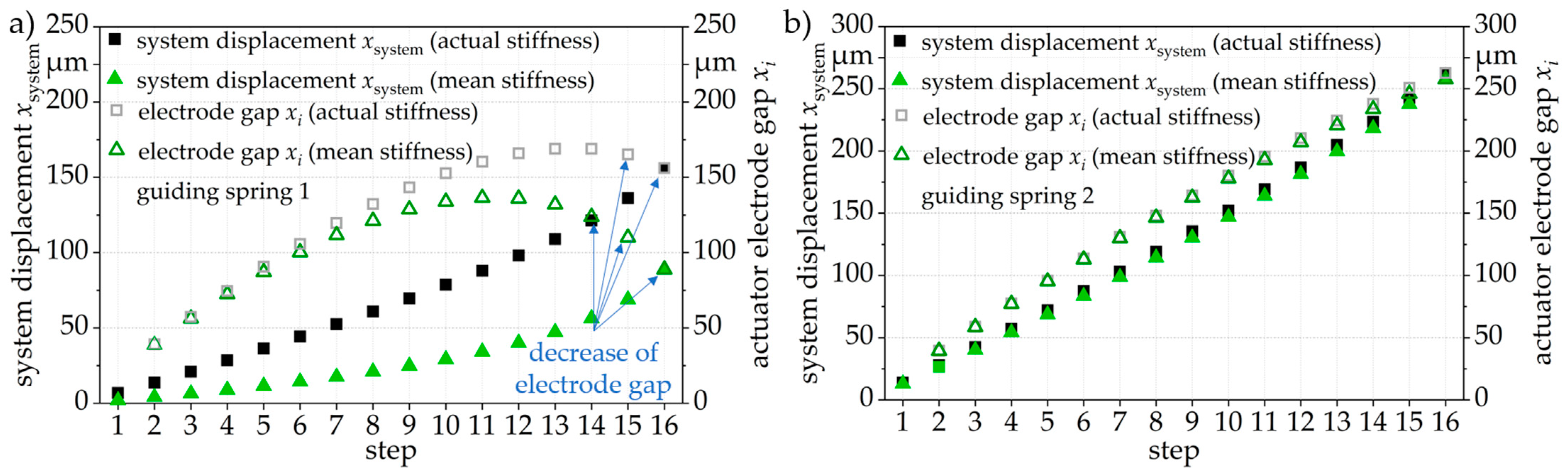
4.2.3. Step-by-Step Actuation of the 5-Step Systems

The step-by-step actuation of system 2 is presented in Figure 11. First, the voltage is increased to 97 V, but all relays on the circuit board remain opened. In Figure 11a, the relays of step 1 are closed which results in a pull-in of step 1. In Figure 11b, the relays of steps 1 to 3 are closed so that the actuators of these steps pull-in. Due to the pull-in of steps 2 and 3, the electrode gaps of steps 4 and 5 decrease. To realize the pull-in of steps 4 and 5, the relays of the corresponding actuators are closed on the PCB (Figure 8b). For the release of the actuators, the relays on the PCB are opened by order again. Thereby, a sticking is prevented due to the double pole relays that are connected to the 330 kΩ resistors, enabling a quick discharge of the electrodes.
The quantitative evaluation of the stepwise system displacement is shown in Figure 11c presenting the total system displacement xsystem,5, depending on the activated steps. The system shows an approximately linear displacement. A comparison with the calculated displacement shows that the analytical model and the experimental results fit very well. The experimentally derived cantilever bending b differs from step to step. For step 1 it amounts to 11.5 µm, for steps 2 to 5 the cantilever bending amounts to 10.1 µm, 10.1 µm, 15.8 µm and 11.0 µm.
To examine the minimum switching speed of the actuators, the LabView program was used to control the time in which the relays on the PCB (Figure 8b) were opened and closed. Thereby, the actuators were successfully deactivated and activated within 1 ms and videos with 1000 fps were taken. Thereby, no sticking of the electrodes was observed which is attributed to the double pole relays combined to the 330 kΩ resistors placed on the PCB (Figure 8b).
Thus, an oscillation of the systems is observed taking about 0.1 s until the oscillation calms down again. To further examine this oscillation, the stepwise activation presented in Figure 11c was repeated, but this time the displacement of each single step was recorded with 500 fps enabling the tracking of the oscillation. Again, the setup with the PCB was used to open and close the double pole relays, and therefore to charge and discharge the actuators. The double pole relays are connected to the single actuators and controlled by a LabView program enabling a time-dependent control of the relays. The single steps are switched every 0.1 s which corresponds to a frequency of 10 Hz. The time-dependent system displacement is shown in Figure 12. When steps 1 and 2 are pulled in, the oscillation of the system decreases, which is attributed to the stiffness of the system which increases with each pulled-in actuator. Comparing Figure 12a,b, System 1 shows a lower oscillation amplitude, which is ascribed to the higher stiffness of its guiding spring.

4.2.4. Comparison of Step-by-Step and Collective Actuation

During collective actuation, the system displacement depends on the applied voltage. The pull-in for actuators with smaller initial electrode gaps is achieved first (Figure 13a), and the actuators with larger electrode gaps follow (Figure 13b). The voltage-dependent displacement of the single steps of the 5-step system during collective actuation is shown in Figure 13c. Thereby, all steps start to displace at the same voltage and every step displaces until its pull-in is completed.
Comparing the step-by-step and the collective actuation, the total system displacement is independent from the mode of activation, contrary to the control voltage. During collective actuation, the electrode tips of the actuators with larger initial electrode gaps already start a movement to each other at low voltage, and therefore reduce the electrode gap of these steps. Consequently, the displacement of the steps with larger initial electrode gaps supports the displacement of steps with smaller initial electrode gaps, resulting in a lower control voltage (Table 2).

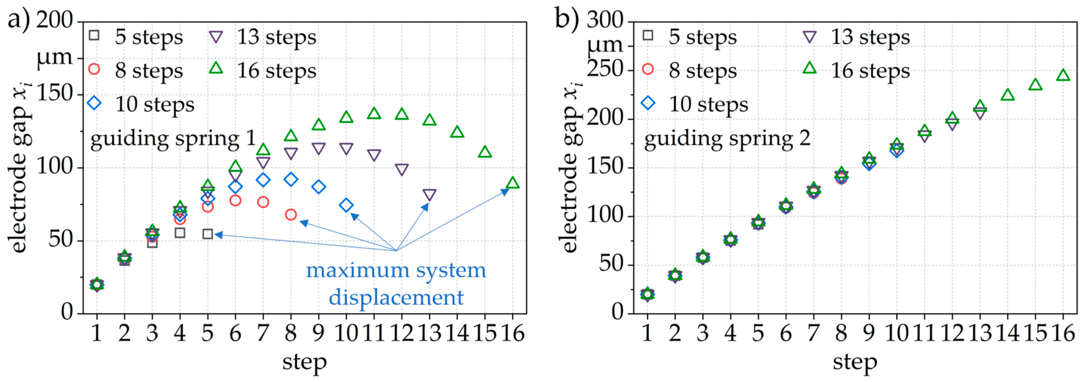
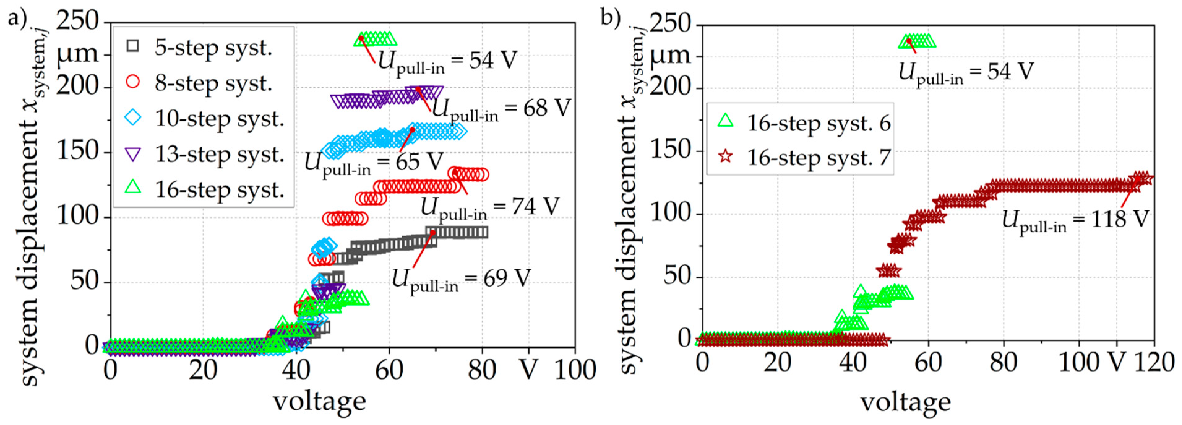
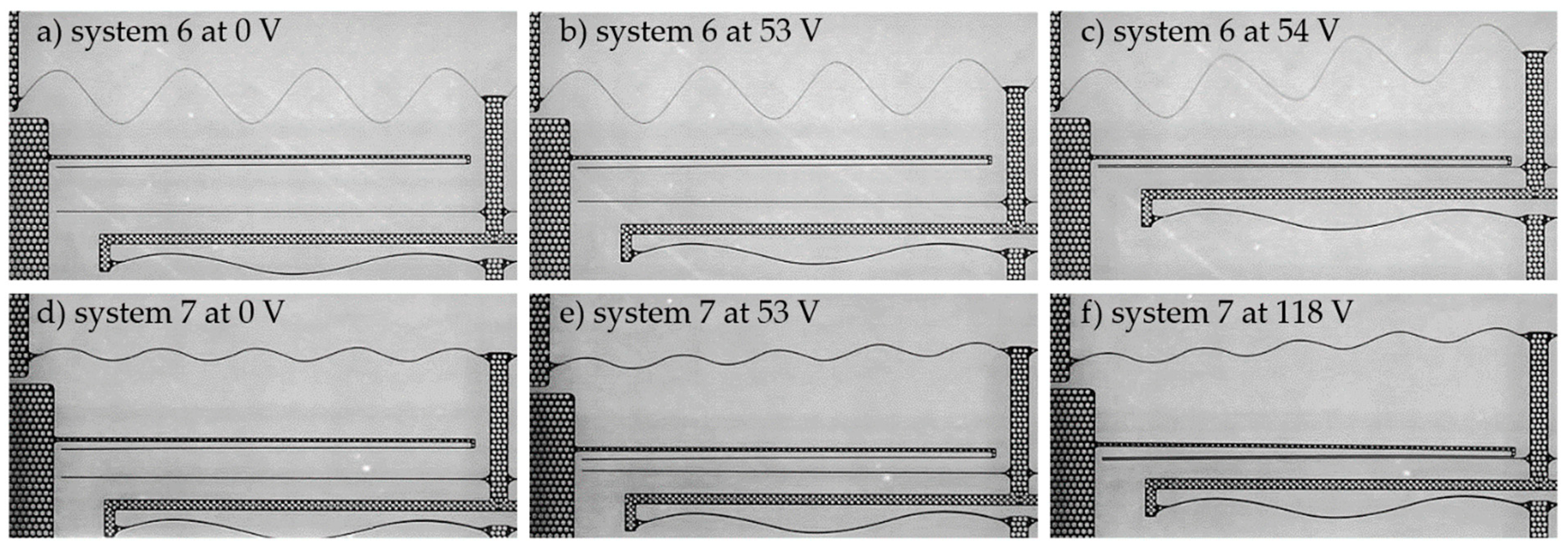
4.2.5. Characterization of Microsystems with 5 to 16 Steps

The systems 2 to 6 only differ in the number of steps and their displacement behavior can easily be compared. Figure 14a shows the voltage-dependent displacement during collective actuation. The systems with more steps achieve a higher displacement. Generally, the pull-in voltage is in the same range and varies between 54 V for the 16-step system and 74 V for the 8-step system.
Table 2 and Figure 14b and Figure 15 show the influence of the guiding spring on the total system displacement. The 16-step systems 6 and 7 differ only in the guiding spring. Nonetheless, the system displacement behavior differs considerably: For system 6 (Figure 15a), the steps 1 to 4 are pulled-in at 53 V (Figure 15b) and at 54 V the pull-in of all steps is completed (Figure 15c). For system 7 (Figure 15d), steps 1 to 12 are pulled in at 53 V (Figure 15e), but for the pull-in of all steps a voltage of 118 V is required (Figure 15f).
The pull-in of the multi-step systems is further analyzed using video analysis. With increasing voltage, the actuators of the 5-step system pull-in one after each other. For the 8-, 10-, and 13-step systems, the actuators partly pull-in at the same voltage which is presented in Table 2. For system 6, the actuators a1 to a4 pull-in in turn with increasing voltage. However, the actuators a5 to a16 pull-in at the same voltage (Figure 14b and Figure 15c). This is attributed to the low stiffness of the guiding spring supporting to conduct an impulse of movement to the following actuators and resulting in a collective pull-in. Furthermore, the high number of interacting electrostatic actuators increases the electrostatic force in the system which is highly facilitating a pull-in.

5. Conclusions

We present the design, fabrication, and experimental characterization of multi-step systems consisting of cooperative electrostatic bending plate actuators and achieving large and stepwise discrete displacements. The systems are modeled based on a derived transfer function with focus on the influence of the guiding spring stiffness on the system function. During experimental characterization, we show the influence of the electrostatic actuator design on the pull-in behavior. By performing step-by-step actuations, we show the fit of our analytic model with the experimental results and we discuss the influence of the guiding spring stiffness on the oscillation of the system. When activating and deactivating the actuators step-by-step, we achieve a minimum switching time of 1 ms. During collective actuation of all electrostatic actuators, the pull-in voltage decreases due to the higher electrostatic force in the microsystem. The 16-step system with low guiding spring stiffness reaches a maximum displacement of 230.7 ± 0.9 µm at 54 V.

Author Contributions

Conceptualization, L.S. and M.H.; methodology, L.S.; software, L.S..; validation, L.S.; formal analysis, L.S.; investigation, L.S.; resources, L.S. and M.H.; data curation, L.S.; writing—original draft preparation, L.S.; writing—review and editing, M.H.; visualization, L.S.; supervision, M.H.; project administration, M.H. and funding acquisition, M.H. All authors have read and agreed to the published version of the manuscript.

Funding

This study was funded by the Deutsche Forschungsgemeinschaft (DFG, German Research Foundation)–Project-ID 287022738–TRR 196, Project C12.

Institutional Review Board Statement

Not applicable.

Informed Consent Statement

Not applicable.

Data Availability Statement

The data can be provided by the author L.S. upon reasonable request.

Acknowledgments

Some segments of the fabrication process were performed at the Center for Interface-Dominated High Performance Materials (ZGH), Ruhr University Bochum.

Conflicts of Interest

The authors declare no conflict of interest. The funders had no role in the design of the study; in the collection, analyses or interpretation of the data; in the writing of the manuscript or in the decision to publish the results.

References

  1. Fu, X.; Yang, F.; Liu, C.; Wu, X.; Cui, T.J. Terahertz Beam Steering Technologies: From Phased Arrays to Field-Programmable Metasurfaces. Adv. Opt. Mater. 2020, 8, 1900628. [Google Scholar] [CrossRef]
  2. Grade, J.D.; Jerman, H.; Kenny, T.W. Design of large deflection electrostatic actuators. J. Micromech. Syst. 2003, 12, 335–343. [Google Scholar] [CrossRef]
  3. Preetham, B.S.; Lake, M.A.; Hoelzle, D.J. A curved electrode electrostatic actuator designed for large displacement and force in an underwater environment. J. Micromech. Microeng. 2017, 27, 095009. [Google Scholar] [CrossRef]
  4. Burugupally, S.P.; Perera, W.R. Dynamics of a parallel-plate electrostatic actuator in viscous dielectric media. In Sensors and Actuators A: Physical; Elsevier: Amsterdam, The Netherlands, 2019; Volume 295, pp. 366–373. [Google Scholar]
  5. Liu, X.; Samfaß, L.; Kolpatzeck, K.; Häring, L.; Balzer, J.C.; Hoffmann, M.; Czylwik, A. Terahertz Beam Steering Concept Based on a MEMS-Reconfigurable Reflection Grating. Sensors 2020, 20, 2874. [Google Scholar] [CrossRef] [PubMed]
  6. Hoffmann, M.; Nüsse, D.; Voges, E. Electrostatic parallel-plate actuators with large deflections for use in optical moving-fibre switches. J. Micromech. Microeng. 2001, 11, 323. [Google Scholar] [CrossRef]
  7. Bakri-Kassem, M.; Mansour, R.R. High tuning range parallel plate MEMS variable capacitors with arrays of supporting beams. In Proceedings of the 19th IEEE International Conference on Micro Electro Mechanical Systems, Istanbul, Turkey, 22–26 January 2006; pp. 666–669. [Google Scholar]
  8. Zhang, J.; Zhang, Z.; Lee, Y.C.; Bright, V.M.; Neff, J. Design and invention of multi-level digitally positioned micromirror for open-loop controlled applications. In Sensors and Actuators A: Physical; Elsevier: Amsterdam, The Netherlands, 2003; Volume 103, pp. 271–283. [Google Scholar]
  9. Velosa-Moncada, L.A.; Aguilera-Cortés, L.A.; González-Palacios, M.A.; Raskin, J.P.; Herrera-May, A.L. Design of a novel MEMS microgripper with rotatory electrostatic comb-drive actuators for biomedical applications. Sensors 2018, 18, 1664. [Google Scholar] [CrossRef] [PubMed] [Green Version]
  10. Leroy, E.; Hinchet, R.; Shea, H. Multimode hydraulically amplified electrostatic actuators for wearable haptics. Adv. Mater. 2020, 32, 2002564. [Google Scholar] [CrossRef] [PubMed]
  11. Legtenberg, R.; Groeneveld, A.W.; Elwenspoek, M. Comb-drive actuators for large displacements. J. Micromech. Microeng. 1996, 6, 320. [Google Scholar] [CrossRef] [Green Version]
  12. Korvink, J.; Oliver, P. MEMS: A Practical Guide of Design, Analysis, and Applications; Springer Science & Business Media: New York, NY, USA, 2010. [Google Scholar]
  13. Dean, R.N.; Wilson, C.; Brunsch, J.P.; Hung, J.Y. A synthetic voltage division controller to extend the stable operating range of parallel plate actuators. In Proceedings of the 2011 IEEE International Conference on Control Applications (CCA), Denver, CO, USA, 28–30 September 2011; pp. 1068–1074. [Google Scholar] [CrossRef]
  14. Chiou, J.C.; Lin, Y.C. A novel capacitance control design of tunable capacitor using multiple electrostatic driving electrodes. In Proceedings of the IEEE-NANO 2001, M3.1 Nanoelectronics and Giga-Scale Systems, Maui, HI, USA, 28–30 October 2001; pp. 319–324. [Google Scholar]
  15. Seeger, J.I.; Boser, B.E. Charge control of parallel-plate, electrostatic actuators and tip-in instability. J. Micromech. Syst. 2003, 12, 656–671. [Google Scholar] [CrossRef] [Green Version]
  16. Lu, M.C.; Fedder, G.K. Position control of parallel-plate microactuators for probe based data storage. J. Micromech. Syst. 2004, 13, 759–769. [Google Scholar] [CrossRef]
  17. Maithripala, D.H.S.; Berg, J.M.; Dayawansa, W.P. Nonlinear dynamic output feedback stabilization of electrostatically actuated MEMS. In Proceedings of the IEEE Conference on Decision and Control, Maui, HI, USA, 9–12 December 2003; Volume 1, pp. 61–66. [Google Scholar]
  18. Schmitt, L.; Schmitt, P.; Hoffmann, M. 3-Bit Digital-to-Analog Converter with Mechanical Amplifier for Binary Encoded Large Displacements. Actuators 2021, 10, 182. [Google Scholar] [CrossRef]
  19. Schmitt, L.; Schmitt, P.; Barowski, J.; Hoffmann, M. Stepwise Electrostatic Actuator System for THz Reflect Arrays. In Proceedings of the International Conference and Exhibition on New Actuator Systems and Applications, Online, 17–19 February 2021; 2021. [Google Scholar]
  20. Schmitt, P.; Schmitt, L.; Tsivin, N.; Hoffmann, M. Highly Selective Guiding Springs for Large Displacements in Surface MEMS. J. Micromech. Syst. 2021. [Google Scholar] [CrossRef]
  21. Overstolz, T.; Clerc, P.A.; Noell, W.; Zickar, M.; de Rooij, N.F. A clean wafer-scale chip-release process without dicing based on vapor phase etching. In Proceedings of the 17th IEEE International Conference on Micro Electro Mechanical Systems. Maastricht MEMS 2004 Technical Digest, Maastricht, The Netherlands, 25–29 January 2004. [Google Scholar]
  22. Sari, I.; Zeimpekis, I.; Kraft, M. A dicing free SOI process for MEMS devices. Microelectron. Eng. 2012, 95, 121–129. [Google Scholar] [CrossRef] [Green Version]
  23. Schmitt, L.; Schmitt, P.; Liu, X.; Czylwik, A.; Hoffmann, M. Micromechanical Reflect-Array for THz Radar Beam Steering based on a Mechanical D/A Converter and a Mechanical Amplifier. In Proceedings of the 2020 Third International Workshop on Mobile Terahertz Systems (IWMTS), Essen, Germany, 1–2 July 2020. [Google Scholar]
Figure 1. (a) Setup of the bending plate actuator, (b) completely pulled-in bending plate actuator, (drawings not to scale).
Actuators 10 00272 g001
Figure 2. (a) Setup of the system, (b) analogous electrical network model, (drawings not to scale).
Actuators 10 00272 g002
Figure 3. (a) 5-step system (system 2) for step-by-step and collective actuation, (b) 16-step system (system 6) for collective actuation, (stacked device photos).
Actuators 10 00272 g003
Figure 4. (a) Geometry of the guiding springs 1 and 2; (b) stiffness of guiding springs 1 and 2 based on solid state COMSOL Multiphysics simulation.
Actuators 10 00272 g004
Figure 5. System displacement and electrode gap distance of 16-step systems depending on mean and actual stiffness value design guided by (a) guiding spring 1 (actual stiffness value: system 7 presented in Table 1), (b) guiding spring 2 (mean stiffness value: system 6 presented in Table 1). The values are obtained analytically (Equations (2) and (3)) by calculating with the spring stiffness values that are obtained by COMSOL simulation. The electrode gap amounts to 20 µm for each actuator.
Actuators 10 00272 g005
Figure 6. Analytically derived electrode gaps for systems with a mean stiffness value design featuring (a) guiding spring 1, (b) guiding spring 2.
Actuators 10 00272 g006
Figure 7. Fabrication process (a) etching of bond pads, (b) deep-etching of handle layer, (c) PECVD of 400 nm SiO2, (d) deep-etching of device layer, (e) HF-vapor etching, (f) deposition of 400 nm SiN, (drawings not to scale).
Actuators 10 00272 g007
Figure 8. (a) Characterization setup in the cleanroom, (b) setup of the printed circuit board.
Actuators 10 00272 g008
Figure 9. Pull-in depending on electrode thickness, (ad) c = d = 5 µm, (eh) c = 10 µm, d = 5 µm, detailed description in the continuous text.
Actuators 10 00272 g009
Figure 10. Displacement of the bending plate actuator and bending of the cantilever depending on the applied voltage, for the actuator of step 5 of system 1.
Actuators 10 00272 g010
Figure 11. Step-by-step actuation of system 2 (left hand side) at 97 V, relays closed at (a) step 1, (b) steps 1 to 3, (c) experimental and analytical displacement of system 2 at 97 V control voltage, Table 2 presents the exact measured results.
Actuators 10 00272 g011
Figure 12. Time-dependent displacement of the single steps at step-by-step activation of (a) system 1, (b) system 2.
Actuators 10 00272 g012
Figure 13. Collective actuation of system 2 at (a) 44 V, (b) 50 V, (c) experimental displacement of the single steps of system 2, the voltage is increased in 1 V-steps every 2 s.
Actuators 10 00272 g013
Figure 14. System displacement depending on applied voltage of the 5-, 8-, 10-, 13- and 16-step systems during collective activation, comparison of (a) systems 2 to 6, (b) system 6 and system 7, the voltage is increased in 1 V-steps every 2 s.
Actuators 10 00272 g014
Figure 15. Voltage-dependent total displacement of the 16-step system 6, at (a) 0 V, (b) 53 V, and (c) 54 V and of the 16-step system 7 at (d) 0 V, (e) 53 V and (f) 118 V.
Actuators 10 00272 g015
Table 1. Modeled systems, the simulated mean stiffness of guiding spring 1 is kg = 2.9 N/m and the simulated stiffness of the the connecting springs is ki = 4.9 N/m.
SystemNumber
of Steps
ActivationDesign/
Stiffness Value
Guiding SpringMax. Calculated
Displacement
Chip Size
[µm × µm]
Presented in Figure
15step-by-step
and collective
mean180 µm6945 × 10,2536a
2 5step-by-step
and collective
actual294 µm6945 × 10,2533a
38collectivemean2143 µm8865 × 91576b
410collectivemean2171 µm10,255 × 91576b
513collectivemean2212 µm12,392 × 91576b
616collectivemean2242 µm14,407 × 91573b, 5b, 6b
716collectiveactual1156 µm14,407 × 91575a
Table 2. Overview of the experimental results that will be discussed in the following chapters.
SystemMax. Experimental
Displacement
Voltage for
Max. Displacement
System Properties
1xsystem,5 = 71.9 ± 0.5 µm82 V (step-by-step)
71 V (collective)
xsystem,1 = 5.9 µm, xsystem,2 = 22.0 µm,
xsystem,3 = 38.5 µm, xsystem,4 = 55.4 µm,
oscillation during step-by-step actuation
2 xsystem,5 = 89.4 ± 0.8 µm97 V (step-by-step)
69 V (collective)
xsystem,1 = 10.6 µm, xsystem,2 = 27.9 µm,
xsystem,3 = 47.3 µm, xsystem,4 = 61.4 µm,
oscillation during step-by-step actuation
3xsystem,8 = 138.4 ± 2.3 µm74 Vpull-in order: a1 + a2, a3 + a4, a5, a6, a7, a8
4xsystem,10 = 168.3 ± 3.1 µm65 Vpull-in order: a1, a2–a7, a8, a9, a10
5xsystem,13 = 202.7 ± 3.6 µm68 Vpull-in order: a1, a2–a4, a5–a8, a9, a10–a12, a13
6xsystem,16 = 230.7 ± 0.9 µm54 Vpull-in order: a1, a2, a3, a4, a5–a16
7xsystem,16 = 138.9 ± 1.7 µm118 Vpull-in order: a1, a2 + a3, a4–a6, a7, a8, a9–a12, a13, a14, a15, a16
Publisher’s Note: MDPI stays neutral with regard to jurisdictional claims in published maps and institutional affiliations.

