Practical Submodule Capacitor Sizing for Modular Multilevel Converter Considering Grid Faults


1
Department of Energy Technology, Aalborg University, 9220 Aalborg, Denmark
2
Nanyang Technological University, Singapore 639798, Singapore
*
Author to whom correspondence should be addressed.
Appl. Sci. 2020, 10(10), 3550; https://doi.org/10.3390/app10103550
Submission received: 5 April 2020
/
Revised: 14 May 2020
/
Accepted: 19 May 2020
/
Published: 20 May 2020
(This article belongs to the Special Issue Advancing Grid-Connected Renewable Generation Systems 2019)
Abstract
:Submodule (SM) capacitors are key elements in the modular multilevel converter (MMC), the design of which influences the entire system performance. In practical cases, SM capacitor sizing must consider the abnormal system operation (e.g., grid faults). In order to find a clear design boundary for SM capacitors, a practical capacitor sizing method is presented for the first time in this paper, considering the grid-fault-ride-through operation of the MMC, impact of MMC control system, and aging mechanism of capacitors. The SM capacitor rated voltage, capacitance, ESR, thermal resistance, and lifetime can be decided to ensure reliable operations of the MMC during grid faults. The effectiveness of the proposed method has been verified through experimental tests on a down-scale MMC system.
1. Introduction
Several commercial modular multilevel converter (MMC) projects have been deployed in the past few decades [1,2,3]. Compared with the traditional line-commutated converter (LCC), the MMC has many competitive advantages, e.g., low switching frequency, high conversion efficiency, strong scalability and reduced harmonic distortion [4,5,6,7,8,9]. As a key part in the MMC, the SM capacitors must achieve high reliability in industrial projects, due to their high-voltage and high-power operating environment. Moreover, according to the national grid code shown in [10], the ability of grid-fault-ride-through is required for grid-tied MMCs. Especially in countries such as Germany and Canada, the converters must stay connected to the grid when a 100% voltage dip [11,12] appears. These unexpected grid fault operation will bring extra voltage stress on SM devices (IGBTs and capacitors), which is one of the critical reasons leading to system-level failure [13,14,15,16]. To avoid this problem, the SM capacitor is normally over-designed in practical cases, causing the rise of size and cost of the overall system. Thus, an optimized SM capacitor sizing method considering grid fault conditions is necessary for the practical MMC design.
Some efforts have been devoted to the SM capacitor sizing to ensure the steady-state operation of MMCs [17,18,19,20]. For instance, an SM capacitor sizing method is given in [17], based on the energy storage requirement of each SM. Dimensioning of SM capacitors considering energy fluctuation, ripple voltage is given in [18]. The minimum size for the SM capacitors to keep their voltage fluctuation is given in [19]. A computational design procedure in the aspects of maximum SM voltage, SM ripple voltage, and current stress is given in [20], considering the impact of the modulation index and the instantaneous power output. However, these methods assume that the system operates in steady-state with normal grid conditions, which cannot be used to predict the SM voltage during grid faults. To solve this problem, the control method of the MMC under unbalanced grid conditions is discussed in [21] and the literature [22] gives the mathematical model of the SM voltage, considering the positive- and negative-sequence of grid voltages and the MMC arm currents.
The above solutions can be used for SM capacitor sizing when the system operates in steady-state. However, the SM voltage is also affected by other factors, such as control strategies, modulation methods, circuit configurations, etc. For instance, the impact of the circulating current suppresion control (CCSC) on SM capacitor voltage ripples under different unbalanced AC grid conditions is discussed in [23]. With a second-order circulating current control [24], the SM voltage ripple can be reduced, i.e., a lower SM capacitance is required. An improved DC-loop regulator is proposed in [25] to suppress the capacitor voltage fluctuations. Considering unbalanced grid conditions, the DC-link voltage ripple is regulated through an arm voltage feed-forward control [26]. The interaction between the MMC modulation methods and the SM voltage stress is discussed in [27]. By applying a power decoupling circuit to each SM, the voltage ripple can be suppressed [28]. Hence, the sizing of SM capacitor should take the system control schemes into consideration.
In addition, the SM capacitor sizing should also consider the transient state of the MMC during grid faults, which may induce catastrophic damage to the SM. To study the transient behavior of MMC system, a few literature works have been conducted [16,29,30]. A time-domain transient SM voltage analysis is shown in [16]. By taking the grid current control into account, the transient SM voltage response during grid faults is discussed in [29]. In Ref. [30], the transient response of CCSC and its impact on SM voltage are analyzed.
Considering the impact factors above, the aim of this paper is ensure the reliability of SM capacitors when the system operates both in normal and grid fault states. Thus, a practical SM capacitor sizing method is proposed in this paper. Accordingly, the SM capacitor rated voltage and capacitance are chosen based on the grid fault operation principle of the MMC, including the transient voltage stress on SM. Moreover, the ESR, thermal resistance, and rated lifetime of the SM capacitor is chosen considering the aspect of reliability requirement. The rest of this paper is structured as follows: Section 2 discusses the operation principles and control schemes of the MMC system. The transient state SM voltage is analyzed in Section 3, where an analytical model is proposed. Design considerations of the MMC system are provided in Section 4, while the SM capacitor selection procedure is given in Section 5. A detailed design example of a down-scale MMC system is given in Section 6, where experimental tests are performed to validate the proposed method. Finally, concluding remarks are presented.
2. Steady-State Analysis of SM Capacitor Voltage
A three-phase MMC topology is shown in Figure 1. Each arm of the MMC contains N identical half-bridge SMs and one series-connected arm inductor La. The SM is formed by two IGBTs and a parallel SM capacitor Csm. The SM voltage vsm is defined as the voltage across each SM capacitor, while the DC-bus voltage is considered as a constant denoted by Vdc.The AC output of the MMC is connected to the grid through a three-phase /Y transformer. Thus, there will not be any zero-sequence currents on the converter side during grid fault conditions.
To simplify the analysis, it is assumed that the voltage across each SM is well-balanced. Thus, an equivalent circuit can be derived for each phase-leg of the MMC, as shown in Figure 2. All the SMs in each arm are combined into a single equivalent capacitor being . The equivalent capacitors hold the total voltage stress of the upper arm vuj and lower arm vlj, where j indicates the phase (j = a, b, c). The switching devices of each SM are replaced by a pair of equivalent controlled-sources. The grid phase voltage and output current of each phase are represented by vj and ij. The circulating current is denoted as icj. The insertion index of the upper and lower arms is represented by nuj and nlj, while the arm current is defined as iuj and ilj. Due to the symmetrical characteristic of the MMC system, only the expression of upper arm is given.
In steady-state, the grid voltage and current of each phase can be expressed as
where is the fundamental line frequency, is the power factor angle, and and are the peak value of grid voltage and current.
The total energy variation of the upper arm is analyzed in [17] with
where m is the modulation index, given by .
Meanwhile, the energy storage in the upper arm can be represented as
Combining Equations (3) and (4), the voltage stress of an SM capacitor in the upper arm can be given as
where
To study the steady-state SM voltage ripple, the waveform of F function under different operating point is shown in Figure 3. Hence, the operating voltage boundary of SM capacitors in steady-state can be obtained as
where Fmax and Fmin are the maximum and minimum value of the F function.
3. Transient SM Capacitor Voltage during Grid Faults
3.1. System Dynamics and Control Schemes
Based on Figure 2, the dynamics of an MMC can be described as
where vcj is the voltage driving the circulating current through each phase-leg, and vsj is the differential voltage controlling the current injected into the grid. Accordingly, vcj and vsj are given as
By applying the Park transformation on Formula (10), the output current dynamic can be described in the dq-frame as
where , , , and are the positive- and negative-sequence components of in the dq-frame.
According to Equations (15) and (16), a typical output control loop can be constructed for the MMC as shown in Figure 4. A positive-sequence control and a negative-sequence control using PI regulators are adopted, where Kop and Ki are the gains. The positive- and negative-sequence components of the grid voltage can be extracted with methods in [31] and used as the input of a grid current reference generator, which is applied to provide the active and reactive current references (, , , ) for the controller.
According to Equation (14), a circulating current suppression control (CCSC) of the MMC can be designed as shown in Figure 5 [14]. A PR controller is applied to eliminate the dominant double-line frequency ripple in the circulating current, where Kcp and Kr represent its gains. The DC reference of the circulating current control will be given by a circulating current reference generator.
3.2. Grid Fault SM Voltage Estimation
Based on the dynamics of the SM voltage shown in Equation (11), the SM voltage stress of each phase-leg is governed by the arm currents (iuj and ilj) and its insertion indexes (nuj and nlj). According to Equation (12), the arm currents are composed of the circulating current and phase output current.
As shown in Figure 4, the state functions of the positive current sequence can be represented as
where
in which and .
According to Formula (17), the transfer functions of the positive-sequence current can be written as with matrix . Based on this method, the transfer functions of output current control can be represented as
in which , , , are given in Formula (19), respectively:
To describe the system dynamics during grid faults, Table 1 indicates the operation point of the MMC system during normal state and grid fault conditions. By applying the reverse Laplace transformation on Equation (18), the time-domain transient response of the system in the dq-frame can be obtained as
where the input of the system can be regarded as a series of step signals in the s-domain
According to [32], the dynamics of the output current can be calculated as
By applying the direct modulation [33], the insertion indexes of the upper and lower arms can be calculated as
According to Equation (11), the dynamic response of the total SM voltage can be obtained as
where is the initial time of the grid fault. As the voltage across each SM in the same arm is assumed to be balanced, the voltage stress on each SM can be given as
Thus, the maximum SM voltage stresses during the grid fault transient can be predicted as
4. Design Consideration of SM Capacitors
4.1. Energy Storage Requirement
According to [17], the energy stored in each arm of the MMC must be larger than the required energy by the grid. In steady-state, the required inserted voltage for the upper arm can be expressed as
By substituting Equation (31) into (5), the energy requirement of SM capacitor can be given as
By taking Equation (3) into (32), the required SM capacitance for each phase-leg can be obtained as
4.2. SM Ripple Voltage Requirement
To ensure the stability and efficiency of the MMC, the SM voltage ripple must be kept in a safe range during steady-state operation. Defining the allowable peak-to-peak voltage ripple as , the following condition should be satisfied:
Solving Equation (34) yields the minimum capacitance requirement as
4.3. Transient SM Voltage Constraint
For industrial MMC projects, a series of protection strategies are embedded in the control system to avoid switching devices (e.g., IGBTs) getting over-stressed. Once the operating SM voltage reaches a preset threshold , the SM will be bypassed by the control blocks [34]. If a large amount of SMs get over-charged at the same time, a system-level shutdown may be triggered. Thus, the transient SM voltage must be constrained under the threshold , which can be written as .
By substituting Equations (27) and (28) into the equation, it can be obtained as
It should be noted that the maximum transient SM voltage for upper and lower arms can be different during grid faults. The selected SM capacitance should fulfill the Equations (49) and (50) in the meantime.
4.4. ESR, Thermal Resistance, and Lifetime Assessment
To ensure a long-term reliable operations of the MMC, the thermal stresses of SM capacitors must be evaluated. According to [35], a simple lifetime model of SM capacitors can be given as
where is the lifetime of the capacitor under rated voltage and testing temperature ; the exponent is normally selected from 7 to 9.4 for metallized polypropylene film (MPPF) capacitor; is the operating hot-spot temperature of the capacitors.
In order to study the thermal behavior of the SM capacitors, a lumped thermal model of film capacitors are given in Figure 6 [36], where the steady-state hot-spot temperature of capacitors can be expressed as
The thermal resistance of the capacitor Rth relates to the material of the capacitor. Ta is the ambient temperature, Ploss is the power losses of the SM capacitor.
By neglecting the harmonics on the circulating current, the SM capacitor charging current can be decomposed by a fundamental line frequency component and a double-line frequency component, which can be expressed as [37]
With different modulation index and phase angle, the RMS value of is shown in Figure 7, while the RMS value of equals . Thus, the power losses for SM capacitors can be calculated as
where is the equivalent-series-resistance (ESR) of the SM capacitor under fundamental line frequency, is the ESR under double line frequency.
5. SM Capacitor Selection
5.1. SM Capacitance Selection
According to Equations (33), and (35)–(37), the design boundary of the SM capacitance can be obtained. Considering the capacitance losses caused by aging of capacitors [38], an extra design margin must be guaranteed. Thus, the SM capacitance can be chosen as
where is the redundancy factor of SM capacitance selection. Normally, is chosen from 1.2 to 2.
5.2. Rated Voltage Selection
According to characteristics of film capacitors [39], the peak value of the operating voltage must not exceed their rated DC voltage. Thus, the rated voltage of the SM capacitor can be chosen as
where the maximum voltage stress on SM capacitors can be calculated according to Equations (10) and (38)–(42).
5.3. Design Flowchart
Based on the analysis above, a design procedure flowchart is shown in Figure 8. First, some basic parameters are required, which includes the DC-link voltage (), number of SMs in each arm (N), arm inductance (), AC-side fundamental angular frequency (), gain of the MMC control loops (, and ) allowable peak-to-peak SM voltage ripple (), maximum SM voltage threshold (), expected SM capacitor lifetime (), and system operating points in normal and grid fault conditions. Then, the minimum SM capacitance that satisfies the energy storage, voltage ripple, and transient SM voltage requirements can be calculated using the Equations (33) and (35)–(37). After that, the SM capacitance can be decided by adding a proper redundancy to the highest value among , , . Based on the selected capacitance, the rated voltage of SM capacitor can be obtained using Formula (45). Since the capacitance and rated voltage have been decided, a certain type of capacitor product can be selected in the market. In the end, the lifetime of the selected capacitor product needs to be checked using Equations (38) and (43). It should be noted that the MMC system may encounter different fault conditions. Thus, this design process may be conducted multiple times based on different grid fault operating points. Through comparison, the maximum calculation value of and can be chosen as the final result.
6. Case Study
6.1. Design Example
To verify the correctness of the proposed method, a down-scale three-phase MMC design case is given. Key system parameters and design requirement were as shown in Table 2. The maximum SM voltage ripple should be limited within 10% of the SM DC-bias, while the allowable SM voltage is selected 25% higher than the SM DC-bias. Two common grid fault conditions are selected for SM capacitor sizing: single-line-to-ground fault and three-phase short-circuit fault. Both positive- and negative-sequence currents will be injected into the grid when the grid fault is detected. The reactive current injection strategy follows the German grid code, as shown in [40]. Thus, the MMC operating points during the normal state and grid fault conditions are shown in Table 3.
By putting the design parameters above into Formulas (33) and (35), the SM capacitance demand for energy storage requirement and ripple voltage requirement can be calculated as: F, F. According to Equations (38)–(39), the relationship between SM capacitance and the maximum transient SM voltage stress can be calculated and shown in Figure 9. To keep the SM voltage in a safety range during both grid fault conditions, is selected as 1.14 mF. With a 20% extra design margin (), the final SM capacitor is chosen as 1.36 mF, formed by two 680 F capacitors connecting in parallel. By setting the rated voltage of the SM capacitor at 100 V, the information of the selected product is given in Table 4. By taking the ESR value into Formula (43), the power losses of the SM capacitor is around 0.1 W, which is relatively small. Thus, the hot-spot temperature of the SM capacitor is considered as equal to the ambient temperature in this case study. Assuming the operating ambient temperature is 60 C, the SM capacitor lifetime can be estimated using Equation (51) as h.
6.2. Experimental Verification
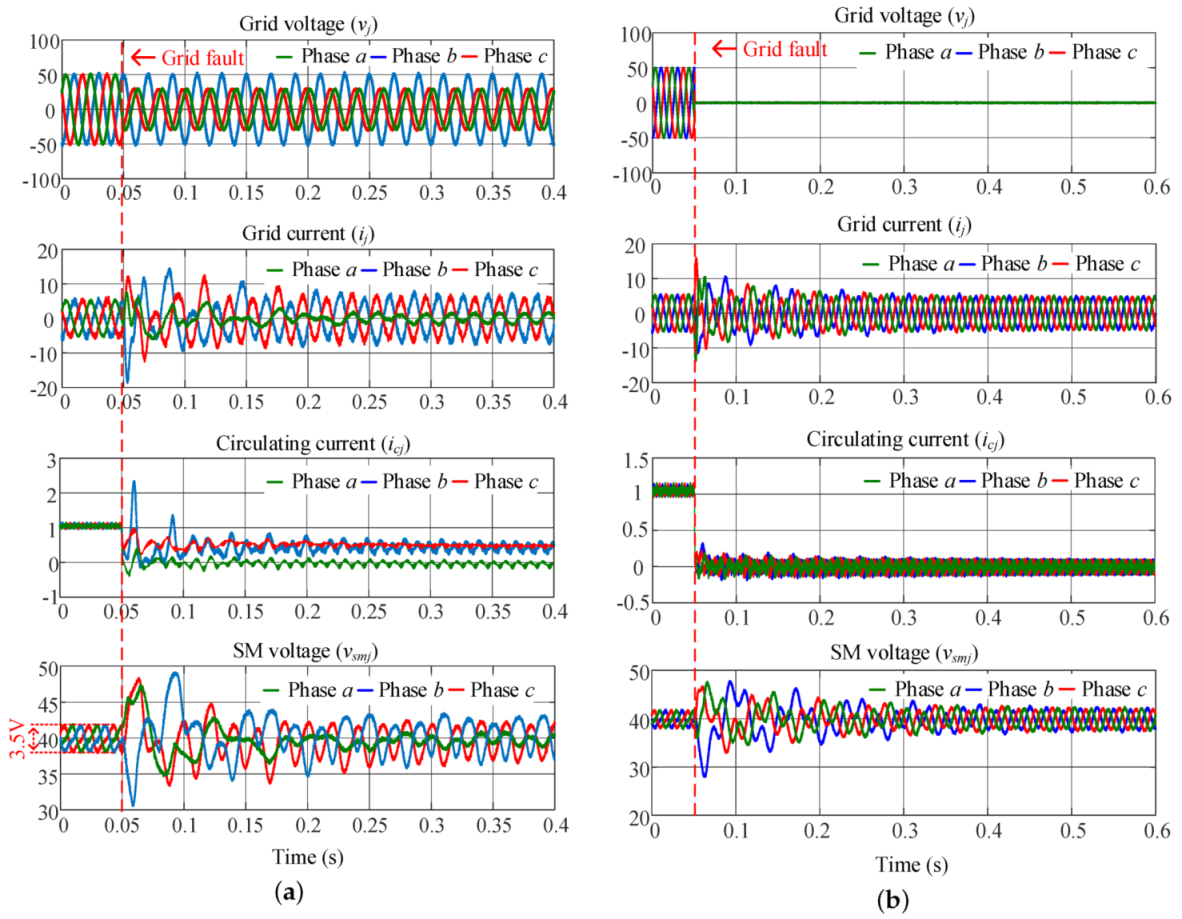
By using the selected components given in Table 4, an experiment platform has been assembled, the structure of which is shown in Figure 10. The platform is formed with three phase-legs. The DC-side voltage of the MMC is provided by a constant DC source. A dSPACE system is used as the controller of the MMC, while an auxiliary DC supply is used to provide power for the sensors and gate drivers in the system. The AC side of the platform is connected to a grid simulator, which is used to generate the grid fault signal. The system operation waveforms during grid fault conditions are shown in Figure 11, where the system state during single-line-to-ground condition and three-phase short-circuit condition is shown in Figure 11a,b, respectively. Due to the symmetrical characteristic, only the SM voltage of upper arm is given.
It can be seen that the circulating current through each phase-leg is well-suppressed when the system operates in steady-state. During normal operation, the peak-to-peak SM voltage ripple is 3.5 V, which is well constrained within the design limit. During the transient state of both grid fault conditions, an obvious voltage over-shoot appears on each SM capacitor, which is caused by the dynamic response of the control system [30]. In Figure 11a, the maximum SM voltage in three phase-legs is 48.8 V, which is 1.5 V higher than the model-estimated value shown in Figure 9a. For three-phase short circuit condition, the maximum SM voltage is close to the expectation, with only a 1 V difference. These estimation errors are caused by the signal coupling within the MMC control system. However, all SM voltage is limited under 40 V, which proves the effectiveness of the proposed SM capacitor selection method.
7. Conclusions
A straightforward practical SM capacitor sizing method is proposed in this paper for MMC systems. Compared with the existing solutions, the proposed method is more applicable for a grid-connected MMC project, especially for cases requiring grid-fault-ride-through ability, such as static synchronous compensator (STATCOM) and the MMC-based HVDC system. A reliable path is given to select the capacitance, rated voltage, ESR, thermal resistance, and rated lifetime of the SM capacitor, considering the system requirement during normal operation state and grid-fault-ride-through conditions. Through analyzing the control loop, a quantitative estimation method of the maximum voltage stresses was given, which provides an insight into the impact of different control schemes on the SM capacitor design and improves the reliability of the MMC operating under grid fault conditions. A down-scale MMC experimental platform is designed and assembled. By comparing the experiment results with the design requirement, all design parameters are well achieved, which proves the effectiveness of the proposed design method.
Author Contributions
Z.Y. is mainly in charge of the conceptualization, methodology, theoretical modelling, and manuscript preparation. H.Q. is involved in the process of software programming and data acquisition. Y.T., Y.Y., and H.W. contribute to the project administration and supervision. All authors have read and agreed to the published version of the manuscript.
Funding
This research received no external funding.
Conflicts of Interest
The authors declare no conflict of interest.
References
- Pang, H.; Wei, X. Research on Key Technology and Equipment for Zhangbei 500kV DC Grid. In Proceedings of the International Power Electronics Conference (ECCE Asia), Niigata, Japan, 20–24 May 2018; pp. 2343–2351. [Google Scholar]
- Ou, K.; Rao, H.; Cai, Z.; Guo, H.; Lin, X.; Guan, L.; Maguire, T.; Warkentin, B.; Chen, Y. MMC-HVDC Simulation and Testing Based on Real-Time Digital Simulator and Physical Control System. IEEE J. Emerg. Sel. Top. Power Electron. 2014, 2, 1109–1116. [Google Scholar]
- ABB Solusion. Available online: https://new.abb.com/systems/hvdc/hvdc-light (accessed on 20 May 2020).
- Akagi, H. Classification, Terminology, and Application of the Modular Multilevel Cascade Converter (MMCC). IEEE Trans. Power Electron. 2011, 26, 3119–3130. [Google Scholar] [CrossRef]
- Dekka, A.; Wu, B.; Fuentes, R.L.; Perez, M.; Zargari, N.R. Evolution of Topologies, Modeling, Control Schemes, and Applications of Modular Multilevel Converters. IEEE J. Emerg. Sel. Top. Power Electron. 2017, 5, 1631–1656. [Google Scholar] [CrossRef]
- Perez, M.A.; Bernet, S.; Rodriguez, J.; Kouro, S.; Lizana, R. Circuit Topologies, Modeling, Control Schemes, and Applications of Modular Multilevel Converters. IEEE Trans. Power Electron. 2015, 30, 4–17. [Google Scholar] [CrossRef]
- Nami, A.; Liang, J.; Dijkhuizen, F.; Demetriades, G.D. Modular Multilevel Converters for HVDC Applications: Review on Converter Cells and Functionalities. IEEE Trans. Power Electron. 2015, 30, 18–36. [Google Scholar] [CrossRef]
- Debnath, S.; Qin, J.; Bahrani, B.; Saeedifard, M.; Barbosa, P. Operation, Control, and Applications of the Modular Multilevel Converter: A Review. IEEE Trans. Power Electron. 2015, 30, 37–53. [Google Scholar] [CrossRef]
- Ilves, K.; Antonopoulos, A.; Norrga, S.; Nee, H. Steady-State Analysis of Interaction Between Harmonic Components of Arm and Line Quantities of Modular Multilevel Converters. IEEE Trans. Power Electron. 2012, 27, 57–68. [Google Scholar] [CrossRef]
- Iov, F.; Hansen, A.D.; Sorensen, P.; Cutululis, N.A. Mapping of Grid Faults and Grid Codes; Tech. Rep. Riso-R-1617 (EN); Riso National Laboratory, Technical University of Denmark: Roskilde, Denmark, 2007. [Google Scholar]
- VDN—Transmission Code 2003; Network and System Rules of the German Transmission System Operators: Berlin, Germany, 2003.
- Hydro-Quebec Technical Information. Available online: http://www.hydroquebec.com/transenergie/fr/commerce/pdf/exigence_raccordement_fev_09_en.pdf (accessed on 20 May 2020).
- Shi, X.; Wang, Z.; Liu, B.; Liu, Y.; Tolbert, L.M.; Wang, F. Characteristic Investigation and Control of a Modular Multilevel Converter-Based HVDC System Under Single-Line-to-Ground Fault Conditions. IEEE Trans. Power Electron. 2015, 30, 408–421. [Google Scholar] [CrossRef]
- Li, J.; Konstantinou, G.; Wickramasinghe, H.R.; Pou, J. Operation and Control Methods of Modular Multilevel Converters in Unbalanced AC Grids: A Review. IEEE J. Emerg. Sel. Top. Power Electron. 2019, 7, 1258–1271. [Google Scholar] [CrossRef]
- Li, G.; Liang, J.; Ma, F.; Ugalde-Loo, C.E.; Liang, H. Analysis of Single-Phase-to-Ground Faults at the Valve-Side of HB-MMCs in HVDC Systems. IEEE Trans. Ind. Electron. 2019, 66, 2444–2453. [Google Scholar] [CrossRef]
- Nademi, H.; Norum, L. Analytical circuit oriented modelling and performance assessment of modular multilevel converter. IET Power Electron. 2015, 8, 1625–1635. [Google Scholar] [CrossRef]
- Ilves, K.; Norrga, S.; Harnefors, L.; Nee, H. On Energy Storage Requirements in Modular Multilevel Converters. IEEE Trans. Power Electron. 2014, 29, 77–88. [Google Scholar] [CrossRef]
- Bärnklau, H.; Gensior, A.; Bernet, S. Submodule Capacitor Dimensioning for Modular Multilevel Converters. IEEE Trans. Ind. Appl. 2014, 50, 1915–1923. [Google Scholar] [CrossRef]
- Merlin, M.M.C.; Green, T.C. Cell capacitor sizing in multilevel converters: Cases of the modular multilevel converter and alternate arm converter. IET Power Electron. 2015, 8, 350–360. [Google Scholar] [CrossRef]
- Tang, Y.; Ran, L.; Alatise, O.; Mawby, P. Capacitor Selection for Modular Multilevel Converter. IEEE Trans. Ind. Appl. 2016, 52, 3279–3293. [Google Scholar] [CrossRef]
- Guan, M.; Xu, Z. Modeling and Control of a Modular Multilevel Converter-Based HVDC System Under Unbalanced Grid Conditions. IEEE Trans. Power Electron. 2012, 27, 4858–4867. [Google Scholar] [CrossRef]
- Shi, X.; Wang, Z.; Liu, B.; Li, Y.; Tolbert, L.M.; Wang, F. Steady-State Modeling of Modular Multilevel Converter Under Unbalanced Grid Conditions. IEEE Trans. Power Electron. 2017, 32, 7306–7324. [Google Scholar] [CrossRef]
- Li, J.; Konstantinou, G.; Wickramasinghe, H.R.; Pou, J.; Wu, X.; Jin, X. Impact of Circulating Current Control in Capacitor Voltage Ripples of Modular Multilevel Converters Under Grid Imbalances. IEEE Trans. Power Deliv. 2018, 33, 1257–1267. [Google Scholar] [CrossRef]
- Zhao, C.; Lei, M.; Hu, Y.; Li, Z.; Gao, F.; Wang, P.; Li, Y. Energy Storage Requirement Optimization of Hybrid Modular Multilevel Converter With Circulating Current Injection. IEEE Trans. Ind. Electron. 2019, 66, 6637–6648. [Google Scholar] [CrossRef]
- Li, B.; Zhang, Y.; Wang, G.; Sun, W.; Xu, D.; Wang, W. A Modified Modular Multilevel Converter With Reduced Capacitor Voltage Fluctuation. IEEE Trans. Ind. Electron. 2015, 62, 6108–6119. [Google Scholar] [CrossRef]
- Tu, Q.; Xu, Z.; Chang, Y.; Guan, L. Suppressing DC Voltage Ripples of MMC-HVDC Under Unbalanced Grid Conditions. IEEE Trans. Power Deliv. 2012, 27, 1332–1338. [Google Scholar] [CrossRef]
- Picas, R.; Ceballos, S.; Pou, J.; Zaragoza, J.; Konstantinou, G.; Agelidis, V.G. Closed-Loop Discontinuous Modulation Technique for Capacitor Voltage Ripples and Switching Losses Reduction in Modular Multilevel Converters. IEEE Trans. Power Electron. 2015, 30, 4714–4725. [Google Scholar] [CrossRef] [Green Version]
- Kong, Z.; Huang, X.; Wang, Z.; Xiong, J.; Zhang, K. Active Power Decoupling for Submodules of a Modular Multilevel Converter. IEEE Trans. Power Electron. 2018, 33, 125–136. [Google Scholar] [CrossRef]
- Yin, Z.; Yang, Y.; Wang, H. Transient Voltage Stress Modeling for Submodules of Modular Multilevel Converters under Grid Voltage Sags. In Proceedings of the International Power Electronics Conference (ECCE Asia), Niigata, Japan, 20–24 May 2018; pp. 1021–1026. [Google Scholar]
- Yin, Z.; Qiu, H.; Yang, Y.; Tang, Y.; Wang, H. Impact of the Circulating Current Control on Transient Submodule Voltage Stresses for Grid-Tied Modular Multilevel Converters During Grid Faults. In Proceedings of the IEEE Energy Conversion Congress and Exposition (ECCE), Portland, OR, USA, 23–27 September 2018; pp. 1–6. [Google Scholar]
- Guo, X.; Liu, W.; Zhang, X.; Sun, X.; Lu, Z.; Guerrero, J.M. Flexible Control Strategy for Grid-Connected Inverter Under Unbalanced Grid Faults Without PLL. IEEE Trans. Power Electron. 2015, 30, 1773–1778. [Google Scholar] [CrossRef] [Green Version]
- Jamshidifar, A.; Jovcic, D. Small-Signal Dynamic DQ Model of Modular Multilevel Converter for System Studies. IEEE Trans. Power Deliv. 2016, 31, 191–199. [Google Scholar] [CrossRef] [Green Version]
- Siemaszko, D.; Antonopoulos, A.; Ilves, K.; Vasiladiotis, M.; Ängquist, L.; Nee, H. Evaluation of control and modulation methods for modular multilevel converters. In Proceedings of the International Power Electronics Conference (ECCE ASIA), Sapporo, Japan, 21–24 June 2010; pp. 746–753. [Google Scholar]
- Deng, F.; Zhu, R.; Liu, D.; Wang, Y.; Wang, H.; Chen, Z.; Cheng, M. Protection Scheme for Modular Multilevel Converters Under Diode Open-Circuit Faults. IEEE Trans. Power Electron. 2018, 33, 2866–2877. [Google Scholar] [CrossRef] [Green Version]
- Wang, H.; Blaabjerg, F. Reliability of Capacitors for DC-Link Applications in Power Electronic Converters—An Overview. IEEE Trans. Ind. Appl. 2014, 50, 3569–3578. [Google Scholar] [CrossRef] [Green Version]
- AVX Medium Power Film Capacitors datasheet. Available online: http://datasheets.avx.com/ffli.pdf (accessed on 20 May 2020).
- Marzoughi, A.; Burgos, R.; Boroyevich, D.; Xue, Y. Steady-state analysis of voltages and currents in modular multilevel converter based on average model. In Proceedings of the Energy Conversion Congress and Exposition (ECCE), Montreal, QC, Canada, 20–24 September 2015; pp. 3522–3528. [Google Scholar]
- Soliman, H.; Wang, H.; Blaabjerg, F. A Review of the Condition Monitoring of Capacitors in Power Electronic Converters. IEEE Trans. Ind. Appl. 2016, 52, 4976–4989. [Google Scholar] [CrossRef]
- Vishay Technical Information. Available online: https://www.vishay.com/docs/26033/gentechinfofilm.pdf (accessed on 20 May 2020).
- Sharifabadi, K.; Harnefors, L.; Nee, H.P.; Norrga, S.; Teodorescu, R. Design, Control and Application of Modular Multilevel Converters for HVDC Transmission Systems; Wiley-IEEE Press: Piscataway, NJ, USA, 2016. [Google Scholar]
Figure 1.
Schematic of a three-phase modular multilevel converter.

Figure 2.
Equivalent circuit of each phase-leg of the MMC.

Figure 3.
Waveforms of the F function with (a) , m = 0.6, 0.8, 1 and (b) m = 1, .

Figure 4.
Positive- and negative-sequence current control of the MMC.

Figure 5.
The circulating current control of the MMC.

Figure 6.
A lumped thermal model of SM capacitors.

Figure 7.
The RMS value of at different operating points.

Figure 8.
Design flowchart of SM capacitors.
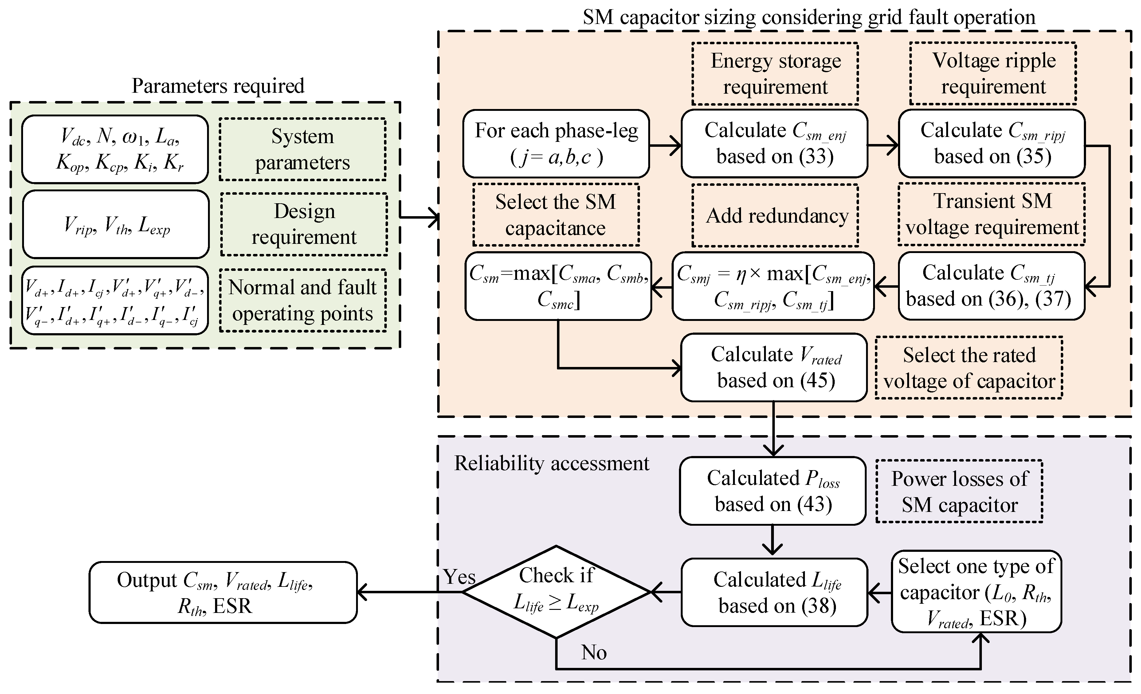
Figure 9.
The maximum SM voltage under different grid faults: (a) single-line-to-ground condition and (b) three-phase short-circuit condition.
Figure 9.
The maximum SM voltage under different grid faults: (a) single-line-to-ground condition and (b) three-phase short-circuit condition.

Figure 10.
A photo of the down-scale MMC experimental platform.

Figure 11.
The experiment waveform of the MMC platform under different grid faults: (a) single-line-to-ground condition and (b) three-phase short-circuit condition.
Figure 11.
The experiment waveform of the MMC platform under different grid faults: (a) single-line-to-ground condition and (b) three-phase short-circuit condition.

Table 1.
Quiescent operation point of the MMC.
| Normal Operation Point | Grid Fault Operation Point |
|---|---|
| = | = |
| = 0 | = |
| = 0 | = |
| = 0 | = |
| = | = |
| = 0 | = |
| = 0 | = |
| = 0 | = |
| = | = |
Table 2.
System parameters and design requirement.
| System Parameters | |
|---|---|
| SM number in each arm (N) | 3 |
| Arm Inductance (La) | 5 mH |
| Grid frequency | 50 Hz |
| Switching frequency | 8 kHz |
| DC-bus voltage | 120 V |
| Kop | 10 |
| Ki | 60 |
| Kcp | 5 |
| Kr | 35 |
| Design Requirement | |
| Peak-to-peak SM voltage ripple (Vrip) | 4 V |
| Maximum SM voltage threshold (Vth) | 50 V |
| Capacitance redundancy factor () | 1.2 |
Table 3.
Possible operation points of the MMC.
| Normal Operation Point | |
|---|---|
| Grid voltage | = 50 V |
| Grid current injection | = 5 A; = 0 |
| Circulating current reference | = 0.417 A |
| Single-Line-to-Ground Condition | |
| Grid voltage | = 33.5 V |
| = 16.5 V | |
| Grid current injection | = 1.67 A |
| = 2.875 A | |
| = 0; = −3.5 A | |
| Three-Phase Short-Circuit Condition | |
| Grid voltage | = 0; = 0 |
| Grid current injection | = 0; = 4.5 A |
| = 0; = 0 | |
Table 4.
Key parameters of the selected capacitor product.
| Part Number | UBY2A681MHL |
|---|---|
| Capacitance | 680 F |
| ESR | 28 m at 50 Hz; 14 m at 100 Hz |
| Thermal resistance | 1.5 C/W |
| Reference lifetime | 3000 h at 125 C, 20–50 V |
© 2020 by the authors. Licensee MDPI, Basel, Switzerland. This article is an open access article distributed under the terms and conditions of the Creative Commons Attribution (CC BY) license (http://creativecommons.org/licenses/by/4.0/).
Share and Cite
MDPI and ACS Style
Yin, Z.; Qiu, H.; Yang, Y.; Tang, Y.; Wang, H. Practical Submodule Capacitor Sizing for Modular Multilevel Converter Considering Grid Faults. Appl. Sci. 2020, 10, 3550. https://doi.org/10.3390/app10103550
AMA Style
Yin Z, Qiu H, Yang Y, Tang Y, Wang H. Practical Submodule Capacitor Sizing for Modular Multilevel Converter Considering Grid Faults. Applied Sciences. 2020; 10(10):3550. https://doi.org/10.3390/app10103550
Chicago/Turabian StyleYin, Zhijian, Huan Qiu, Yongheng Yang, Yi Tang, and Huai Wang. 2020. "Practical Submodule Capacitor Sizing for Modular Multilevel Converter Considering Grid Faults" Applied Sciences 10, no. 10: 3550. https://doi.org/10.3390/app10103550
Note that from the first issue of 2016, this journal uses article numbers instead of page numbers. See further details here.