Article

A Study on the Influence of the Cross-Sectional Shape of the Metal-Inserted Retainer Ring and the Pressure Distribution from the Multi-Zone Carrier Head to Increase the Wafer Yield

1
Department of Mechanical Engineering, Korea Polytechnic University, 237 Sangidaehak-ro, Siheung-Si, Gyeonggi-do 15073, Korea
2
Daegu Research Center for Medical Devices and Rehabilitation, Korea Institute of Machinery and Materials, Daegu 42994, Korea
*
Author to whom correspondence should be addressed.
Co-first author, these authors contributed equally to this work.
Appl. Sci. 2020, 10(23), 8362; https://doi.org/10.3390/app10238362
Submission received: 30 October 2020 / Revised: 21 November 2020 / Accepted: 23 November 2020 / Published: 25 November 2020
(This article belongs to the Section Mechanical Engineering)

Abstract

:
In this paper, for the purpose of increasing the wafer yield by controlling the non-uniformity of the material removal rate during the chemical mechanical polishing process, the influence of the cross-sectional shape of the metal-inserted retainer ring and the pressure distribution on the wafer and the retainer ring generated from the multi-zone carrier head are investigated. First, in order to verify the finite element analysis model, it is correlated using the test data. By using a validated finite element model, simulation studies involving several parameters are performed to reduce the irregularity in the wafer: (1) tapered bottom of the retainer ring, (2) machining round corners at the bottom of the retainer ring, (3) the changes in pressure applied to the wafer, (4) the changes in pressure applied to the retainer ring.

1. Introduction

Chemical mechanical polishing (CMP) is the process of flattening the wafer by lowering the level of the insulating film. In the CMP process, as shown in Figure 1, the polishing process is achieved via the chemical removal reaction due to the chemical composition in the slurry, which is abrasive particles, and the mechanical polishing action between the pad and the wafer by the applied load from the carrier.
It is ideal that the wafer is polished equally at all locations after the CMP process. However, for several reasons, within wafer non-uniformity (WIWNU) occurs and one of the reasons is the rebound phenomenon of the polishing pad [1]. The rebound phenomenon is caused by the release of the pressure applied to the retainer ring, which is a replacement part used for preventing the separation of the wafer during the CMP process, at the edge of the wafer. As a result, the rebound of the pad causes a high contact pressure in the wafer edge area. For this reason, it is impossible to produce semiconductor devices in the edge region, and this edge region of the wafer where the non-uniformity has occurred should be removed. In order to increase the yield of the wafer, it is necessary to predict the material removal rate (MRR) of the wafer and the non-uniformity within the wafer. Several theoretical and empirical studies have been conducted to reduce the wafer non-uniformity and increase the wafer yield [1].
Preston’s equation, expressed as a linear equation of pressure and relative velocity, was presented as a general formula representing the MRR of a wafer in the CMP process [2]. Many studies have been conducted to analyze the MRR based on the Preston equation.
Xu et al. [3] studied the effect of the slurry component on the MRR and WIWNU, and Park et al. [4] conducted a study on the effect of the slurry temperature on the MRR. Bae et al. [5] analyzed the MRR with consideration of the viscoelasticity of the polishing pad made of polyurethane.
Lo et al. [6] applied the finite element method to analyze the ratio of the pressure applied to the wafer and the retainer ring, which can minimize WIWNU, using linear regression equations. Park et al. [7] studied the effect on WIWNU by adjusting the contact angle between the retainer ring and the polishing pad. Park et al. [8] analyzed the effect of platen speed and pressure on the MRR and the wafer surface roughness. Fu et al. [9] pointed out that even if the pressure distribution on the wafer surface was uniformly applied by the carrier, the contact pressure between the wafer and the polishing pad could be non-uniform. Eamkajornsiri et al. [1] investigated the correlation between the curvature of the polishing pad caused by the pressure applied to the wafer and the contact pressure between the wafer and the polishing pad and thus suggested that non-uniformity can be controlled by adjusting the curvature. In order to reduce the non-uniformity of the MRR, a multi-zone carrier head was developed that can transfer various distributed pressure, unlike the conventional head that transfers the uniform pressure on the wafer [10]. Wang et al. [11,12] showed that it is possible to control the non-uniformity of the MRR by making the contact pressure between the wafer and the pad uniform by applying the multi-zone carrier head. In addition, it was found that if the number of the multi-zone by the multi-zone carrier head is increased, non-uniformity can be more effectively controlled.
Recently, various shapes of retainer rings have been proposed to reduce the polishing deviation, and a retainer ring in which metal is inserted has been developed [13]. Based on this, a study on the effect of the material of the retainer ring and the inner ring on the polishing accuracy was recently published [14,15].
In this paper, the effect of the shape changes of the retainer ring with metal inserted and pressure changes via a multi-pressure carrier head were studied. First, in order to verify the finite element model, the existing test data were analyzed and correlated by confirming that the finite element analysis results had the same tendency as the experimental result. Then, for the purpose of increasing the yield of the wafer, it was shown that the non-uniformity can be controlled by adjusting parameters such as the taper angle on the lower part of the retainer ring, the rounded size at the bottom corners of the retainer ring, the pressure applied to the edge area of the wafer, and the changes in pressure applied to the retainer ring. To the best knowledge of the authors, few studies have been conducted on the effects of the cross-sectional shape of the retainer ring inserted with metal and the influence of pressure changes from the multi-zone carrier head.

2. Finite Element Model Verification

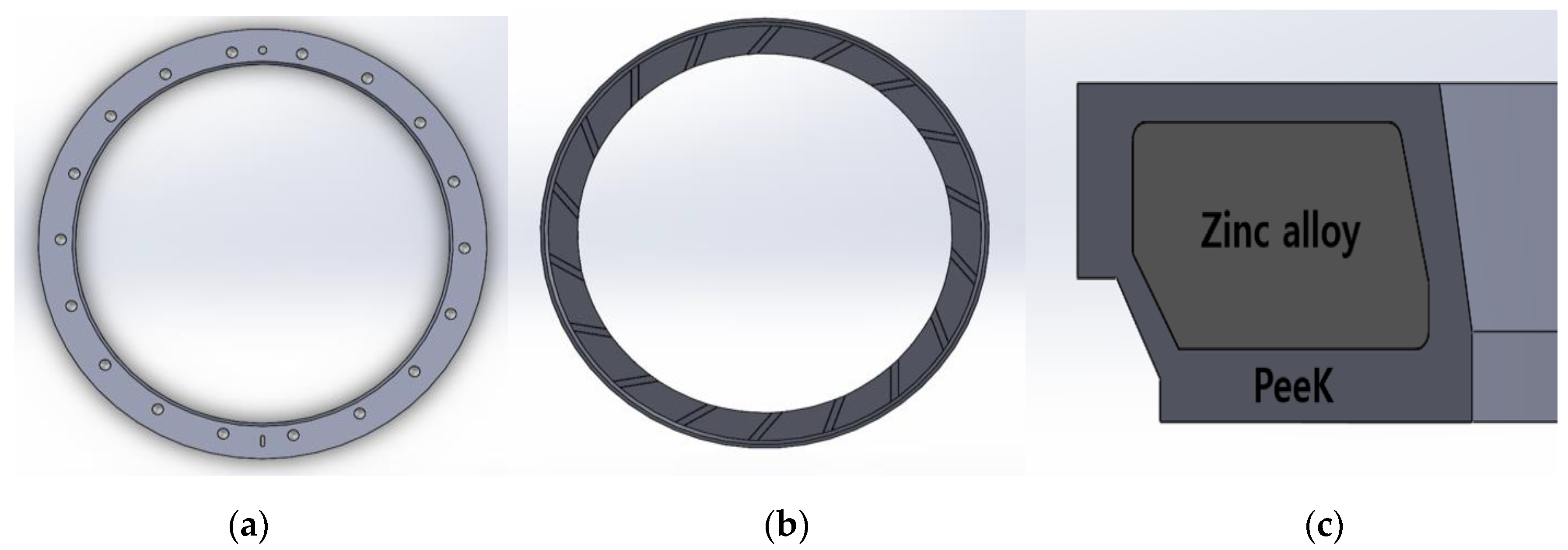
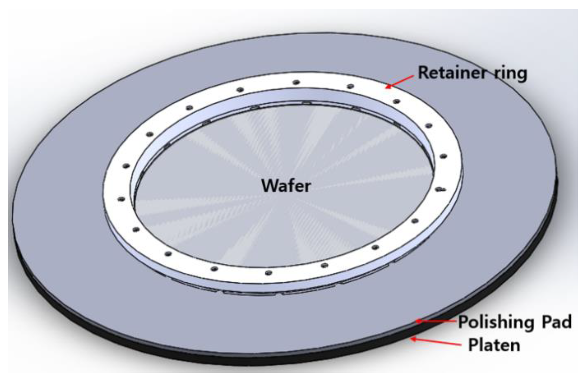
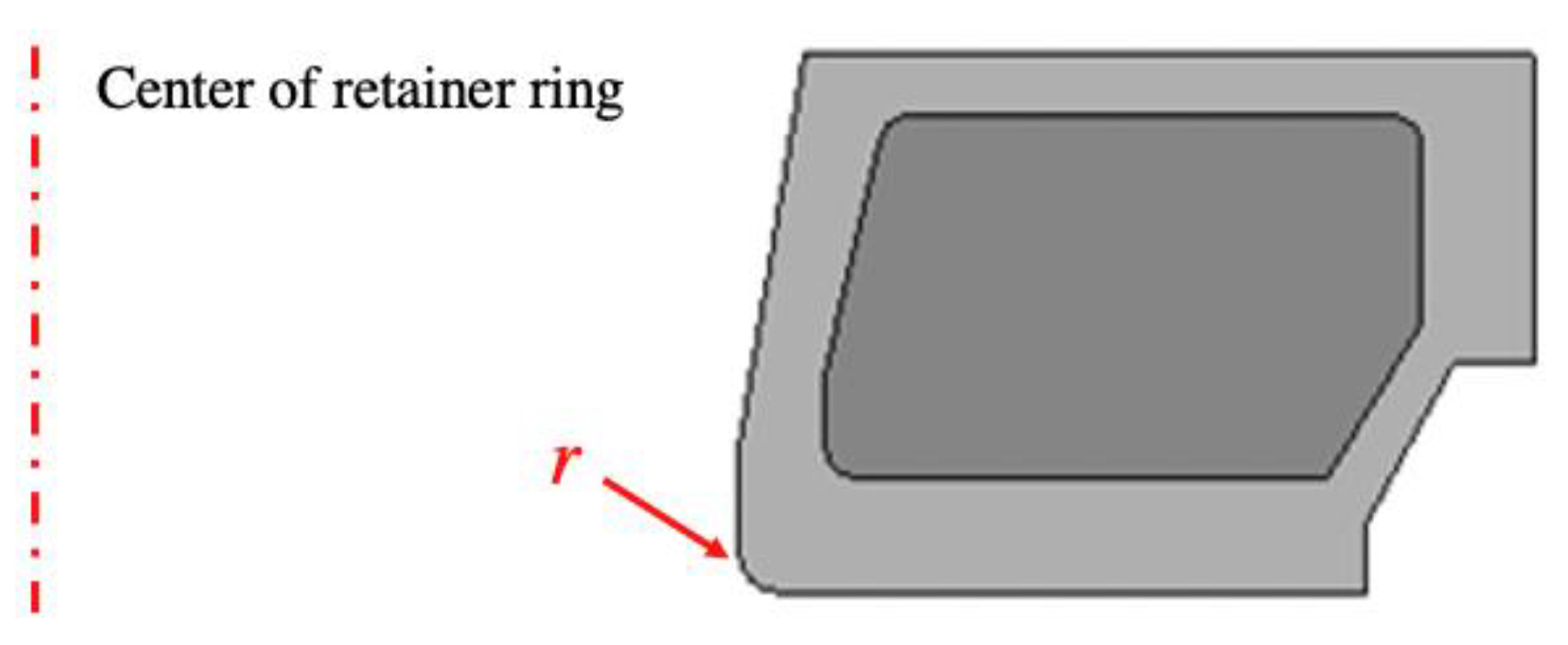
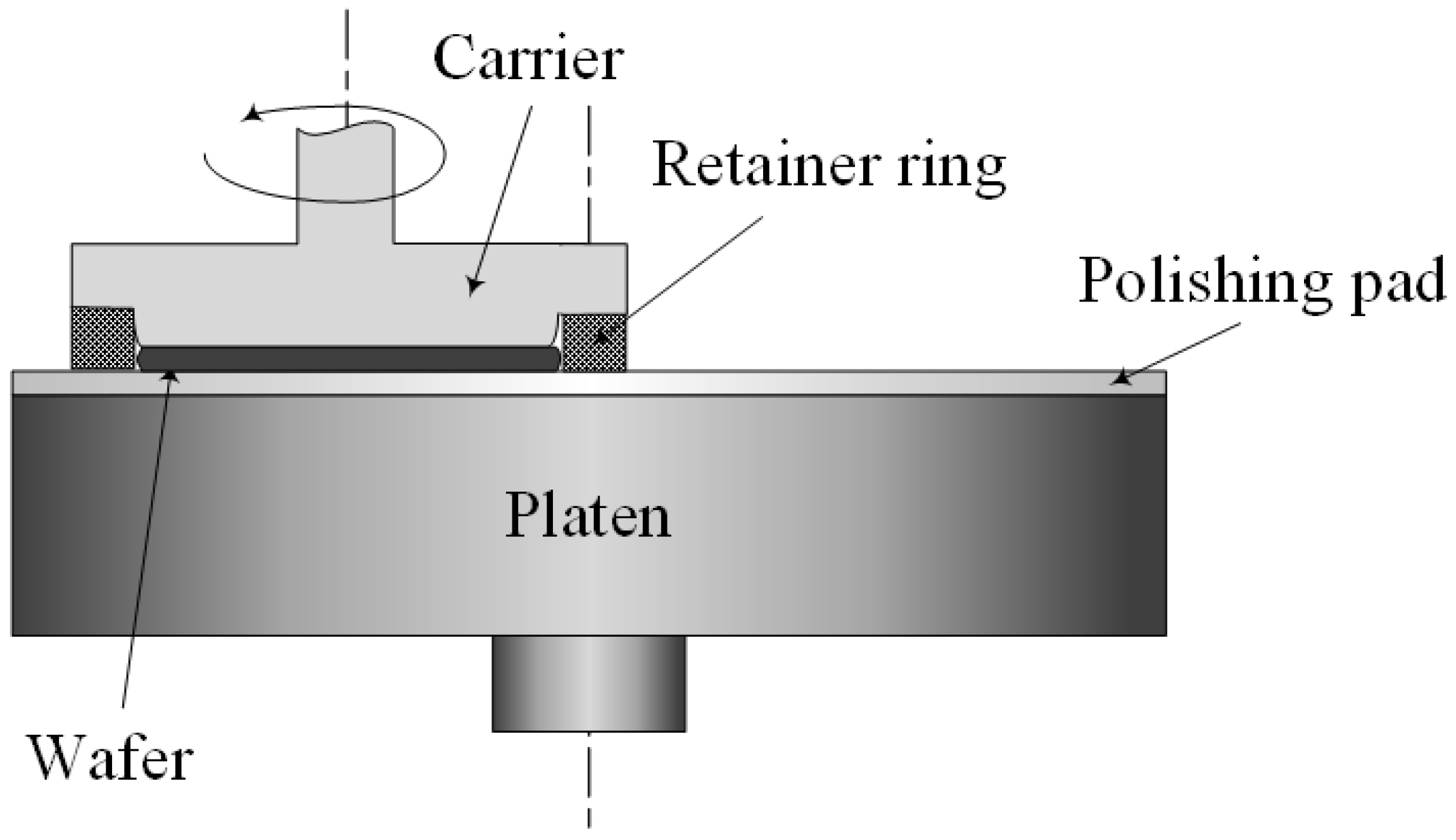
2.1. Structure of Retainer Ring

Figure 2 shows the shape and cross section of the retainer ring, respectively. A retainer ring in which the inner metal is inserted is used, the inner ring is made of zinc alloy, and the material of the outer retainer ring is PEEK (Polyether ether ketone). In the lower part of the retainer ring in contact with the polishing pad, there are grooves that control the inflow and outflow of slurry [14].

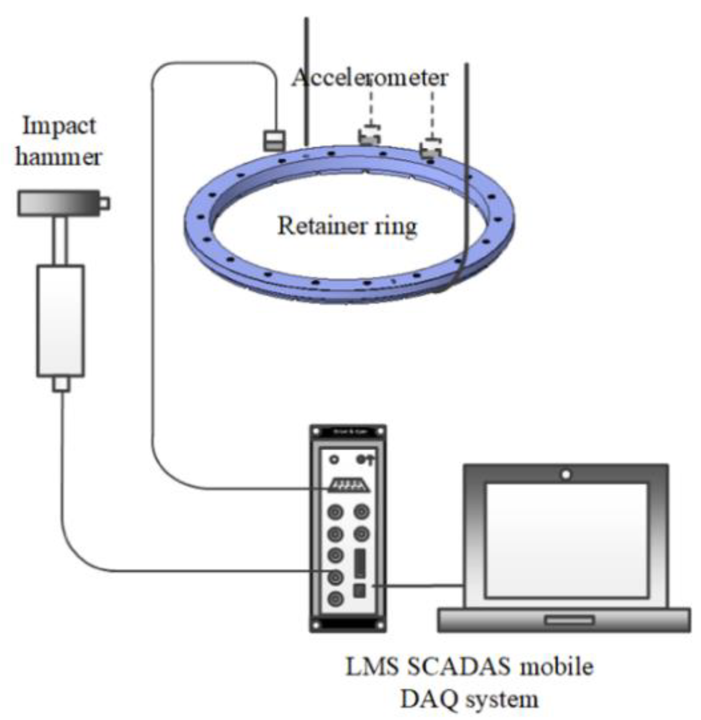
2.2. Analysis of Exsisting Test Data

In order to verify the finite element analysis model, experimental data in the CMP process for several retainer rings were provided courtesy of Will Be S&T Corp. The MRR value of the wafer was obtained after the CMP process using the thin film thickness measurement system (SL-5030 manufactured by K-MAC Ltd., Daejeon, Korea). Since the authors’ laboratories did not have a CMP tester and a thin film thickness measurement system, so a well-organized test for this paper could not be performed. For this reason, this test data was not used for validating the suggested final results of this paper, but for verifying the finite element analysis model.
The cross section information of each retainer ring used in the test is shown in Figure 3. Different pressures were applied for each section from the multi-zone carrier head on the back of the wafer, and detailed information is shown in Table 1. The test was carried out by applying a pressure of 11.9 psi to the retainer ring and 9.3/4.4/4.5/4.5/4.7 psi in Zone 1 to 5, respectively. The test results for the six samples are shown in Figure 4 and Table 2. Using a thin film measurement system, each MRR was measured from the center of the wafer to the left and right. Thus, two results were obtained for one sample. Plus, two samples were produced and tested for the one case. Totally, four results were obtained for one sample. Since the overall MRR values are different for each sample, the average is calculated from the center of the wafer to the 120 mm distance from the center where the MRR values are relatively constant. Then, the relative displacement from the average is calculated and shown in Figure 4 and Table 2. In Table 2, in addition to the maximum relative MRR (MRMRR), the relative MRR at 7 mm distance from the wafer end (RMRR@7mm) was also added since some semiconductor manufacturers empirically remove the edge of the wafer by 7 mm.
By comparing the MRR data of model #1, which is a basic model, and models #2, #3, and #4 with grooves added, the effect of adding a groove can be investigated. As can be seen in Table 2, the grooves generally make the MRR worsen at the wafer edge. By comparing the MRR data of model #2 and model #3, the effect of machining the round shapes can be identified. Since the deviation of the test data is not small, it is even hard to draw a conclusion, but the MRR worsens a little within the error rage. It is estimated that the contact area is reduced by the round shapes. It will be investigated further through a finite element analysis model. In addition, by comparing the MRR data of model #2 with a groove width of 8 mm and model #4 with a groove width of 12 mm, it can be confirmed that the MRR worsens due to the increase in groove size. It is estimated that as the contact area between the retainer ring and the pad decreases, the pressure applied from the retainer ring to the pad increases, resulting in a larger rebound of the pad and non-uniformity. Model #5, in which the inner diameter of the retainer ring was reduced from 301 mm to 300.5 mm, generates the worst result, and it is estimated that the rebound effect is increased as the retainer ring becomes closer to the wafer. As shown in Table 2, by comparing the MRR data of model #2 and model #6 with the same groove width of 8 mm, it can be concluded that the MRR improves as the groove moves away from the wafer center. The reason is estimated to be because the contact pressure on the wafer increases as the location of the groove is closer to the wafer. In addition, it can be seen that cross-sectional change of the retainer ring affects the MRR in the section of about 110–150 mm from the center of the wafer. From the center of the wafer to a distance of about 110 mm, as shown in Figure 4, it can be observed that all models from #1 to #6 show almost the same behavior.
In the case of the upper and lower two-piece type retainer rings, the applied pressure (P1) in zone 1 adjacent to the wafer edge was dominant in the MRR [16]. In order to confirm the influence of the MRR on the pressure change in zone 1, P1 is reduced from 9.3 psi to 6.0 psi based on the #4 model, and the changes in MRR distribution are shown in Figure 5 and Table 3. It can be seen that the non-uniformity of the MRR is improved as P1 is decreased. However, when P1 is too low such as 6.0 psi, non-uniformity is rather deteriorated, and it is estimated that there may be an optimal P1 value.

2.3. Building Up Finite Element Model

Material properties required for finite element analysis were extracted through an experimental method. Density was measured using a digital balance, and Young’s modulus was estimated through the modal test, as shown in Figure 6. The natural frequencies and the corresponding mode shapes were obtained through the modal test. Young’s modulus was corrected so that the modal frequency calculated from the finite element analysis had the same natural frequency obtained by the modal test. Table 4 shows the corrected material properties used in the finite element analysis model. The material properties of wafer, pad, and platen were used by the manufacturer-provided values since no further experiments for material property estimation such as modal tests could be performed.
The finite element analysis was conducted using ABAQUS. The finite element model consists of a pad, retainer ring, wafer, and platen, as shown in Figure 7. Since the rebound phenomenon mainly occurs due to the static interaction between the pad, wafer, and retainer ring, it is attempted to explain this phenomenon only with static analysis. The boundary conditions and load conditions of the analysis model are as follows. A fix boundary condition is applied to the lower part of the platen, and a contact condition is considered between the polishing pad and the wafer and between the polishing pad and the retainer ring with a friction coefficient of 0.1 [17] by referring to the Stribeck Curve. Tie constraint conditions are used between the platen and the polishing pad and between the retainer ring and the inner metal. Each pressure is applied to the wafer through the multi-zone carrier head, and each applied area is shown in Table 1. The load applied from the multi-zone carrier head to the wafer and the retainer ring is considered only for the vertical load.
There are several uncertainties of the finite element model. First, since the real retainer ring rotates in the CMP process, there may be some discrepancy between the actual response and the result from the finite element analysis. In addition, the pressure applied to the wafer in the finite element model may be slightly different from the actual pressure applied to the wafer through the membrane from the multi-zone carrier head. Therefore, through the finite element analysis, it is mainly observed whether the trend of the MRR results is consistent or not.
As shown in Figure 2, the actual model of the retainer ring is not completely an axisymmetric shape because there is a groove. However, when analyzing with a full 3D model, the displacement value of the wafer at the same distance from the center of the wafer is not constant, as shown in Figure 8. Therefore, in order to obtain meaningful data, it is required to extract the data in a circumferential direction, as show in Figure 8, and perform an arithmetic mean. However, this method was too time-consuming because it required a lot of time to analyze the full 3D model and extract the data in the circumferential direction. For the 3D model, after several attempts to obtain a stable value for the mesh size, the mesh size was reduced until the finite element analysis results converged and set, as shown in Table 5. For the element type, the hexahedral mesh was used as much as possible, and the tetrahedral mesh was used in areas where it was impossible to use hexahedral mesh due to its complex geometry shape. Denser meshes were used in the contact area. When considering the analysis time based on a computer (Intel Core-i7, 64GB RAM), enough number of elements could not be used in the case of 3D models, so, in this paper, as shown in Figure 9, a two-dimensional, axisymmetric model was used to reduce the analysis time and use a sufficient number of elements. In Figure 10, the results of analysis with the 2D axisymmetric model and 3D model are compared. For the analysis results of the 3D model, the calculated data obtained through arithmetic averaging after extracting analysis results in the circumferential direction for elements located at the same distance from the wafer center mentioned above is used. In Figure 10, the analysis result of the 2D axisymmetric model has no significant difference from the analysis result of the 3D model, and this paper intends to improve the WIWNU through trend analysis using the finite element analysis results, so the finite element analysis was performed using a 2D axisymmetric model.

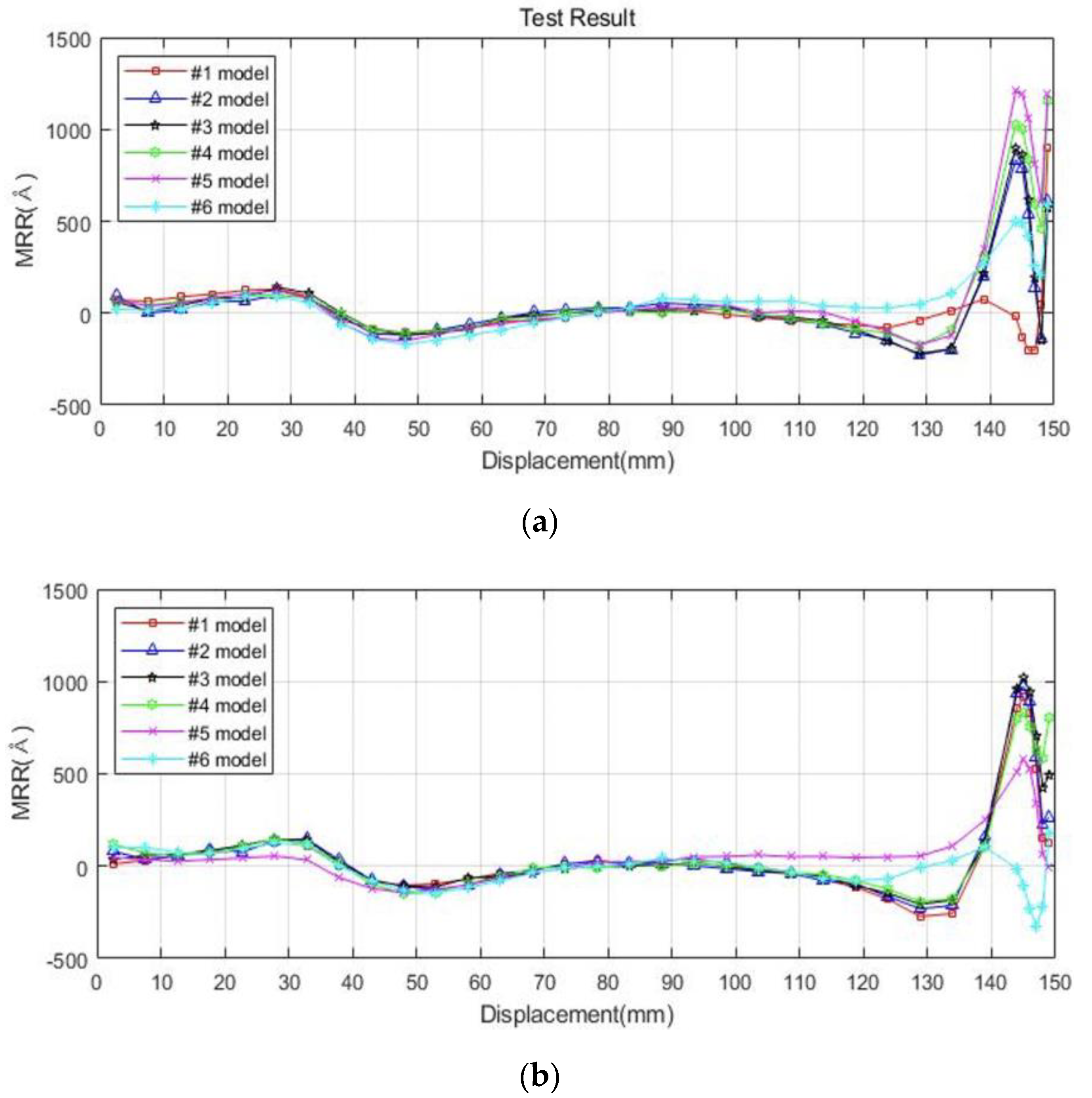
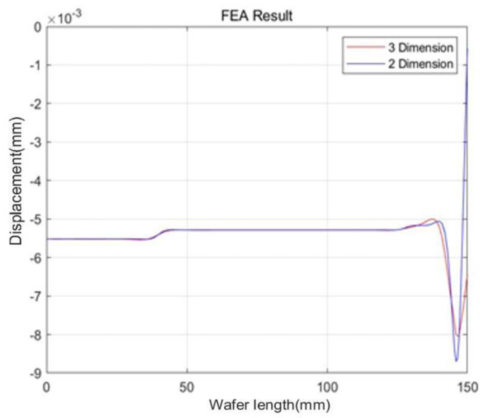
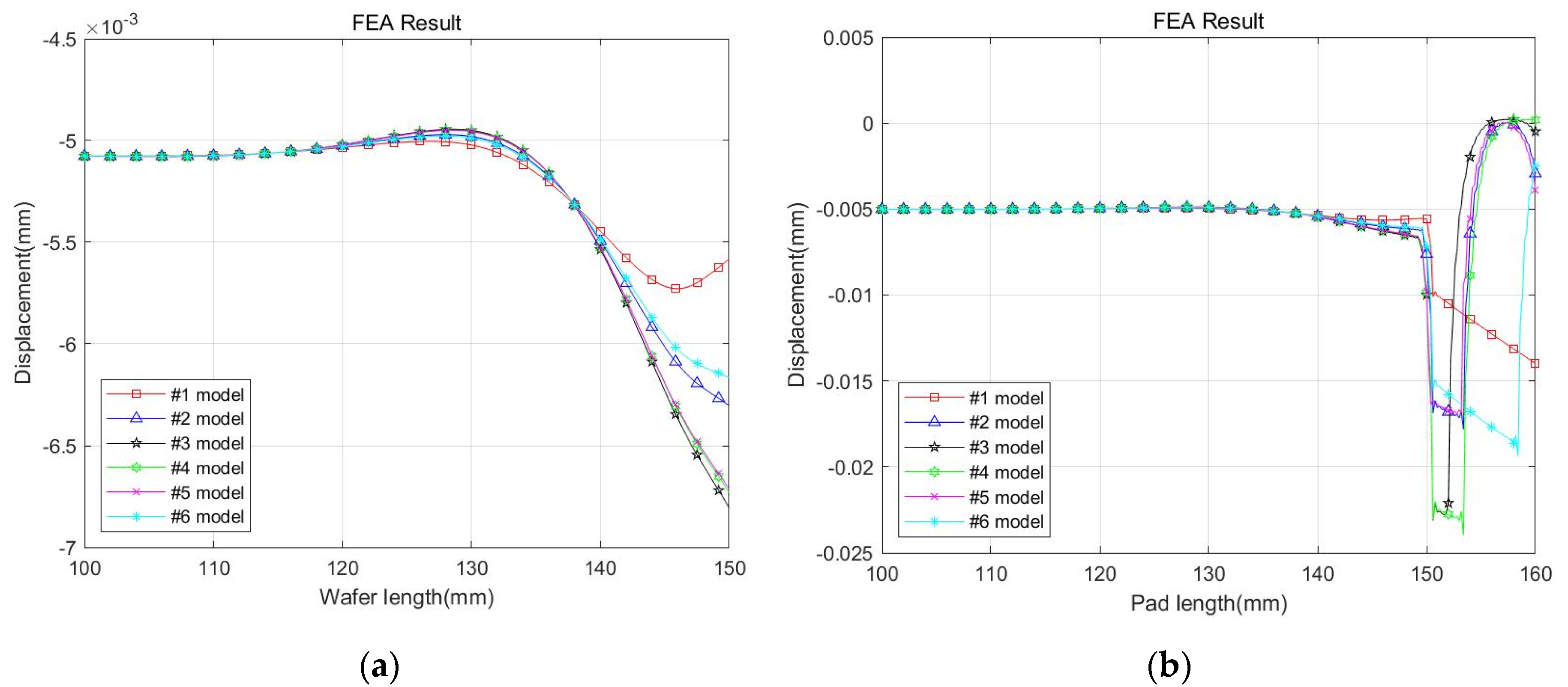
2.4. FEM Verification: Comparison of Test Data

Using the ABAQUS finite element package, the vertical displacements of the upper part of the polishing pad and wafer are calculated. The analysis results are shown in Figure 11 and Figure 12, showing similar behavior to the test result. The analysis result in Figure 11a confirms that model #1 shows the best behavior, as shown in the experimental result in Table 2. Table 6 and Table 7 compare the values at r = 143 mm point where some manufacturers empirically remove the edge of the wafer by 7 mm [16]. As shown in Table 6, it can be confirmed that model #1 has the best performance in both experiments and analysis under the same pressure conditions and that both experimental and analytical results are advantageous in the order #1 > #6 > #2 > #3, #4, #5.
As shown in models #1, #2, and #4 from x = 150 mm to x = 160 mm in Figure 11b, due to the change in adding a groove and widening the width of the groove, the area at the bottom of the retainer ring decreases and transferred pressure applied to the pad increases. As a result, the displacement of the pad located at the bottom of the wafer is increased, and finally, the displacement of the wafer increases, as shown in Figure 11a.
When comparing the results of model #2 and model #5 in Table 6, it can be seen that both the test and analysis results deteriorate due to the reduced inner diameter of model #5. This is presumed to be because the rebound effect increases as the retainer ring gets closer to the wafer. Likewise, when comparing the result of model #2 and model #6, it is estimated that the influence on the wafer edge is reduced when the position of the groove of model #2 is moved from the near side to the far side of the wafer. Table 7 and Figure 12 shows the displacements obtained by changing P1 in model #4. It can be seen that decreasing the pressure at P1 reduces the relative displacement. Since the pressure applied to the retainer ring is the same, it can be observed that the displacement distribution from x = 150 mm to x = 160 mm in Figure 12b is also same. Proper P1 may help to reduce the rebound due to the large pressure on the retainer ring, however, excessive P1 may cause excessive deformation of the wafer itself downward, as shown in Figure 12a. More detailed results for changing P1 will be covered in Section 3.3.
As such, it was confirmed that the FEM model and the existing test results showed a similar trend. Through this, the suggested finite element model was verified indirectly, and in the next section, based on the verified finite element model, in order to improve the non-uniformity of the wafer, the MRR will be predicted as the shape of the retainer ring changes through adding simple machining processes such as machining round shapes or tapering without significantly changing the best model, the current mass production model (model #1).

3. Finite Element Analysis Result: Investigation of the Influence of Pressure Distribution and Shape of Retainer Ring

In this section, based on the basic model (model #1), from an engineering point of view, the influence of the shape changes of the retainer ring is investigated by adding simple machining processes such as machining round sections or tapering without significantly changing the current structure of the retainer ring. In addition, the influence on the load applied to the wafer and retainer ring is investigated.

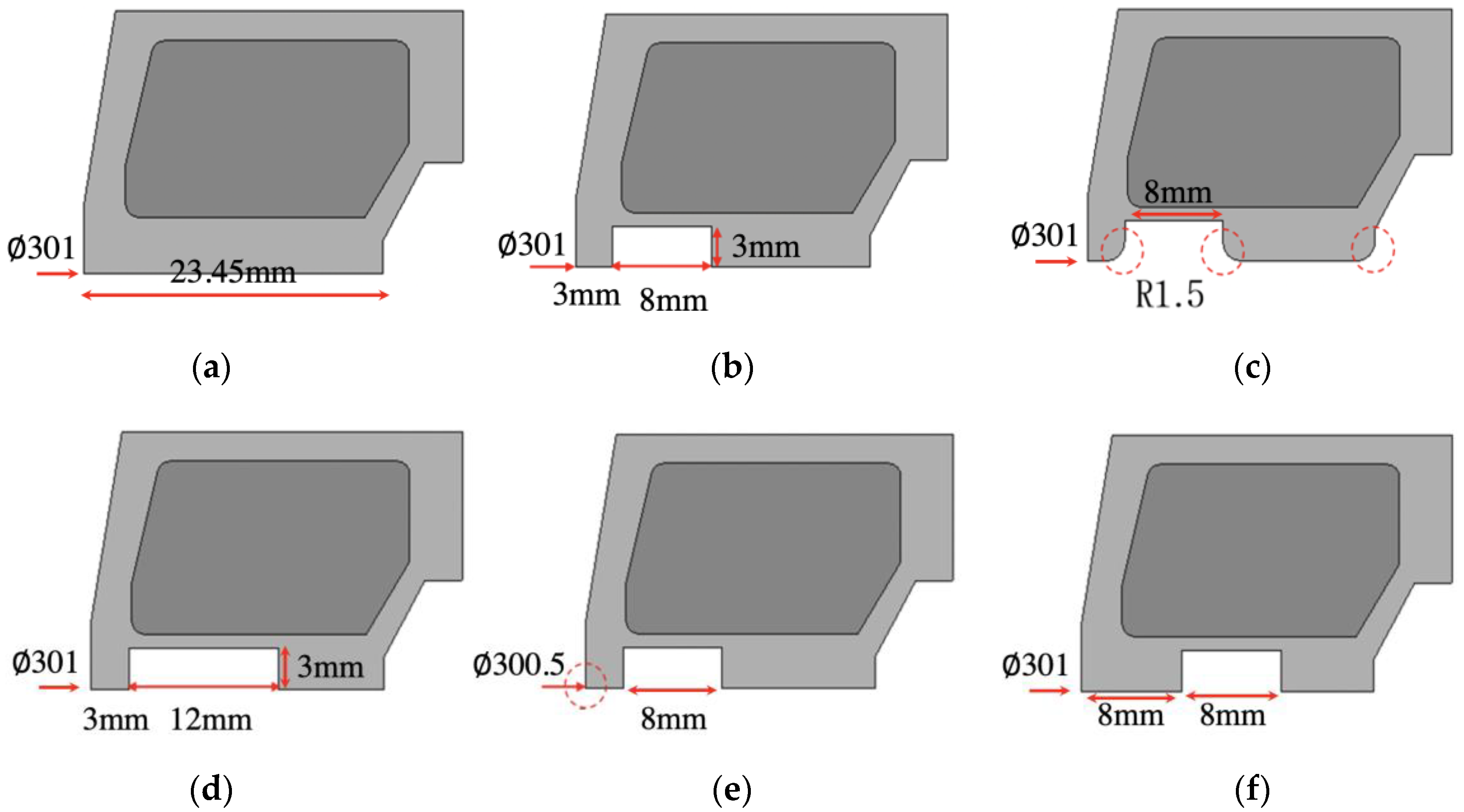
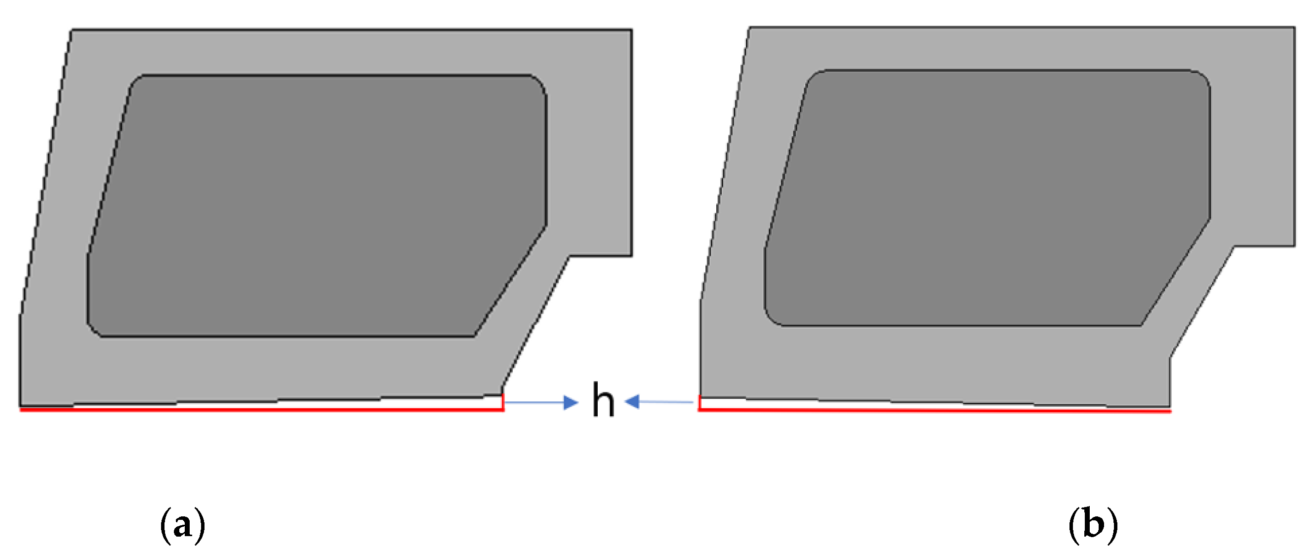
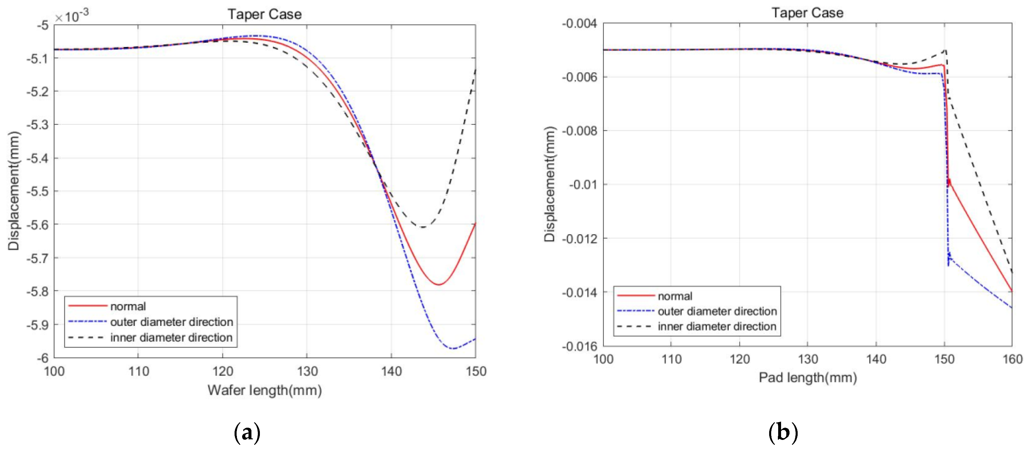
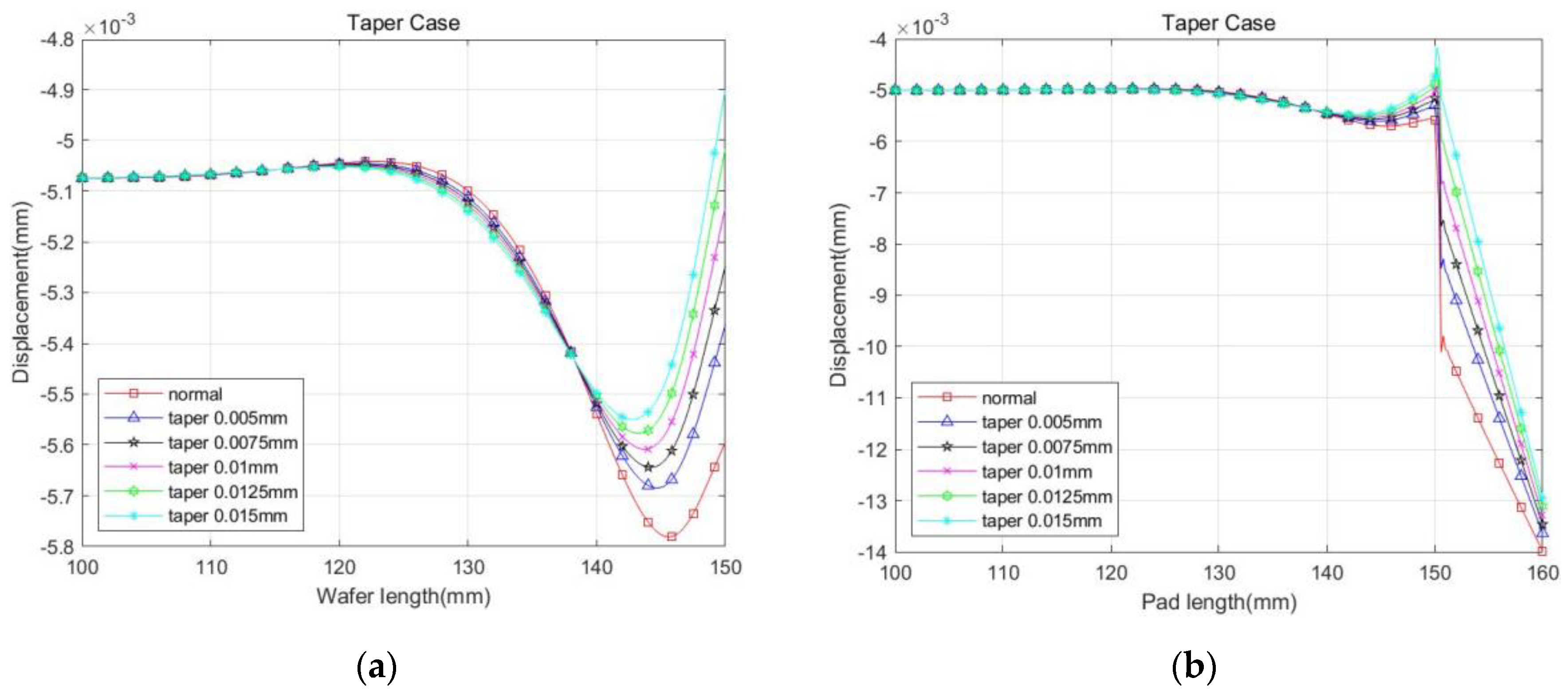
3.1. Investigation of the Impact of the Taper Turning on the Lower Part of the Retainer Ring

The taper turning on the bottom of the retainer ring is applied to investigated the effect on the MRR under the same pressure conditions (i.e., R/P1/P2/P3/P4/P4 = 11.9/9.3/4.4/4.5/4.5/4.7 psi). First, the taper turning (h = 0.01 mm) is given in the direction away from the center of the retainer ring, as shown in Figure 13a, and in the other case, the results are compared by giving it in the other direction, as shown in Figure 13b. As can be seen in Figure 14a, when the taper turning process is given in the direction away from the center of the retainer ring, as the case in Figure 13a, it can be observed that it becomes rather worse than when the taper machining process is not applied. This is because the transmitted pressure from the retainer ring is concentrated near the wafer edge in Figure 14b, resulting in greater non-uniformity within the wafer.
In order to check the optimal amount of the taper as in the case in Figure 13b, the MRR is calculated according to the height, h, of the taper, as shown in Figure 15. As the amount of the taper increases, it can be confirmed that the pressure near the edge of the wafer is released, which is effective in controlling the non-uniformity within the wafer. When h is 0.015 mm, the best MRR results are obtained. That is, as shown in Figure 15a, the maximum relative MRR (MRMRR) in the initial state is 0.7078 × 10⁻³ mm (= 5.7811 × 10⁻³−5.0733 × 10⁻³). When h is 0.015 mm, the MRMRR is 0.4766 × 10⁻³ mm (= 5.5499 × 10⁻³−5.0733 × 10⁻³), which is improved by about 32.7%.

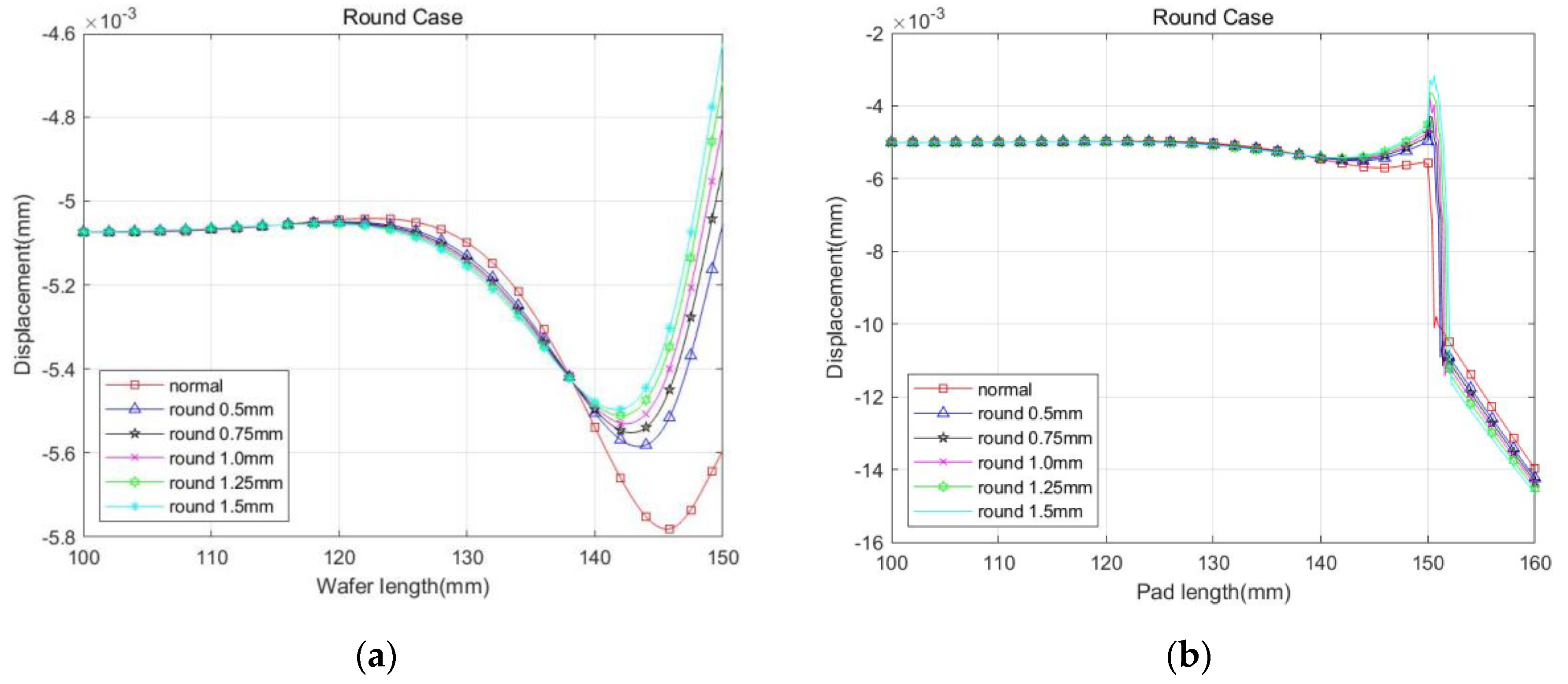
3.2. Investigation of the Influence of Machining Round Corner on the Retainer Ring

As shown in Figure 16, machining inside the round corner of the retainer ring is processed to investigate the effect on the MRR under the same pressure condition (i.e., R/P1/P2/P3/P4/P4 = 11.9/9.3/4.4/4.5/4.5/4.7 psi). As shown in Figure 17, it can be seen that the non-uniformity can be improved by machining the appropriate rounded corner. When r is 1.25 mm, the best MRR results can be obtained. However, when an extreme taper machining process or excessive corner-rounding process is applied, the non-uniformity of the pad’s vertical displacement will be increased too much around d = 150 mm, as can be inferred from the results in Figure 16 and Figure 17. In addition, as the gap between the retainer ring and the wafer is increased by these machining processes, and there is a possibility of the wafer slipping out and being damaged during the CMP process, experimental verification will be required for those cases. However, as can be seen from the analysis results, it is confirmed that the MRR can be improved through an appropriate amount of taper processing and corner-rounding processing. As shown in Figure 17a, the maximum relative MRR (MRMRR) in the initial state is 0.7078 × 10⁻³ mm, and when r is 1.5 mm, the MRMRR is 0.4238 × 10⁻³ mm (= 5.4971 × 10⁻³ − 5.0733 × 10⁻³), which is improved by about 40.1%.

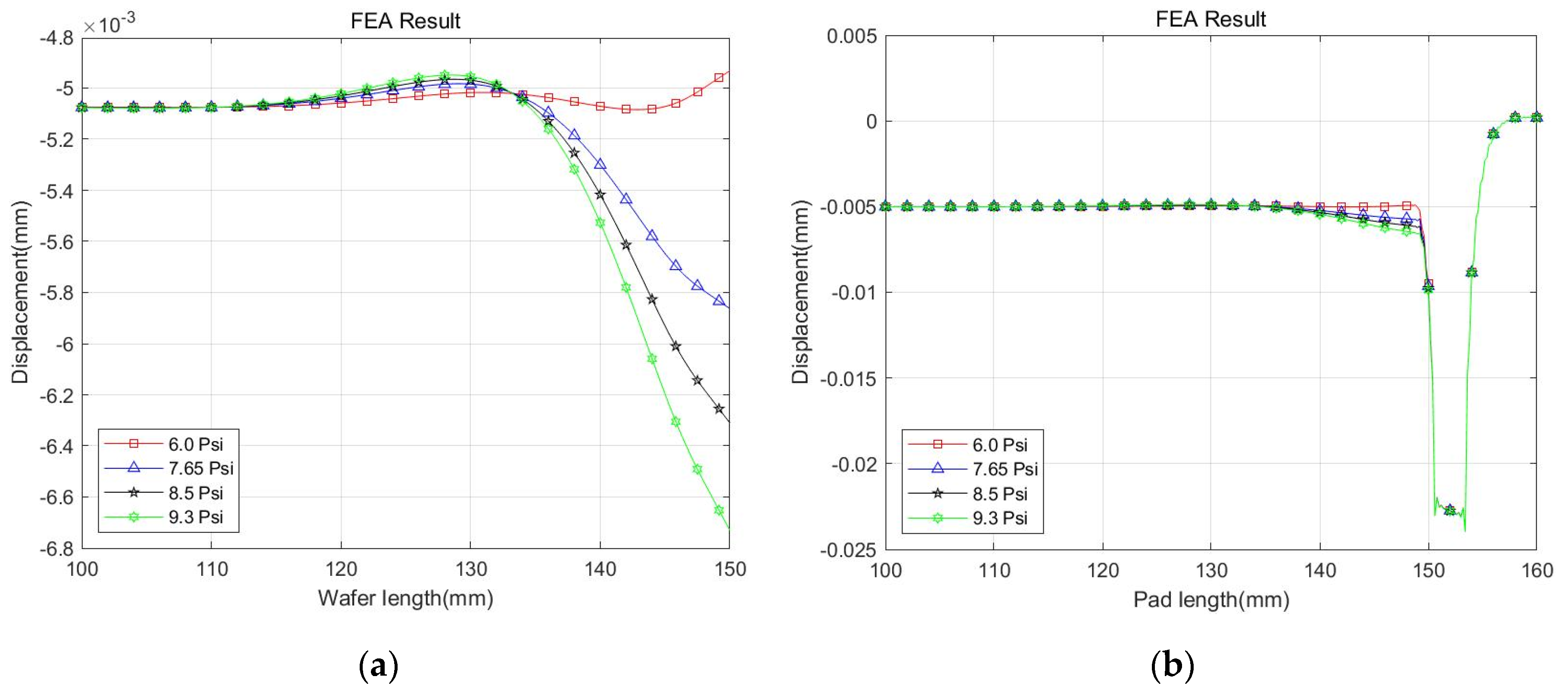
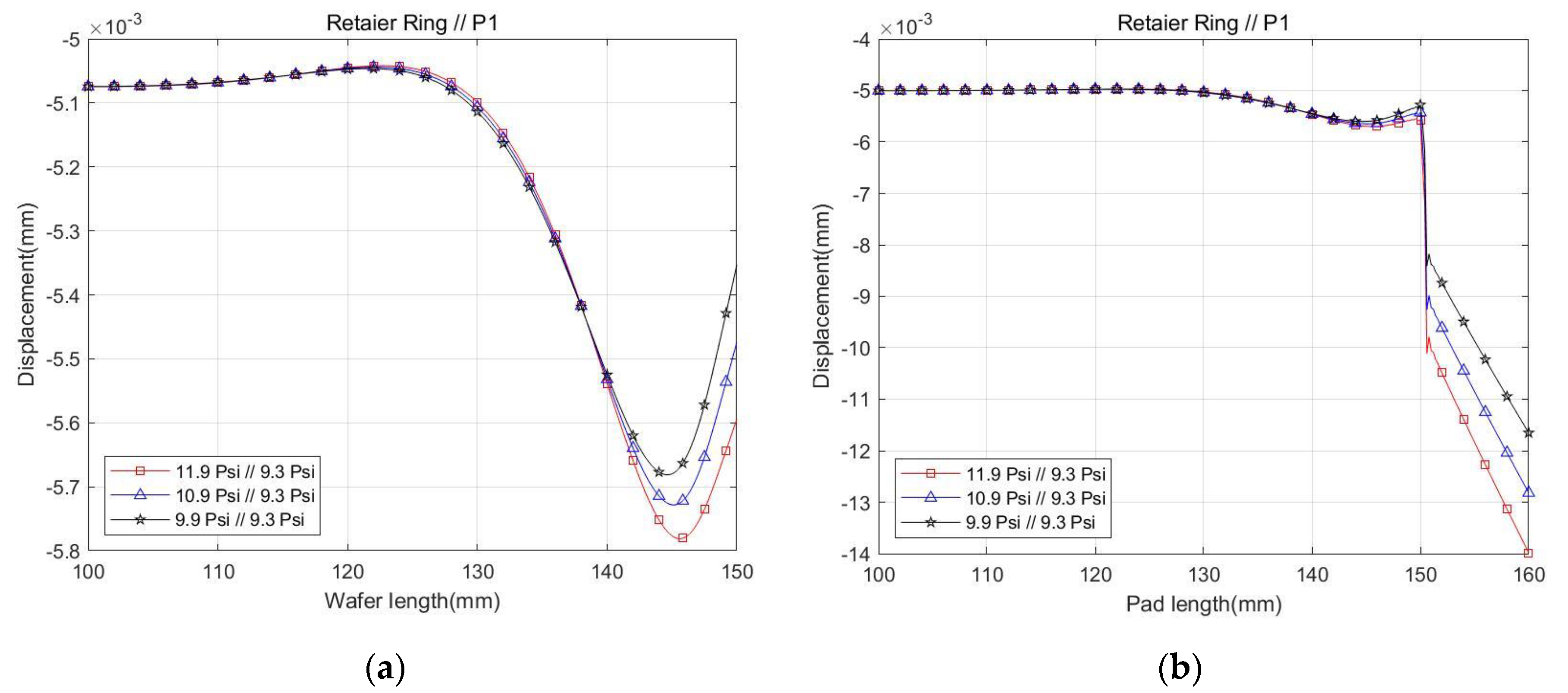
3.3. Investigation of the Influence of P1 Change

In Section 2.2, it was shown experimentally that the non-uniformity could be improved by adjusting P1 (i.e., the applied pressure to zone 1) for model #4. However, if P1 is too low, wafer separation may occur, so in this analysis, the MRR changes for model #1 (the best model) are observed by lowering it to 6.5 psi with a margin of 0.5 psi, where separation did not occur through the previous test (i.e., 6.0 psi). As shown in Figure 18a, it can be seen that lowering P1 generally improves the non-uniformity within the wafer, but if P1 is too low, such as 6.5 psi, as shown in Figure 18a,b, it results in greater non-uniformity at the wafer edge. When P1 is 7.5 psi, the best MRR distribution can be obtained. In the previous two cases, as shown in Figure 14b and Figure 15b, the MRR distribution of the wafer was improved due to the change in the contact pressure distribution (i.e., changes of pad displacement distribution) from the retaining ring (i.e., x = 150–160 mm region in Figure 14b and Figure 15b), but in this case, the displacement of the pad influenced by the retaining (i.e., x = 150–160 mm region) remains the same in Figure 18b and only the MRR of the wafer has changed. As shown in Figure 18a, the MRMRR in the initial state is 0.7078 × 10⁻³ mm, and when P1 is 7.5 psi, the MRMRR is 0.2628 × 10⁻³ mm (= 5.3103 × 10⁻³−5.0733 × 10⁻³), which is improved by about 62.9%.

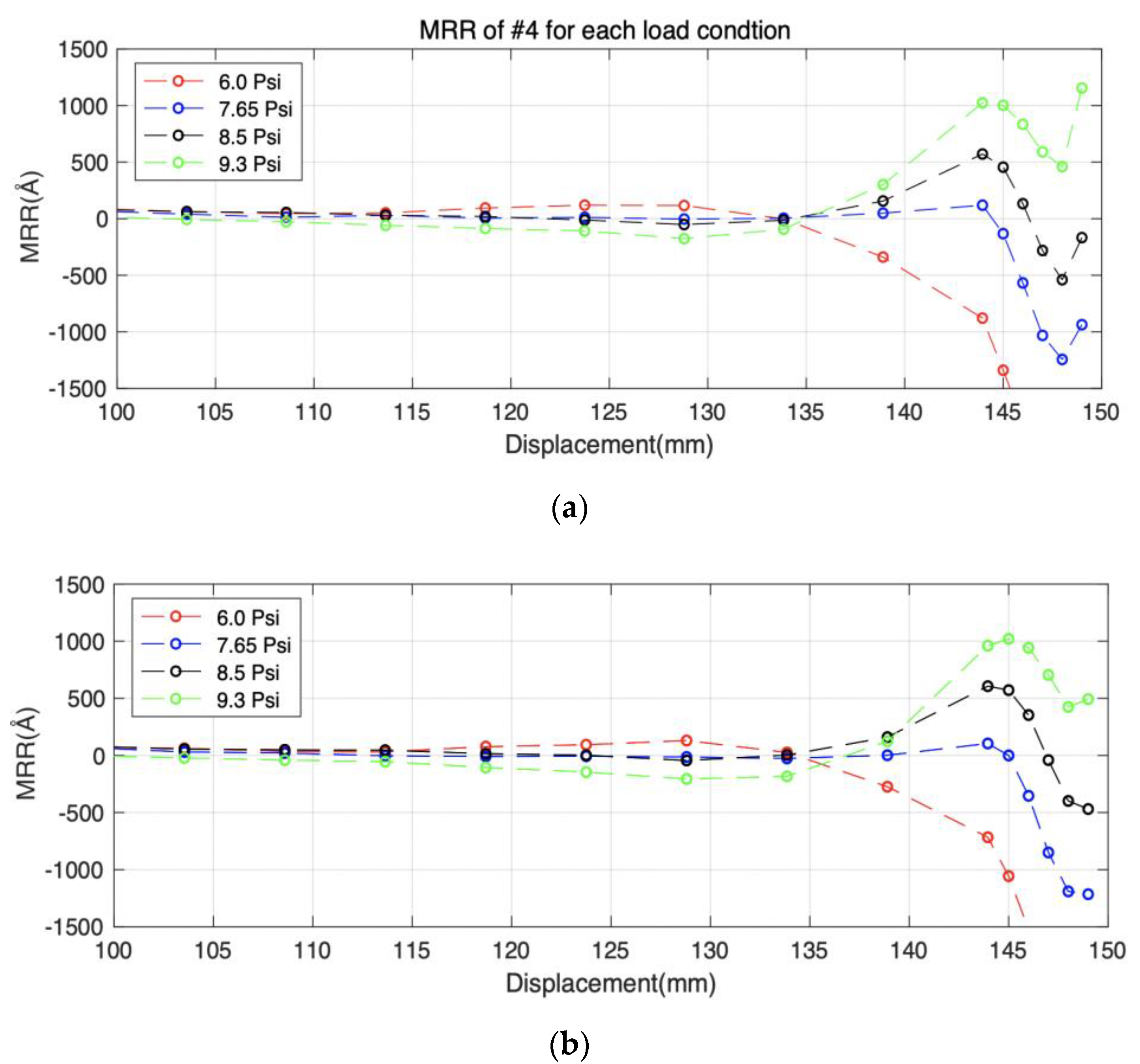
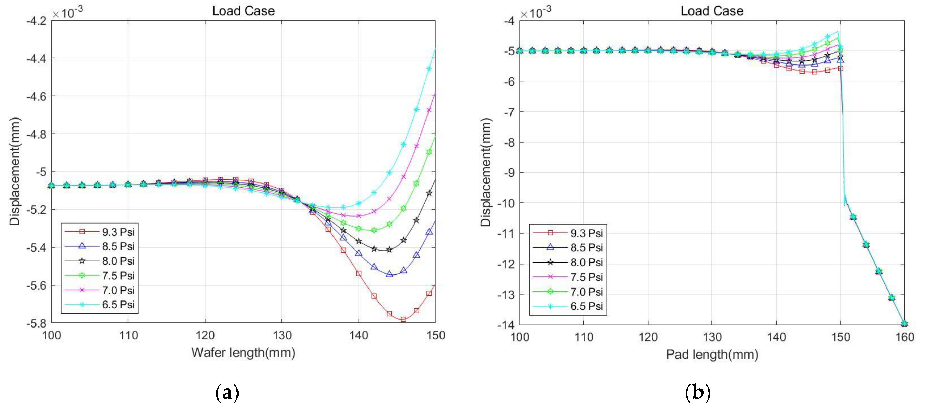
3.4. Investigation of the Influence of the Pressure Change of the Retainer Ring

This time, finite element analysis is performed while gradually decreasing the pressure of the retainer ring from 11.9 psi. If the applied pressure at the retainer ring is smaller than that of P1, it may cause the wafer separation, and since all experimental data were fixed at 11.9 psi, there is not much pressure change from this reference value. As can be seen in Figure 19, when the applied pressure of the retainer ring is reduced, the relative displacement of the pad and wafer is reduced. Therefore, it is estimated that it is effective to reduce the pressure on the retainer ring within the limit that wafer separation does not occur. As shown in Figure 19a, the MRMRR in the initial state is 0.7078 × 10⁻³ mm, and when the applied pressure of the retainer ring is 9.9 psi, the MRMRR is 0.6080 × 10⁻³ mm (= 5.6813 × 10⁻³−5.0733 × 10⁻³), which is improved by about 14.1%.

4. Conclusions

In the CMP process, it is important to reduce the non-uniformity in the wafer to increase the yield of the wafer. In this paper, the effect on the MRR was investigated by adjusting the shape of the metal-inserted retainer ring and the pressure conditions imposed on the wafer edge zone 1 (P1) and the retainer ring. In order to verify the validity of the finite element analysis model, the existing experimental results were used. To improve the MRR distribution in a practical way without significantly changing the existing massive production model, the taper turning process and corner-rounding processes were performed and their effects were investigated. The maximum relative MRR (MRMRR) in the initial state was 0.7078 × 10⁻³ mm. When the height, h, of the taper was 0.015 mm, the best MRR results could be obtained, whereby the maximum relative MRR was 0.4766 × 10⁻³ mm. For machining the rounded corner, when r is 1.25 mm, it provided the best MRR distribution, whereby the maximum relative MRR was 0.4238 × 10⁻³ mm. When the applied pressure of the retainer ring was reduced to 9.9 psi, the maximum relative MRR was 0.6080 × 10⁻³ mm. In addition, when P1 is 7.5 psi, the best MRR distribution could be obtained, and the maximum relative MRR was reduced by about 62.9% to 0.2628 × 10⁻³ mm.
As a future work, a new retainer ring design using topology optimization will be analyzed with the aim of maximizing the wafer yield control by controlling the MRR under given load conditions.

Author Contributions

Conceptualization, J.-H.H. and J.-Y.P.; methodology, C.K.; software, J.-H.H. and J.-Y.P.; validation, J.-H.H. and J.-Y.P.; formal analysis, C.K.; investigation, C.K.; writing—original draft preparation, J.-H.H. and J.-Y.P.; writing—review and editing, C.K.; visualization, J.-Y.P.; supervision, J.-H.H.; funding acquisition, J.-H.H. All authors have read and agreed to the published version of the manuscript.

Funding

This research was partially supported by the National Research Foundation of Korea (NRF) funded by the Ministry of Education (grant no. NRF-2017R1A6A1A03015562 and NRF-2017R1D1A1B-03035405) and the GRRC program of Gyeonggi province [(GRRC-KPU2020-B02), Multi-material Machining Innovative Technology Research Center].

Acknowledgments

We would like to express our deep appreciation to Will be S&T Corp. for providing the MRR test data.

Conflicts of Interest

The authors declare no conflict of interest.

References

  1. Eamajornsiri, S.; Narayannaswami, R.; Chandra, A. Yield Improvement in Wafer Planarization: Modeling and Simulation. J. Manuf. Syst. 2002, 33, 239–247. [Google Scholar]
  2. Preston, F.W. The Theory and Design of Plate Class Polishing Machine. J. Soc. Glass Technol. 1927, 11, 214–256. [Google Scholar]
  3. Xu, Q.; Chen, L.; Yang, F.; Cao, H. Influence of slurry components on copper CMP performance in alkaline slurry. Micoelectr. Eng. 2017, 183–184, 1–11. [Google Scholar] [CrossRef]
  4. Park, I.; Lee, D.; Jeong, S.; Jeong, H. Effect of Temperature on Removal Rate in Cu CMP. J. Korea Soc. Manuf. Process Eng. 2018, 6, 91–97. [Google Scholar] [CrossRef]
  5. Bae, J.; Lee, H.; Park, J.; Nishizawa, H.; Kinoshita, M.; Jeong, H. Effect of Thickness on Removal Rate and Within Wafer Non-Uniformity in Oxide CMP. J. Korea Tribol. Lubr. Eng. 2002, 23, 358–363. [Google Scholar]
  6. Lo, S.; Lin, Y.; Huang, J. Analysis of retaining ring using finite element simulation in chemical polishing process. Int. J. Adv. Manuf. Technol. 2007, 34, 547–555. [Google Scholar] [CrossRef]
  7. Park, Y.; Lee, H.; Park, S.; Jeong, H. Effect on Contact Angle between Retaining Ring and Polishing Pad on Material Removal Uniformity in CMP. Int. J. Precis. Eng. Manuf. 2013, 14, 1513–1518. [Google Scholar] [CrossRef]
  8. Park, S.; An, B.; Lee, J. The Effect of Pressure and Platen Speed on the Material Removal Rate of Sapphire Wafer in the CMP Process. J. Korea Tribol. Lubr. Eng. 2016, 32, 67–71. [Google Scholar]
  9. Fu, G.; Chandra, A. The relationship between wafer surface pressure and wafer backside loading in Chemical Mechanical Polishing. Thin Solid Film. 2005, 474, 217–221. [Google Scholar] [CrossRef]
  10. Kajiwara, J.; Monloney, G.; Wang, H.; Harsen, A.; Reyes, A. System and Method for Pneumatic Diaphragm CMP Head having Separate Retaining Ring and Multi-Region Wafer Pressure Control. U.S. Patent 6,506,105 B1, 14 January 2003. [Google Scholar]
  11. Wang, T.; Lu, X.; Zhao, D.; He, Y. Contact stress non-uniformity of wafer surface for multi-zone chemical mechanical polishing process. Sci. China Technol. Sci. 2011, 56, 1974–1979. [Google Scholar] [CrossRef]
  12. Wang, T.; Lu, X. Numerical and experimental investigation on Multi-zone chemical mechanical planarization. Microelectron. Eng. 2001, 88, 3327–3332. [Google Scholar] [CrossRef]
  13. Kalenian, W.; Speigel, L. CMP Retaining Ring with Soft Retaining Ring Insert. U.S. Patent 9,193,030 B2, 24 November 2015. [Google Scholar]
  14. Park, K.; Park, D. Effect of Insert Material of the Performance of Wafer Polishing Finish in Oxide CMP. J. Korea Manuf. Process Eng. 2019, 18, 44–50. [Google Scholar]
  15. Park, K.; Kim, E.; Park, D. Effect of CMP Retaining ring Material on the Performance of Wafer Polishing. J. Korea Manuf. Process Eng. 2020, 19, 22–28. [Google Scholar] [CrossRef]
  16. Han, J.; Choi, J.; Kim, K. A Study on the Shape of Two-Piece Type Retainer Rings to Increase Usable Wafer Area. J. Korea Inst. Ind. Eng. 2020, 46, 55–63. [Google Scholar]
  17. Lu, X.; Khonsari, M.; Gelinck, E. The Stribeck curce: Experimental results and theoretical prediction. J. Tribol. 2006, 128, 789–794. [Google Scholar] [CrossRef]
Figure 1. Schematic diagram of chemical mechanical polishing (CMP) process.
Applsci 10 08362 g001
Figure 2. Shape of retainer ring: (a) top view, (b) bottom view, (c) cross section.
Applsci 10 08362 g002
Figure 3. Cross section information of test samples: (a) model #1, (b) model #2, (c) model #3, (d) model #4, (e) model #5, (f) model #6.
Applsci 10 08362 g003
Figure 4. Experimental results of six samples (relative material removal rate (MRR)): (a) left-hand side, (b) right-had side.
Applsci 10 08362 g004
Figure 5. Experimental result of model #4 for change in P1: (a) left-hand side, (b) right-had side.
Applsci 10 08362 g005
Figure 6. Modal experimental setup.
Applsci 10 08362 g006
Figure 7. Three-dimensional model for finite element model.
Applsci 10 08362 g007
Figure 8. Finite element analysis data extraction in the circumferential direction.
Applsci 10 08362 g008
Figure 9. Schematic diagram of 2D axisymmetric model.
Applsci 10 08362 g009
Figure 10. Finite element analysis result of full 3D model and 2D axisymmetric model.
Applsci 10 08362 g010
Figure 11. Finite element analysis results of all models: (a) displacement of wafer, (b) displacement of pad.
Applsci 10 08362 g011
Figure 12. Finite element analysis results of model #4 for change in P1: (a) displacement of pad, (b) displacement of pad.
Applsci 10 08362 g012
Figure 13. Taper direction for each model: (a) outer diameter direction, (b) inner diameter direction.
Applsci 10 08362 g013
Figure 14. Finite element analysis result for taper direction: (a) displacement of wafer, (b) displacement of pad.
Applsci 10 08362 g014
Figure 15. Finite element analysis result according to each taper amount: (a) displacement of wafer, (b) displacement of pad.
Applsci 10 08362 g015
Figure 16. Cross section of inner corner-rounded model.
Applsci 10 08362 g016
Figure 17. Finite element analysis result of corner-rounded case: (a) displacement of wafer, (b) displacement of pad.
Applsci 10 08362 g017
Figure 18. Finite element analysis result for change in P1: (a) displacement of wafer, (b) displacement of pad.
Applsci 10 08362 g018
Figure 19. Finite element analysis result for change retainer ring pressure: (a) displacement of wafer, (b) displacement of pad.
Applsci 10 08362 g019
Table 1. Applied pressure distribution on wafer.
Distance from Wafer Center [mm]Zone 1 (P1)Zone 2 (P2)Zone 3 (P3)Zone 4 (P4)Zone 5 (P5)
145–150128–145100–12840–1000–40
Table 2. Experimental results of six samples.
Unit: Å#1#2#3#4#5#6
Maximum relative MRR
[averaged]
893/182
551/179
[450]
1083/915
1102/954
[1014]
1097/1092
158/1079
[1107]
1148/1027
1133/1118
[1107]
1215/825
1554/1533
[1282]
583/585
494/535
[549]
Relative MRR@7mm
[averaged]
−5/14
195/157
[90]
880/786
964/776
[852]
951/883
1002/887
[931]
881/810
966/892
[887]
1053/661
1344/1255
[1078]
446/470
452/445
[453]
Table 3. MRR result of model #4 for each load condition (R/P2/P3/P4/P4 = 11.9/4.4/4.5/4.5/4.7 psi).
P1 [psi]9.38.57.656.0
Maximum relative MRR
[averaged]
1148/1027
1133/1118
[1107]
572/606
[589]
−1244/−1215
[−1230]
−2175/−2121
[−2148]
Relative MRR@7mm
[averaged]
881/810
966/892
[887]
502/514
[508]
106/85
[96]
−779/−631
[−705]
Table 4. Material properties.
Elastic Modulus (MPa)Density (kg/m3)Poisson’s Ratio
Wafer10,00023290.22
Retainer ring (Polyether ether ketone)293511740.39
Retainer ring (Inner metal ring)70,08060200.32
Pad20350.1
Platen190,00078500.3
Table 5. Element types and number of elements for finite element model.
WaferRetainer Ring (Model #1)PadPlaten
3D modelNo. of node #
No. of element
Element type
Approx. size
79,456
39,463
C3D8R
1.5 mm
422,558
244,576
C3D10/C3D8R
2 mm
82,622
40,991
C3D8R
4 mm
13,416
27,198
C3D8R
7 mm
2D axisymmetric modelNo. of node #
No. of element
Element type
Approx. size
3780
3020
CAX4R
0.2 mm
15654
15324
CAX4R
0.2 mm
34527
32480
CAX4R
0.2 mm
4477
4060
CAX4R
1 mm
Table 6. Summary of test and finite element analysis result of all models.
ModelTest Result
Averaged Relative MRR
at r = 143 mm (Å)
Finite Element Analysis Result
Pad Relative Displacement
at r = 143 mm (10−6 mm)
Finite Element Analysis Result
Wafer Relative Displacement
at r = 143 mm (10−6 mm)
#190539547
#2852714724
#3931846857
#4887823835
#51078822833
#6453679689
Table 7. Summary of test and finite element analysis result of model #4 for change in P1.
P1Test Result
Averaged Relative MRR
at r = 143 mm (Å)
Finite Element Analysis Result
Pad Relative Displacement
at r = 143 mm (10−6 mm)
FEA Result
Wafer Relative Displacement
at r = 143 mm (10−6 mm)
6.0 psi−705−6−7
7.65 psi96416421
8.5 psi508626634
9.3 psi887823835
Publisher’s Note: MDPI stays neutral with regard to jurisdictional claims in published maps and institutional affiliations.

