Article

Common-Mode Voltage Analysis and Reduction for the Quasi-Z-Source Inverter with a Split Inductor

1
Department of Energy Technology, Aalborg University, 9220 Aalborg, Denmark
2
Department of Electrical Power Engineering and Mechatronics, Tallinn University of Technology, 19086 Tallinn, Estonia
*
Author to whom correspondence should be addressed.
Appl. Sci. 2020, 10(23), 8713; https://doi.org/10.3390/app10238713
Submission received: 5 November 2020 / Revised: 28 November 2020 / Accepted: 1 December 2020 / Published: 4 December 2020
(This article belongs to the Special Issue Advancing Grid-Connected Renewable Generation Systems 2019)

Abstract

:
In transformerless grid-connected photovoltaic (PV) systems, leakage currents should be properly addressed. The voltage fluctuations between the neutral point of the grid and the PV array, i.e., common-mode voltage (CMV), will affect the value of the leakage currents. Therefore, the leakage currents can be attenuated through proper control of the CMV. The CMV depends on the converter topology and the modulation strategy. For the quasi-Z-source inverter (qZSI), the amplitude of the high-frequency components in the CMV increases due to the extra shoot-through (ST) state. The CMV reduction strategies for the conventional voltage source inverter (VSI) should be modified when applied to the qZSI. In this paper, an input-split-inductor qZSI is introduced to reduce the CMV, in which all the CMV reduction strategies for the VSI can be used directly with appropriate ST state insertion. Moreover, the proposed method can be extended to impedance source converters with a similar structure. Simulations and experimental tests demonstrate the effectiveness of the proposed strategy for the qZSI in terms of CMV reduction.

1. Introduction

The interest in renewable power generation systems has been increasing with no signs of slowing down in recent years worldwide. The photovoltaic (PV) arrays are particularly attractive as a renewable source for distributed generation with the advantages of relatively small size, noiseless operation and simple installations [1]. Due to the low-voltage and intermittent output characteristics of the PV arrays, power electronics are essential interfaces to deliver solar energy to the grid or residential applications with boosting capability. The conventional topologies for PV applications either employ a high-frequency or a low-frequency transformer for galvanic isolation between the PV arrays and the grid, which results in higher cost, larger volume and lower efficiency. Recently, the transformerless alternatives have been receiving more and more attention by addressing the aforementioned issues. However, the leakage current may appear due to the PV array parasitic capacitance to the ground. Leakage currents bring many concerns, e.g., electromagnetic interference issues, fault activation of detector circuits and harmonic currents [2,3,4]. Therefore, the leakage current should be suppressed within a certain level according to the standards like the IEC 62109-2 [5].
The fluctuations between the grid and PV array, i.e., common-mode voltage (CMV), will induce large leakage currents flowing through the parasitic capacitors in a transformerless PV system [6,7]. To tackle the leakage current issue, various topologies and modulation methods have been proposed [8,9,10]. The basic principle of the topology modification is to introduce new paths to isolate the PV array from the grid, e.g., a highly efficient and reliable inverter concept (HERIC). The CMV amplitude depends on the choice of the switching vectors in the same topology. Hence, there are various pulse width modulation (PWM) methods that can reduce the CMV, such as discontinuous pulse width modulation (DPWM), active zero state pulse width modulation (AZSPWM), near state pulse width modulation (NSPWM) and remote state pulse width modulation (RSPWM) [11,12,13]. While the conventional PWM methods make the most use of all the vector states, the modified PWM methods can reduce the CMV with active vector states and partial zero vector states to generate the output. DPWM adopts all the active vector states and partial zero vectors to eliminate the CMV. RSPWM uses the active vector states, e.g., odd vectors or even vectors, which lead to the same CMV amplitude. NSPWM adopts the adjacent active vector states to generate the output that meets the reference requirement. Furthermore, the CMV can also be alleviated by changing the traditional control schemes [14,15,16,17,18,19].
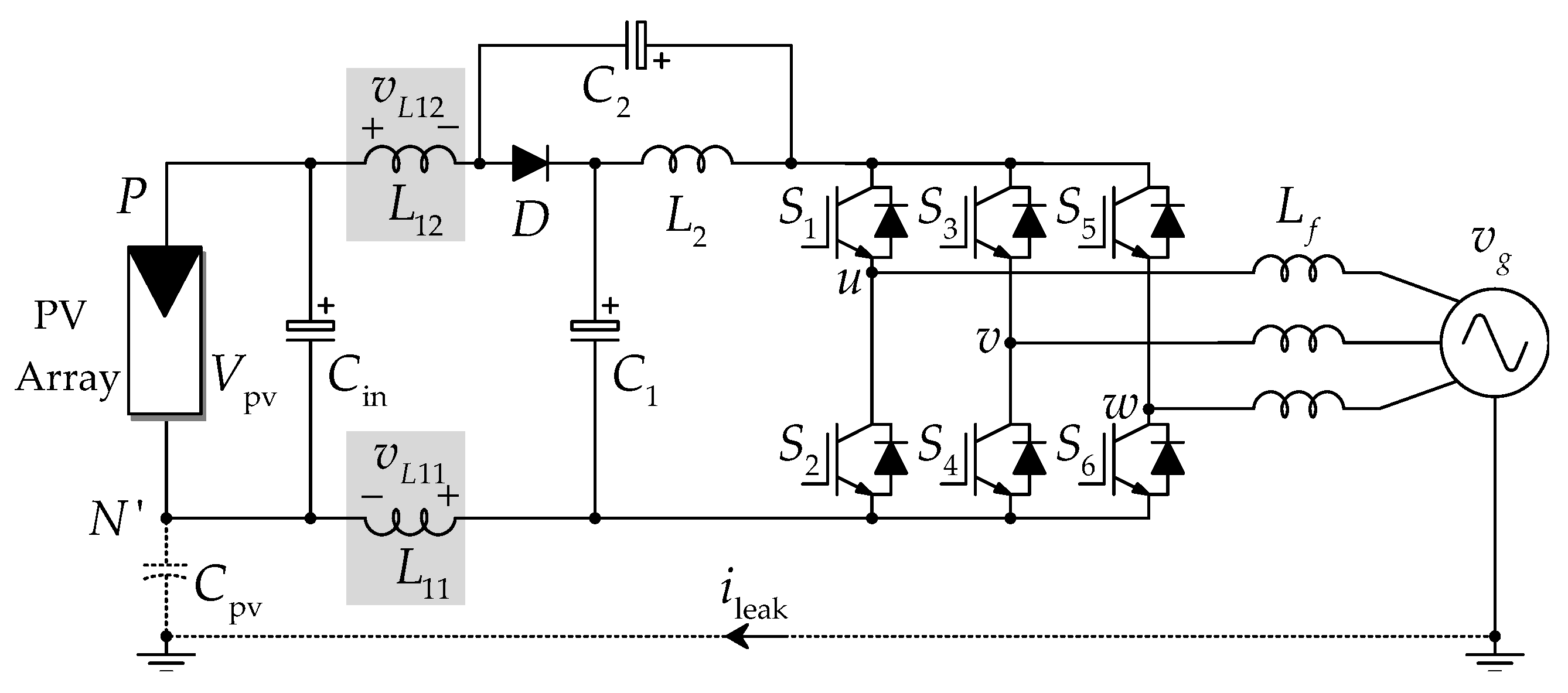
In terms of topology, the quasi-Z-source inverter (qZSI) has been considered as an alternative to the conventional two-stage two-level inverter [20,21,22,23,24]. The qZSI can operate as a single-stage converter by utilizing the shoot-through (ST) state. Due to its advantages, like a continuous input current and a common ground point between the input and the DC-link, the qZSI can be an attractive candidate for renewable applications with a wide input range. A typical three-phase grid-connected qZSI is presented in Figure 1. As a transformerless inverter, the CMV fluctuations in the qZSI can also lead to large leakage currents. The high-frequency components in the CMV of the qZSI are much larger than those in the conventional two-stage transformerless inverter when the ST states were adopted [25]. When the prior-state-of-the-art CMV reduction strategies for the conventional voltage source inverter (VSI) are applied to the qZSI, the high-frequency components are still large, which results from the ST state. To address this issue, various strategies have been proposed. In [26], the CMV in the qZSI with different modulation methods was analysed in detail. A modified PWM method, which only utilizes odd vectors and the ST vector, was proposed in [27]. However, the maximum modulation index decreased dramatically. To tackle the limited modulation index, the three-phase four-leg qZSI was proposed in [28,29] with an extra phase leg. In [30], a recovery diode was adopted in the negative side of the PV array to cut off the power flow of the CMV when the ZSI is operating in the ST state. However, the ZSI will be disconnected from the PV array, which results in discontinuous input conditions. To further take advantage of the qZSI system, it is essential to deal with the high-frequency components in the CMV that result from the ST state. Meanwhile, further explorations are needed to make the CMV reduction strategies for the conventional VSI also available for the qZSI system.
In light of the above, this paper explores the CMV reduction strategies for the qZSI system based on the methods for the conventional VSI without introducing additional circuits. By splitting the input inductor into two parts, which maintains the total inductance, the high-frequency components due to the ST state can be reduced to some extent. With the inductor-splitting method, all the conventional CMV reduction strategies for the VSI can be used for the qZSI with appropriate ST state insertion. More importantly, the proposed split-inductor qZSI shows the same operating features as the original qZSI. The rest of this paper is organized as follows. The CMV of the qZSI is derived in Section 2, in which the effect of the ST state on the CMV of the qZSI is discussed. The CMV reduction strategies for the conventional VSI are presented in Section 3 in detail. The CMV of the proposed input split-inductor qZSI is explored when the conventional CMV reduction strategies are used in Section 4. Simulations and experimental tests demonstrate the effectiveness of the proposed strategy for the qZSI in terms of CMV reduction in Section 5. Finally, concluding remarks are given in Section 6.

2. CMV Analysis in Different Operational States for the qZSI

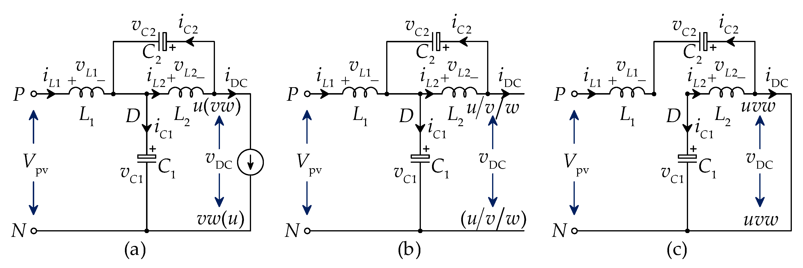
As shown in Figure 1, the qZSI consists of two identical inductors ( L 1 , L 2 ), two identical capacitors ( C 1 , C 2 ), a diode (D) and a conventional VSI. There are three different operation states in the qZSI system: the active state, the null state and the ST state. Figure 2 illustrates the equivalent circuits of the qZSI in the three states [31,32]. As a transformerless inverter, leakage currents may appear, as previously mentioned. The leakage current is related to the CMV, which is defined as the average value of the voltages between the outputs (as u, v, w) and the common reference in a three-phase inverter. In the qZSI, the negative terminal (marked as N) of the input source v in is the common reference. Thus, the CMV for the qZSI is obtained as [33]:
v cmv = v u N + v v N + v w N 3
where v cmv is the CMV and v i N ( i = u , v , w ) is the voltage from point “i” to the negative terminal N.
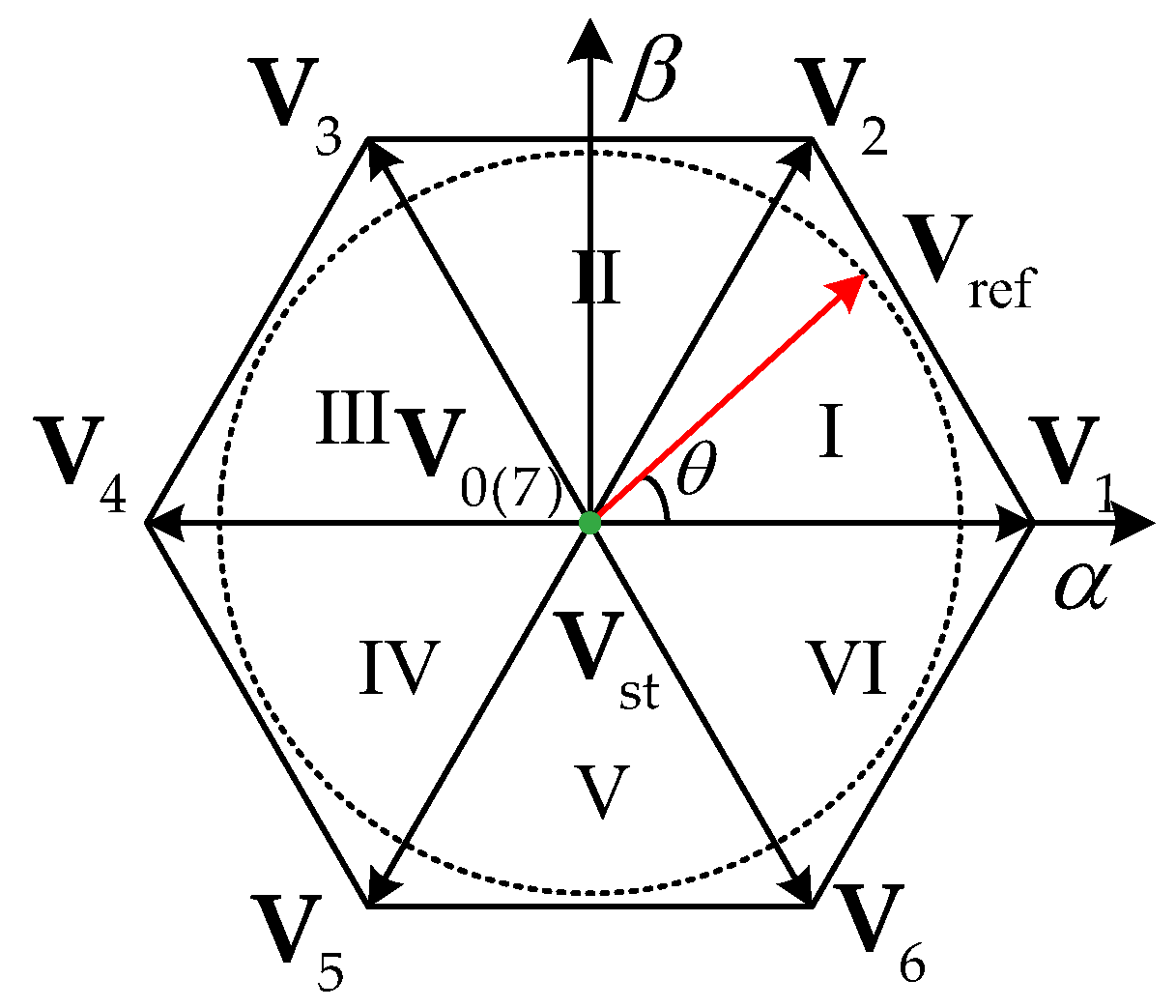
The space-vector PWM (SVPWM) has eight possible combinations of the switch vectors in the conventional VSI: six active vectors ( V 1 , V 2 , V 3 , V 4 , V 5 , V 6 ) and two zero vectors ( V 0 , V 7 ), as shown in Figure 3. θ in Figure 3 is the angle of the output reference V ref . In addition to the eight traditional switching states, the qZSI has seven ST zero states ( V s t u , V s t v , V s t w , V s t u v , V s t u w , V s t v w , V s t u v w ). The CMV can be calculated according to the equivalent circuits in Figure 2 as follows with the corresponding switching states.

2.1. CMV during the Active State

Figure 2a shows the equivalent circuit of the qZSI during the active state. In this state, the diode is conducting. The input voltage and inductors provide energy to the inverter side and charge the capacitors simultaneously. Applying (1) in the equivalent circuit in Figure 2a, the CMV in the active state can be calculated with odd vectors or even vectors as:
v cmv o d d = v C 1 + v C 2 + 0 + 0 3 = v C 1 + v C 2 3
in which v cmv o d d is the same value for all odd active vectors ( V 1 , V 3 , V 5 ). This is because during these vectors, only one phase is connected to the impedance network through the upper switch and two phases are connected through the lower switches. The CMV with the even vectors is obtained as:
v cmv e v e n = 2 ( v C 1 + v C 2 ) + 0 3 = 2 ( v C 1 + v C 2 ) 3
where v cmv e v e n represents the same value for all even active vectors ( V 2 , V 4 , V 6 ). Similarly, in this case, two phases are connected to the qZSn through the upper switches, and only one phase is connected through the lower switch.

2.2. CMV during the Null State

Figure 2b shows the equivalent circuit of the qZSI during the null state. In this state, the diode is also conducting. The output voltage of the inverter is zero, and the impedance-source network is disconnected from the inverter with no energy being transferred from the impedance-source network to the inverter. Meanwhile, the input source and the inductors are still charging the capacitors. Applying (1) to the equivalent circuit in Figure 2b, the CMV can be calculated as:
v cmv 0 = 0 + 0 + 0 3 = 0
v cmv 7 = 3 ( v C 1 + v C 2 ) 3 = v C 1 + v C 2
with v cmv 0 and v cmv 7 being the CMV values for zero vectors V 0 and V 7 , respectively. During the zero vector V 0 , all three phases are connected to the qZSn through the lower switches. While this works with the zero vector V 7 state, all three phases are connected to the qZSn through the upper switches.

2.3. CMV during the Shoot-Through State

Figure 2c shows the equivalent circuit of the qZSI during the ST state. In this case, the diode is reverse-biased and the capacitors transfer energy to the inductors. According to (1) and the equivalent circuit in Figure 2c, the CMV can be obtained as:
v cmv s t = 0 + 0 + 0 3 = 0
where v cmv s t is the CMV for all the ST vectors. During the ST state, all three phases are connected to the common reference.
During the ST state, the DC-link voltage is zero. However, during the active state and null state, the DC-link voltage reaches its peak value, which is equal to the sum of the two capacitor voltages in the qZSn. The relationship between the peak DC-link voltage and the two capacitor voltages can be described as:
v DC = v C 1 + v C 2
Assuming that the peak DC-link voltage and the capacitor voltages are constant during the operation and D is defined as the ST duty ratio in a switching cycle, in steady-state, the voltages of the two capacitors can be obtained as:
V C 1 = ( 1 D ) V DC
V C 2 = D V DC
The CMV values in different states can be obtained according to (7)–(9). Table 1 shows the switching vectors and the relevant CMV values. The CMV values in the qZSI are not constant in a switching cycle with the utilization of different vectors, as shown in Table 1. Thus, the CMV values vary depending on the modulation methods. The CMV fluctuation can lead to large leakage currents when the qZSI is applied to the PV system.

3. CMV Reduction Strategies for the VSI

Although the PV system with isolation between the PV arrays and the grid side can avoid the leakage current issue, the transformerless PV system is more attractive with higher efficiency and lower weight considering the installation cost. However, the CMV of the transformerless system should be limited to decrease the leakage current. The common-mode filter at the output side can realize CMV reduction, but the system size and cost are further increased. The amplitude of the CMV is related to the operation states, as shown in Table 1, making the modulation strategies available for CMV reduction. By appropriately locating the sequence of the operation states in a switching cycle, the fluctuation of the CMV in the VSI can be limited. Many modulation strategies for CMV reduction have been proposed for the conventional VSI, e.g., DPWM, AZSPWM, NSPWM and RSPWM, as shown in Figure 4. The conventional CMV reduction strategies are discussed in the following with exemplified switching patterns and CMV in a switching cycle.
The conventional SVPWM uses all the vectors, as shown in Figure 3, while the CMV reduction strategies for the VSI adopt partial switching vectors to reduce the CMV. Figure 4a shows the switching signals for S 1 , S 3 and S 5 in the VSI (see Figure 1) and the corresponding CMV values. In the conventional VSI, the switches in the same leg, e.g., S 1 and S 2 in Figure 1, are complementary. In Sector 1, the DPWM uses two adjacent active states V 1 , V 2 and a zero vector V 7 , where the zero vector V 0 will not be included. The CMV, with the DPWM, varies from V DC 3 to V DC , for which the amplitude is shown in Table 1. All the active vector states, i.e., V 1 V 6 , are used in the DPWM, which makes the DC-link voltage utilization identical to the conventional SVPWM method. Figure 4b shows the switching signals and corresponding CMV values when AZSPWM is used. S 3 and S 6 are used to create an output state that is the same as the zero state, while the zero vectors V 0 and V 7 are eliminated to reduce the CMV amplitude. AZSPWM adopts only the active vector states, making the CMV amplitude vary between V DC 3 and 2 V DC 3 . More importantly, the maximum DC-link utilization ratio is the same as that with DPWM. Referring to Table 1, a constant CMV can be obtained when only odd or even switching patterns are used, i.e., NSPWM, as shown in Figure 4c. The CMV is V DC 3 with only odd vectors, i.e., V 1 , V 3 and V 5 , and 2 V DC 3 with only even vectors, i.e., V 2 , V 4 and V 6 . However, the maximum DC-link voltage utilization is reduced to 0.67, which is much smaller than that when the SVPWM is adopted. As shown in Figure 4d, NSPWM adopts three active vector states that are close to the output reference without using any zero vectors. There are two kinds of switching patterns with the NSPWM in the same space sector. For example, in Sector 1, the switching vectors are V 1 , V 2 , V 6 when the output angular θ meets 0 θ < π / 6 , while the switching vectors are V 1 , V 2 , V 3 when π / 6 θ π / 3 . NSPWM also uses only active vector states to reduce the CMV and maintain the same maximum DC-link voltage utilization ratio. However, when the ST vector state is inserted, the conventional CMV reduction strategies for the VSI are no longer available for the qZSI. Thus, further work should be done to tackle this issue, making the conventional CMV reduction methods appropriate for the qZSI system.

4. Modified qZSI for CMV Reduction

The qZSI can achieve the boost capability by utilizing the ST vectors. The introduction of the ST vectors will also change the CMV. According to Table 1, the CMV is zero when the ST vector state is adopted, introducing high-frequency harmonics. Thus, an input-split-inductor qZSI is adopted to reduce the CMV when the ST vector state is utilized in the conventional CMV reduction strategies. According to the vectors, the average CMV value during the non-ST state and the CMV during the ST state is applied, which can reduce the high-frequency components in the CMV. The CMV reduction in the qZSI can be achieved in the following.
According to Figure 2, the voltage of the inductor L 1 during the non-ST state can be obtained as
v L 1 = D V DC
while the voltage of the inductor L 1 during the ST state can be described as
v L 1 = ( 1 D ) V DC
The CMV and the inductor voltage in the qZSI are presented in Figure 5, in which v cmv is the CMV, v cmv _ avg is the average CMV during the non-ST state when DPWM, AZPWM, RSPWM and NSPWM are used. The average CMV during the non-ST state can be obtained as
v cmv _ avg = 0 · t z e r o _ 0 + V DC 3 · t o d d + 2 V DC 3 · t e v e n + V DC · t z e r o _ 7 t z e r o + t o d d + t e v e n
in which t o d d is the time interval of all the odd vector states, i.e., V 1 , V 3 and V 5 , t e v e n is the time interval of all the even vector states, i.e., V 2 , V 4 and V 6 , t z e r o _ 0 is the time interval of the zero vector state V 0 , t z e r o _ 7 is the time interval of the zero vector state V 7 and t z e r o is the sum of t z e r o _ 0 and t z e r o _ 7 .
As observed in Figure 5, the voltage of the inductor L 1 is positive with its maximum value being ( 1 D ) V DC during the ST state when v cm is zero. Meanwhile, the voltage of the inductor L 1 is negative with its minimum value being D V DC during the ST state when v cm _ avg is positive. According to the phenomenon seen from the CMV and the inductor voltage, the input inductor voltage can be used to compensate for the CMV by splitting the inductor and maintaining the same total inductance. The inductor L 1 can be divided into L 11 and L 12 , as shown in Figure 6. The proportional relationship among L 1 , L 11 and L 12 can be obtained as
L 11 = x L 1 L 12 = ( 1 x ) L 1
where x is a coefficient that is used to describe the ratio of the split inductor, and then:
v L 11 = x v L 1 v L 12 = ( 1 x ) v L 1
in which v L 11 and v L 12 are the voltages of L 11 and L 12 and v L 1 is the voltage of the original inductor L 1 . Referring to (1), the CMV can be derived as
v cmv = v L 11 + v u N + v v N + v w N 3
Subsequently, the average CMV during the non-ST state can be described as
v cmv = v cmv _ avg x D V DC
while the CMV during the ST state can be given as
v cmv = x ( 1 D ) V DC
To reduce the CMV in the split-inductor qZSI, the average CMV during the ST state and the CMV during the non-ST state should be equal. Then, the following is obtained:
v cmv _ avg x D V DC = x ( 1 D ) V DC
Combining (12) and (18), the proportional coefficient x can be calculated as
x = 0 · t z e r o _ 0 + 1 · t o d d + 2 · t e v e n + 3 · t z e r o _ 7 3 · ( t z e r o + t o d d + t e v e n )
The average CMV v ¯ C M during one cycle is then obtained as
v ¯ cmv = ( 1 D ) ( t o d d + 2 t e v e n + 3 t z e r o _ 7 ) 3 · ( t z e r o + t o d d + t e v e n ) V DC
The average CMV in (12) during the non-ST state is reduced to the average CMV in (20), while the CMV during the ST state, i.e., 0 V, is increased to the average CMV in (20) with the proposed CMV reduction strategy. The CMV amplitude of the inductor-split qZSI becomes lower by shifting the CMV effect of the ST state, which reduces the high-frequency components. With the proposed CMV reduction strategy, the CMV reduction technique for the conventional VSI can be used for the qZSI system directly with appropriate ST state implementation.
According to (14), the inductance variation of L 11 and L 12 will also be reflected in the ratio of the split inductor, i.e., x. The CMV during the non-ST state and ST state shown in (16) and (17) can be obtained as v cmv _ avg x D V DC and x ( 1 D ) V DC with x being the new ratio of the split inductor. The inductance tolerance, e.g., ± 5 % in x, will make the average CMV vary around ± 5 % D V DC , which is almost negligible.

5. Simulation and Experimental Results

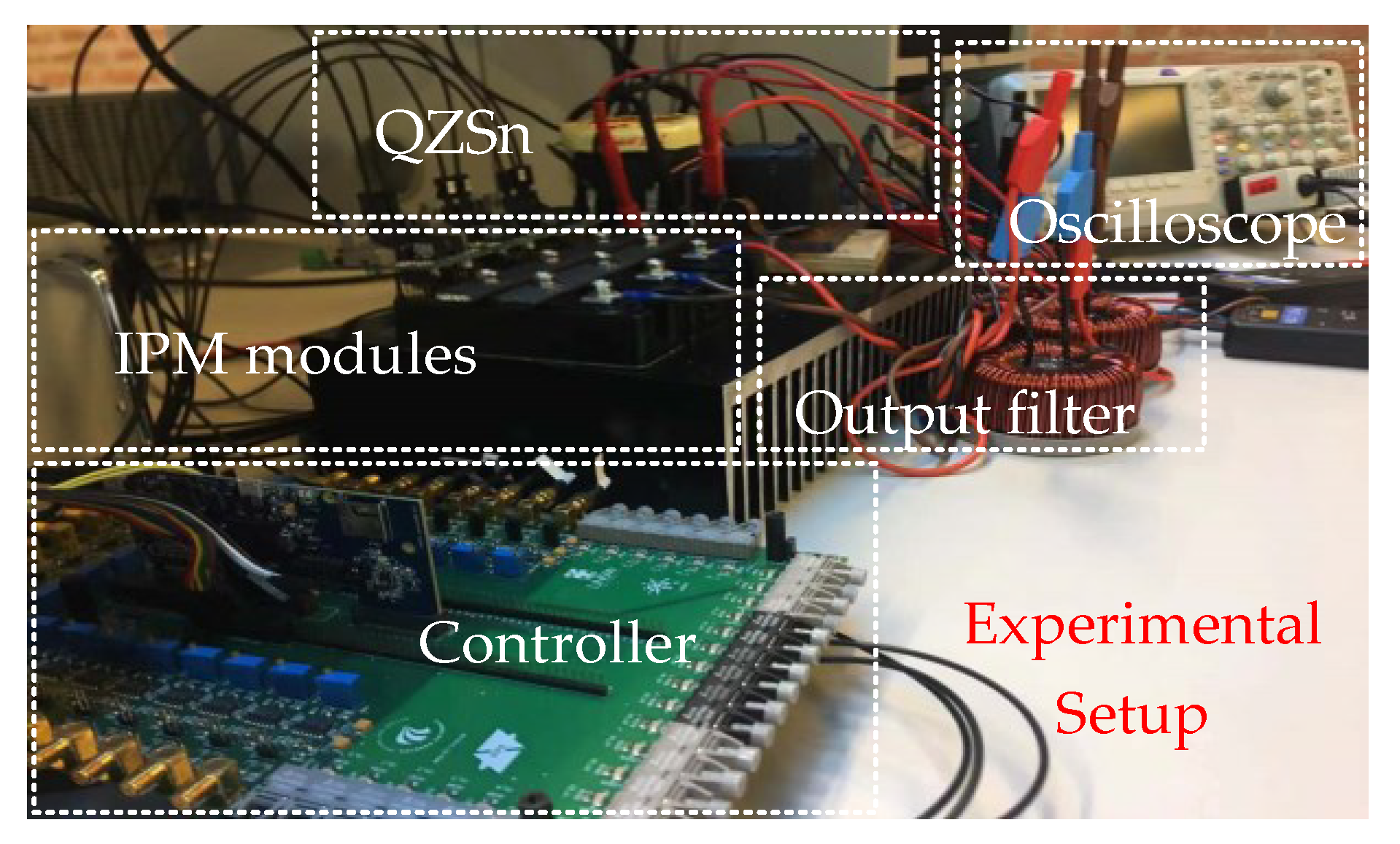
To verify the above analysis, simulations and experimental tests of the three-phase qZSI with the proposed CMV reduction strategies are presented. The system parameters of the qZSI are listed in Table 2. The simulations were implemented in MATLAB/Simulink. Meanwhile, the experimental tests were applied to the qZSI platform with a TMS320F28379 digital signal processor (DSP) controller, an Altera Cyclone field-programmable gate array (FPGA) and three Mitsubishi intelligent power modules (IPM), i.e., PM75DSA120.
The simulation results of the conventional qZSI system with the NSPWM and RSPWM strategies are presented in Figure 7a and Figure 8a. As shown in Figure 7a, the amplitude of the CMV with the NSPWM strategy varies from 0 to 133.3 V due to the adopted switching vectors, i.e., V 1 V 6 and V sh , referring to Table 1. The introduction of the ST state increases the CMV with more high-frequency components; see Figure 7a. The output current and voltage are also shown in Figure 7a, in which the peak-peak value of the load current is 10 A. Figure 8a shows the CMV value and the output of the conventional qZSI system. The amplitude of the CMV with the RSPWM strategy changes between 0 and 133.3 V when the chosen switching vectors are V 2 , V 4 , V 6 and V sh . The CMV of the conventional VSI with the RSPWM strategy is constant, but the CMV of the conventional qZSI with the RSPWM strategy contains high-frequency components, as shown in Figure 8a. The output current and voltage of the system present high total harmonic distortion (THD) (see Figure 8a), which results from the low DC-link utilization with only four switching vectors. This also occurs when the RSPWM strategy is used in the conventional VSI.
The simulation results of the modified qZSI system with RSPWM and NSPWM strategies are presented in Figure 7b and Figure 8b. The switching vectors for the two CMV reduction strategies are different, making the corresponding modified qZSI system not the same. According to (19), the relationship among L 11 , L 12 and L 1 is L 11 = L 12 = 1 2 L 1 when the proposed method is adopted in the qZSI system with the RSPWM strategy. The amplitude of the CMV with the NSPWM strategy on the modified qZSI system varies from 66.7 V to 123.3 V, as shown in Figure 7b, which is reduced dramatically when compared with that in Figure 7a. The output voltage and currents are exactly the same as that of the conventional qZSI system, which is not affected by the input split inductors. When the NSPWM strategy is used in the modified qZSI system, the relationship among L 11 , L 12 and L 1 is L 11 = 2 L 12 = 2 3 L 1 . As shown in Figure 8b, the CMV is constant at 120 V, and all the high-frequency components are removed, while the output characteristics are not affected. The modified qZSI system is related to the adopted switching vectors, which will not change the output of the system, but reduce CMV when using the conventional CMV reduction strategies.
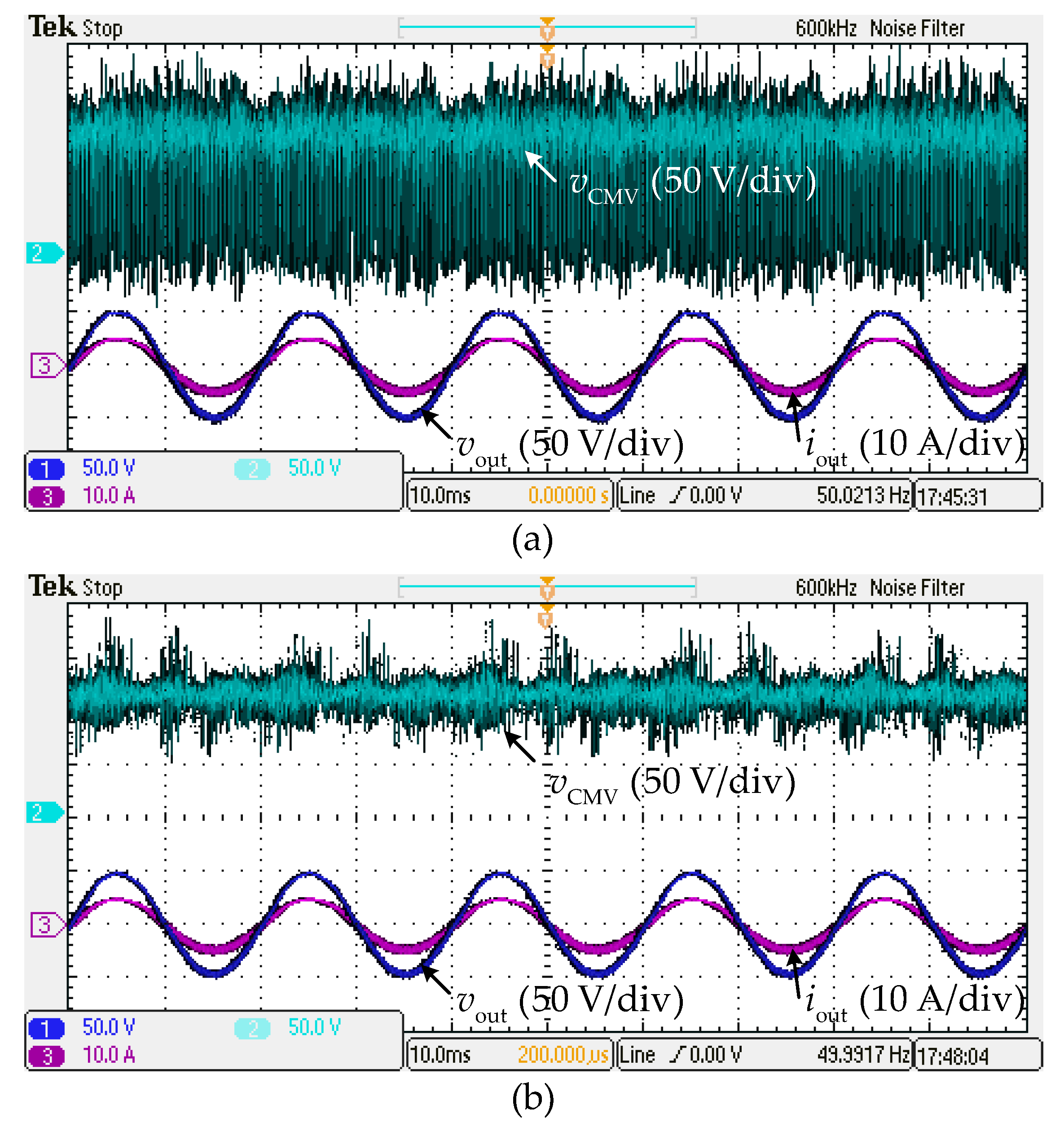
Figure 9 shows the experimental setup of the three-phase qZSI system. Figure 10 exemplifies the conventional qZSI system and the modified qZSI system when the RSPWM strategy is adopted. The experimental results agree well with the simulation results in Figure 8. The CMV of the conventional qZSI system contains high-frequency components when the ST state is used, which varies from 0 to 133.3 V, as shown in Figure 10a. With the split inductor of L 11 : L 12 = 2:1, the CMV is constant as 120 V using the RSPWM strategy in Figure 10b. The output characteristics of the conventional qZSI system and the modified qZSI system are the same, as shown in Figure 10, which verifies the effectiveness of the proposed CMV reduction strategy. The ST state is inserted in the zero states of the inverter, making the output of the inverter similar in the VSI, the qZSI and the modified qZSI when the same CMV reduction strategy is used. The total harmonic distortion (THD) of the output of the qZSI system is related to how many switching states exist in a switching cycle, which can be analysed exactly like the conventional VSI. When considering the output THD, CMV reduction strategies, e.g., the AZPWM and RSPWM strategies, can achieve a high-quality output compared to that with the NSPWM strategy in the VSI, the qZSI and the modified qZSI.

6. Conclusions

A CMV reduction strategy is proposed in this paper by splitting the input inductor to make the CMV reduction strategies for the conventional VSI available for the qZSI system. With the proposed strategy, the input inductor is divided into two parts at the positive and negative side of the input source with the same total inductance, keeping the continuous characteristics of the qZSI system. The ratio of the divided two-part inductance is related to the switching vectors that are chosen, which are generally used to reduce the CMV. The average CMV during the non-ST state is used to derive the proportional relationship between the divided inductance. With the proposed strategy, the output features are not affected, while the amplitude of the CMV is reduced. Simulations and experimental results are provided to verify the effectiveness of the proposed CMV reduction strategy. Moreover, the proposed CMV reduction strategy can also be used for other converters with a similar structure to reduce the CMV.

Author Contributions

Conceptualization, W.L., Y.Y. and T.K.; methodology, validation and formal analysis, W.L.; writing, review and editing, W.L., Y.Y., T.K., E.L., D.V. and F.B. All authors read and agreed to the published version of the manuscript.

Funding

This research received no external funding.

Acknowledgments

This research was supported in part by the Estonian Research Council (project PUT1443).

Conflicts of Interest

The authors declare no conflict of interest.

References

  1. Kerekes, T.; Koutroulis, E.; Sera, D.; Teodorescu, R.; Katsanevakis, M. An Optimization Method for Designing Large PV Plants. IEEE J. Photovolt. 2013, 3, 814–822. [Google Scholar] [CrossRef]
  2. Cacciato, M.; Consoli, A.; Scarcella, G.; Testa, A. Reduction of Common-Mode Currents in PWM Inverter Motor Drives. IEEE Trans. Ind. Appl. 1999, 35, 469–476. [Google Scholar] [CrossRef]
  3. Kerekes, T.; Teodorescu, R.; Liserre, M.; Klumpner, C.; Sumner, M. Evaluation of Three-Phase Transformerless Photovoltaic Inverter Topologies. IEEE Trans. Power Electron. 2009, 24, 2202–2211. [Google Scholar] [CrossRef]
  4. Bradaschia, F.; Cavalcanti, M.C.; Ferraz, P.E.P.; Azevedo, G.M.S.; Neves, F.A.S.; dos Santos, E.C. Stability Analysis of Reduced Leakage Current Modulation Techniques for Z-Source Inverters in Transformerless Photovoltaic Applications. In Proceedings of the ECCE, Delft, The Netherlands, 25–27 August 2011; pp. 2268–2275. [Google Scholar]
  5. Tang, Y.; Yao, W.; Loh, P.C.; Blaabjerg, F. Highly Reliable Transformerless Photovoltaic Inverters With Leakage Current and Pulsating Power Elimination. IEEE Trans. Ind. Electron. 2016, 63, 1016–1026. [Google Scholar] [CrossRef]
  6. Xiao, H.; Xie, S. Leakage Current Analytical Model and Application in Single-Phase Transformerless Photovoltaic Grid-Connected Inverter. IEEE Trans. Electromagn. Compat. 2010, 52, 902–913. [Google Scholar] [CrossRef]
  7. Yang, B.; Li, W.; Gu, Y.; Cui, W.; He, X. Improved Transformerless Inverter with Common-Mode Leakage Current Elimination for a Photovoltaic Grid-Connected Power System. IEEE Trans. Power Electron. 2012, 27, 752–762. [Google Scholar] [CrossRef]
  8. Kerekes, T.; Teodorescu, R.; Rodriguez, P.; Vazquez, G.; Aldabas, E. A New High-Efficiency Single-Phase Transformerless PV Inverter Topology. IEEE Trans. Ind. Electron. 2011, 58, 184–191. [Google Scholar] [CrossRef] [Green Version]
  9. Zhou, Y.; Huang, W.; Zhao, P.; Zhao, J. A Transformerless Grid-Connected Photovoltaic System Based on the Coupled Inductor Single-Stage Boost Three-Phase Inverter. IEEE Trans. Power Electron. 2014, 29, 1041–1046. [Google Scholar] [CrossRef]
  10. Liu, W.; Yang, Y.; Kerekes, T. Modified Quasi-Z-Source Inverter with Model Predictive Control for Constant Common-Mode Voltage. In Proceedings of the ICPE-ECCE Asia, Busan, Korea, 27–30 May 2019; pp. 1–6. [Google Scholar]
  11. Hava, A.M.; Ün, E. A High-Performance PWM Algorithm for Common-Mode Voltage Reduction in Three-Phase Voltage Source Inverters. IEEE Trans. Power Electron. 2011, 26, 1998–2008. [Google Scholar] [CrossRef]
  12. Hou, C.C.; Shih, C.C.; Cheng, P.T.; Hava, A.M. Common-Mode Voltage Reduction Pulsewidth Modulation Techniques for Three-Phase Grid-Connected Converters. IEEE Trans. Power Electron. 2013, 28, 1971–1979. [Google Scholar] [CrossRef]
  13. Kerekes, T.; Teodorescu, R.; Liserre, M. Common Mode Voltage in Case of Transformerless PV Inverters Connected to the Grid. In Proceedings of the ISIE, Cambridge, UK, 30 June–2 July 2008; IEEE: Cambridge, UK, 2008; pp. 2390–2395. [Google Scholar]
  14. Buticchi, G.; Barater, D.; Lorenzani, E.; Franceschini, G. Digital Control of Actual Grid-Connected Converters for Ground Leakage Current Reduction in PV Transformerless Systems. IEEE Trans. Ind. Inform. 2012, 8, 563–572. [Google Scholar] [CrossRef]
  15. Hoseini, S.K.; Sheikholeslami, A.; Adabi, J. Predictive Modulation Schemes to Reduce Common-Mode Voltage in Three-Phase Inverters-Fed AC Drive Systems. IET Power Electron. 2014, 7, 840–849. [Google Scholar] [CrossRef]
  16. Rojas, C.A.; Aguirre, M.; Kouro, S.; Geyer, T.; Gutierrez, E. Leakage Current Mitigation in Photovoltaic String Inverter Using Predictive Control With Fixed Average Switching Frequency. IEEE Trans. Ind. Electron. 2017, 64, 9344–9354. [Google Scholar] [CrossRef]
  17. Kakosimos, P.; Abu-Rub, H. Predictive Control of a Grid-Tied Cascaded Full-Bridge NPC Inverter for Reducing High-Frequency Common-Mode Voltage Components. IEEE Trans. Ind. Inform. 2018, 14, 2385–2394. [Google Scholar] [CrossRef]
  18. Wang, X.; Zou, J.; Ma, L.; Zhao, J.; Xie, C.; Li, K.; Meng, L.; Guerrero, J.M. Model Predictive Control Methods of Leakage Current Elimination for a Three-Level T-Type Transformerless PV Inverter. IET Power Electron. 2018, 11, 1492–1498. [Google Scholar] [CrossRef]
  19. Mun, S.k.; Kwak, S. Reducing Common-Mode Voltage of Three-Phase VSIs Using the Predictive Current Control Method Based on Reference Voltage. J. Power Electron. 2015, 15, 712–720. [Google Scholar] [CrossRef]
  20. Anderson, J.; Peng, F.Z. Four Quasi-Z-Source Inverters. In Proceedings of the PESC, Rhodes, Greece, 15–19 June 2008; pp. 2743–2749. [Google Scholar]
  21. Siwakoti, Y.P.; Peng, F.Z.; Blaabjerg, F.; Loh, P.C.; Town, G.E. Impedance-Source Networks for Electric Power Conversion Part I: A Topological Review. IEEE Trans. Power Electron. 2015, 30, 699–716. [Google Scholar] [CrossRef]
  22. Siwakoti, Y.P.; Peng, F.Z.; Blaabjerg, F.; Loh, P.C.; Town, G.E.; Yang, S. Impedance-Source Networks for Electric Power Conversion Part II: Review of Control and Modulation Techniques. IEEE Trans. Power Electron. 2015, 30, 1887–1906. [Google Scholar] [CrossRef]
  23. Liu, W.; Yuan, J.; Yang, Y.; Kerekes, T. Modeling and Control of Single-Phase Quasi-Z-Source Inverters. In Proceedings of the IECON, Washington, DC, USA, 21–23 October 2018; pp. 3737–3742. [Google Scholar]
  24. Liu, W.; Yang, Y.; Kerekes, T. Characteristic Analysis of the Grid-Connected Impedance-Source Inverter for PV Applications. In Proceedings of the PEDG, Xi’an, China, 3–6 June 2019; pp. 874–880. [Google Scholar]
  25. Guo, X.; Zhou, J.; He, R.; Jia, X.; Rojas, C.A. Leakage Current Attenuation of a Three-Phase Cascaded Inverter for Transformerless Grid-Connected PV Systems. IEEE Trans. Ind. Electron. 2018, 65, 676–686. [Google Scholar] [CrossRef]
  26. Noroozi, N.; Zolghadri, M.R.; Yaghoubi, M. Comparison of Common-Mode Voltage in Three-Phase Quasi-Z-Source Inverters Using Different Shoot-through Implementation Methods. In Proceedings of the CPE-POWERENG, Doha, Qatar, 10–12 April 2018; IEEE: Piscataway, NJ, USA, 2018; pp. 1–6. [Google Scholar]
  27. Noroozi, N.; Zolghadri, M.R. Three-Phase Quasi-Z-Source Inverter with Constant Common-Mode Voltage for Photovoltaic Application. IEEE Trans. Ind. Electron. 2018, 65, 4790–4798. [Google Scholar] [CrossRef]
  28. Guo, X.; Yang, Y.; Wang, B.; Blaabjerg, F. Leakage Current Reduction of Three-Phase Z-Source Three-Level Four-Leg Inverter for Transformerless PV System. IEEE Trans. Power Electron. 2019, 34, 6299–6308. [Google Scholar] [CrossRef]
  29. Guo, X.; Yang, Y.; He, R.; Wang, B.; Blaabjerg, F. Transformerless Z-Source Four-Leg PV Inverter With Leakage Current Reduction. IEEE Trans. Power Electron. 2019, 34, 4343–4352. [Google Scholar] [CrossRef]
  30. Meraj, M.; Rahman, S.; Iqbal, A.; Ben–Brahim, L. Common Mode Voltage Reduction in A Singlephase Quasi Z-Source Inverter for Transformerless Grid-Connected Solar PV Applications. IEEE J. Emerg. Sel. Top. Power Electron. 2018, 7, 1352–1363. [Google Scholar] [CrossRef]
  31. Liu, W.; Yang, Y.; Kerekes, T.; Blaabjerg, F. Generalized Space Vector Modulation for Ripple Current Reduction in Quasi-Z-Source Inverters. IEEE Trans. Power Electron. 2021, 36, 1730–1741. [Google Scholar] [CrossRef]
  32. Kayiranga, T.; Li, H.; Lin, X.; Shi, Y.; Li, H. Abnormal Operation State Analysis and Control of Asymmetric Impedance Network-Based Quasi-Z-Source PV Inverter (AIN-qZSI). IEEE Trans. Power Electron. 2016, 31, 7642–7650. [Google Scholar] [CrossRef]
  33. Bradaschia, F.; Cavalcanti, M.C.; Ferraz, P.E.P.; Neves, F.A.S.; dos Santos, E.C.; da Silva, J.H.G.M. Modulation for Three-Phase Transformerless Z-Source Inverter to Reduce Leakage Currents in Photovoltaic Systems. IEEE Trans. Ind. Electron. 2011, 58, 5385–5395. [Google Scholar] [CrossRef]
Figure 1. Schematic of a three-phase grid-connected quasi-Z-source inverter system, where the quasi-Z-source network (qZSn) consists of two inductors L 1 , L 2 , two capacitors C 1 , C 2 and a diode D, L f is the output filter, v g is the grid voltage, C pv is the parasitic capacitance between the PV array and the ground and i leak is the leakage current.
Applsci 10 08713 g001
Figure 2. Equivalent circuits of the quasi-Z-source inverter during the (a) active state, (b) null state and (c) shoot-through state.
Applsci 10 08713 g002
Figure 3. Switching vectors generated by the qZSI in the vector space.
Applsci 10 08713 g003
Figure 4. Typical CMV reduction strategies with switching patterns and CMV when using: (a) discontinuous pulse width modulation (DPWM), (b) active zero state pulse width modulation (AZSPWM), (c) remote state pulse width modulation (RSPWM) and (d) near state pulse width modulation (NSPWM) strategies.
Applsci 10 08713 g004
Figure 5. Proposed CMV reduction strategies with switching patterns and CMV when using DPWM, AZPWM, RSPWM and NSPWM strategies.
Applsci 10 08713 g005
Figure 6. Modified quasi-Z source inverter system with a split inductor.
Applsci 10 08713 g006
Figure 7. Simulation results of the CMV v cmv , output voltage v out and output voltage i out when the NSPWM strategy is used in (a) the conventional three-phase qZSI system and (b) the modified three-phase qZSI system [Time (5 ms/div)].
Applsci 10 08713 g007
Figure 8. Simulation results of the CMV v cmv , output voltage v out and output voltage i out when the RSPWM strategy is used in (a) the conventional three-phase qZSI system and (b) the modified three-phase qZSI system [Time (5 ms/div)].
Applsci 10 08713 g008
Figure 9. Photograph of the experimental setup of the three-phase qZSI system.
Applsci 10 08713 g009
Figure 10. Experimental results of the CMV v cmv , output voltage v out and output voltage i out when the RSPWM strategy, i.e., all even vectors in this paper, is used in (a) the conventional three-phase qZSI system and (b) the modified three-phase qZSI system [Time (10 ms/div)].
Applsci 10 08713 g010
Table 1. CMVs with relevant vectors in the qZSI.
VectorsCMV Values
V 1 , V 3 , V 5 (odd vectors) 1 3 V DC
V 2 , V 4 , V 6 (even vectors) 2 3 V DC
V 7 (zero vector) V DC
V 0 (zero vector)0
V st (shoot-through vectors)0
Table 2. Parameters of the three-phase qZSI system.
ParametersSymbolValues
Input voltage V in 160 V
qZSI inductors L 1 , L 2 700 μ H
qZSI inductor resistance R L 1 0.05 Ω
qZSI capacitors C 1 , C 2 200 μ F
qZSI capacitor resistance R C 1 0.05 Ω
Output filter L f 1.8 mH
Switching frequency f s 10 kHz
Shoot-through duty ratio D sh 0.1
Publisher’s Note: MDPI stays neutral with regard to jurisdictional claims in published maps and institutional affiliations.