Article

A Novel Top-Down Fabrication Process for Vertically-Stacked Silicon-Nanowire Array
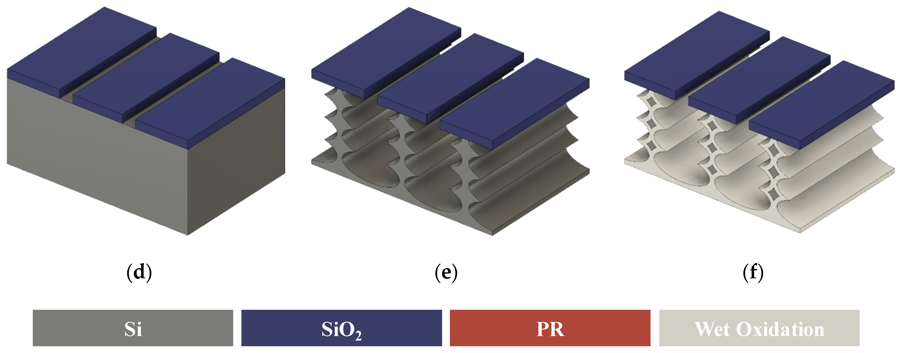
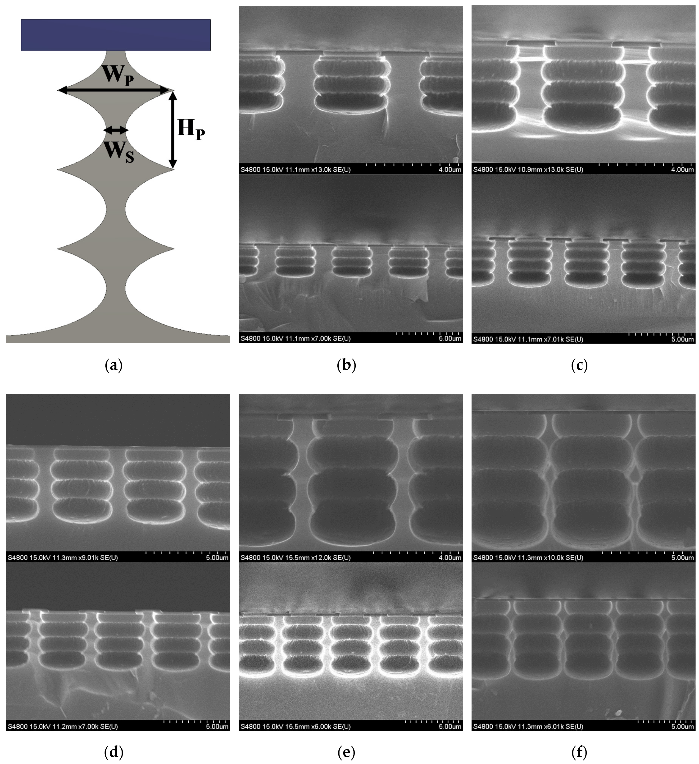
Department of Biomedical Engineering, Kyung Hee University, Yongin 17104, Korea
*
Author to whom correspondence should be addressed.
Appl. Sci. 2020, 10(3), 1146; https://doi.org/10.3390/app10031146
Submission received: 19 December 2019 / Revised: 29 January 2020 / Accepted: 4 February 2020 / Published: 8 February 2020
(This article belongs to the Special Issue Selected Papers from IMETI 2018)

Abstract

Silicon nanowires are widely used for sensing applications due to their outstanding mechanical, electrical, and optical properties. However, one of the major challenges involves introducing silicon-nanowire arrays to a specific layout location with reproducible and controllable dimensions. Indeed, for integration with microscale structures and circuits, a monolithic wafer-level process based on a top-down silicon-nanowire array fabrication method is essential. For sensors in various electromechanical and photoelectric applications, the need for silicon nanowires (as a functional building block) is increasing, and thus monolithic integration is highly required. In this paper, a novel top-down method for fabricating vertically-stacked silicon-nanowire arrays is presented. This method enables the fabrication of lateral silicon-nanowire arrays in a vertical direction, as well as the fabrication of an increased number of silicon nanowires on a finite dimension. The proposed fabrication method uses a number of processes: photolithography, deep reactive-ion etching, and wet oxidation. In applying the proposed method, a vertically-aligned silicon-nanowire array, in which a single layer consists of three vertical layers with 20 silicon nanowires, is fabricated and analyzed. The diamond-shaped cross-sectional dimension of a single silicon nanowire is approximately 300 nm in width and 20 μm in length. The developed method is expected to result in highly-sensitive, reproducible, and low-cost silicon-nanowire sensors for various biomedical applications.
Keywords: silicon nanowire; top-down fabrication; monolithic process; vertically-stacked array silicon nanowire; top-down fabrication; monolithic process; vertically-stacked array

