Article

Electrical Coupling of Monolithic 3D Inverters (M3INVs): MOSFET and Junctionless FET

1
Department of Electrical, Electronic and Control Engineering and IITC, Hankyong National University, Anseong 17579, Korea
2
Group for Smart Energy Nano Convergence, Korea Institute of Industrial Technology, Gwangju 61012, Korea
*
Author to whom correspondence should be addressed.
Appl. Sci. 2021, 11(1), 277; https://doi.org/10.3390/app11010277
Submission received: 5 December 2020 / Revised: 23 December 2020 / Accepted: 28 December 2020 / Published: 30 December 2020
(This article belongs to the Special Issue Device Modeling for TCAD and Circuit Simulation)

Abstract

:
In this paper, we investigated the electrical coupling between the top and bottom transistors in a monolithic 3-dimensional (3D) inverter (M3INV) stacked vertically with junctionless field-effect transistor (JLFET), which is one of candidates to replace metal-oxide-semiconductor field-effect transistors (MOSFET). Currents, transconductances, and gate capacitances of the top N-type transistor at the different gate voltages of the bottom P-type transistor as a function of thickness of inter-layer dielectric (TILD) and gate channel length (Lg) are simulated using technology computer-aided-design (TCAD). In M3INV stacked vertically with MOSFET (M3INV-MOS) and JLFET (M3INV-JL), the variations of threshold voltage, transconductance, and capacitance increase as TILD decreases and they increase as Lg increases, and thus there is a strong coupling in M3INV at the range of TILD ≤ 30 nm. In M3INV, the coupling between stacked JLFETs in M3INV-JL is larger than that between MOSFETs in M3INV-MOS at the same TILD and Lg. The switching threshold voltage (Vm) and noise margins (NMs) of M3INV are calculated from the voltage transfer characteristics (VTC) simulated with TCAD mixed-mode. As the gate lengths of M3INV-MOS and M3INV-JL increase, the Vm variations increase and decrease, respectively. The smaller the gate lengths of M3INV-NOS and M3INV-JL, the larger and smaller the variation of Vm, respectively. The noise margin of M3INV-MOS is larger and better for inverter characteristics than one of M3INV-JL. M3INV-MOS has less electrical coupling than M3INV-JL.

1. Introduction

Since metal-oxide-semiconductor field-effect transistors (MOSFETs) were developed, the performance of semiconductor integrated circuits has been steadily developed in accordance with Moore’s Law [1]. Semiconductor devices with the gate length of less than 10 nm, which are core technologies required for the 4th industrial revolution such as artificial intelligence (AI), internet of thing (IOT), cloud computing, big data, and virtual reality [2], have been developing. As the process technology advances by scaling-down, the physical limitations of silicon-based semiconductor processes and the increased integration have led to the problems in thermal budget, delay, and power consumption [3]. In order to solve such problems, various types of researches related on developments of semiconductor materials, process technology, and devices have been actively carried out [4]. The monolithic 3-dimensional (3D) integrated-circuit (M3IC), which vertically stacks each tier on a previously fabricated tier, is one of the promising techniques to break the physical limits [5,6]. This technology is more advantageous in density, delay, and cost because of the smaller length of the Via than the existing parallel integration which makes devices on each wafer and connects them with through-silicon via (TSV) between wafers [7]. This is one of the main problems with M3IC which has the reduction the thermal budget of the MOSFETs in the 2nd and subsequent tiers on the M3DIC [8,9]. MOSFET and junctionless field-effect transistor (JLFET) have opposite operating principles. The MOSFET controls the current through depletion and inversion, and the JLFET controls the current with or without depletion. MOSFET has different source/drain and channel doping types (n/p), whereas JLFET use one doping type for source/drain and channel. Therefore, JLFET is advantageous in terms of thermal budget because the dopant activation process of the MOSFET is unnecessary. The thermal budget of upper tier is constrained by maximum thermal budget of the lower tier or tiers. JLFET has little effect of short channel effect, which is a major problem in MOSFET, and shows good performance in terms of carrier mobility. In order to solve the thermal budget problem, enhance the immunity of mobility degradation, and possess the simplicity of fabrication, JLFET [10,11] on M3IC has been proposed as the replacement of MOSFET [12].
M3IC technology stacking field-programmable gate-array (FPGA) logics and sensor devices have been reported, but the M3IC consisted of stacked MOSFETs and its thickness of interlayer dielectric (ILD), TILD, between vertically stacked devices was over 100 nm so that there are no electrical coupling between stacking devices [9]. Recently, a study considering the electrical coupling between stacked devices has been performed when the ILD in monolithic 3D inverter (M3INV) consisting of MOSFETs is very thin (i.e., TILD < 50 nm) [13,14]. Interlayer coupling in monolithic 3D static random access memory (M3SRAM) stacked vertically with tunnel field-effect transistor (TFET) and MOSFET has been investigated in terms of stability and performance [15]. However, no research has been reported on the electrical coupling between the upper and lower devices of the M3IC consisting of JLFET [16] which can replace the MOSFETs.
Therefore, it is necessary to investigate the electrical interaction between devices in M3IC stacked with the next generation devices. In this paper, we will introduce the electrical coupling in terms of thickness variation of ILD in M3INV stacked vertically with JLFETs, compared with one with MOSFETs. The structures and simulation method of the M3INV with MOSFETs or JLFETs will be introduced (Section 2), and the electrical coupling of upper device at different gate voltage of lower devices, simulated with the DC/AC device parameter, will be investigated (Section 3). In Section 4, electrical characteristics of two types of M3INV (MOSFETs and JLFETs) will be explained. Finally, Section 5 concludes.

2. Structure and Simulation Method

Figure 1 shows two types of M3INV structures used in the simulation. The M3INV consists of N-type and P-type transistors in the upper and lower tiers, respectively. Figure 1a,b are schematics of M3INV consisting of MOSFET (M3INV-MOS) [5] and JLFET (M3INV-JL) [12], respectively. The doping concentrations of source/drain, LDD, and channel in MOSINV-MOS are 1021, 1018, and 1015 cm−3, respectively [13,14]. The doping concentrations of source/drain and channel of M3INV-JL is 1020 and 1019 cm−3, respectively [12]. The detailed parameters in both M3INV-MOS and M3INV-JL are shown in Table 1. Three types of structures for both M3INV-MOS and M3INV-JL are simulated: gate lengths/gate oxide thicknesses are 20/0.9 nm, 30/1 nm, and 50/1.1 nm, respectively [14]. SiO2 was used for the regions in gate oxide, ILD, and bulk oxide (Box). Figure 1c shows the equivalent circuit of M3INV-MOS and M3DINV-JL. Silvaco’s technology computer-aided-design (TCAD) simulator ATLAS [17] was used in this simulation. The models used in the simulation are CVT, SRH, AUGER, and FERMI. The leakage currents of both MOSFET and JLFET in each M3INV were set equal to 10−8 A, in order to simulate the inverter characteristics with same leakage current condition. The Vth variation, gm variation, Cngng variation, Vm, and noise margin of both M3INV-MOS and M3INV-JL were compared through TCAD simulation.

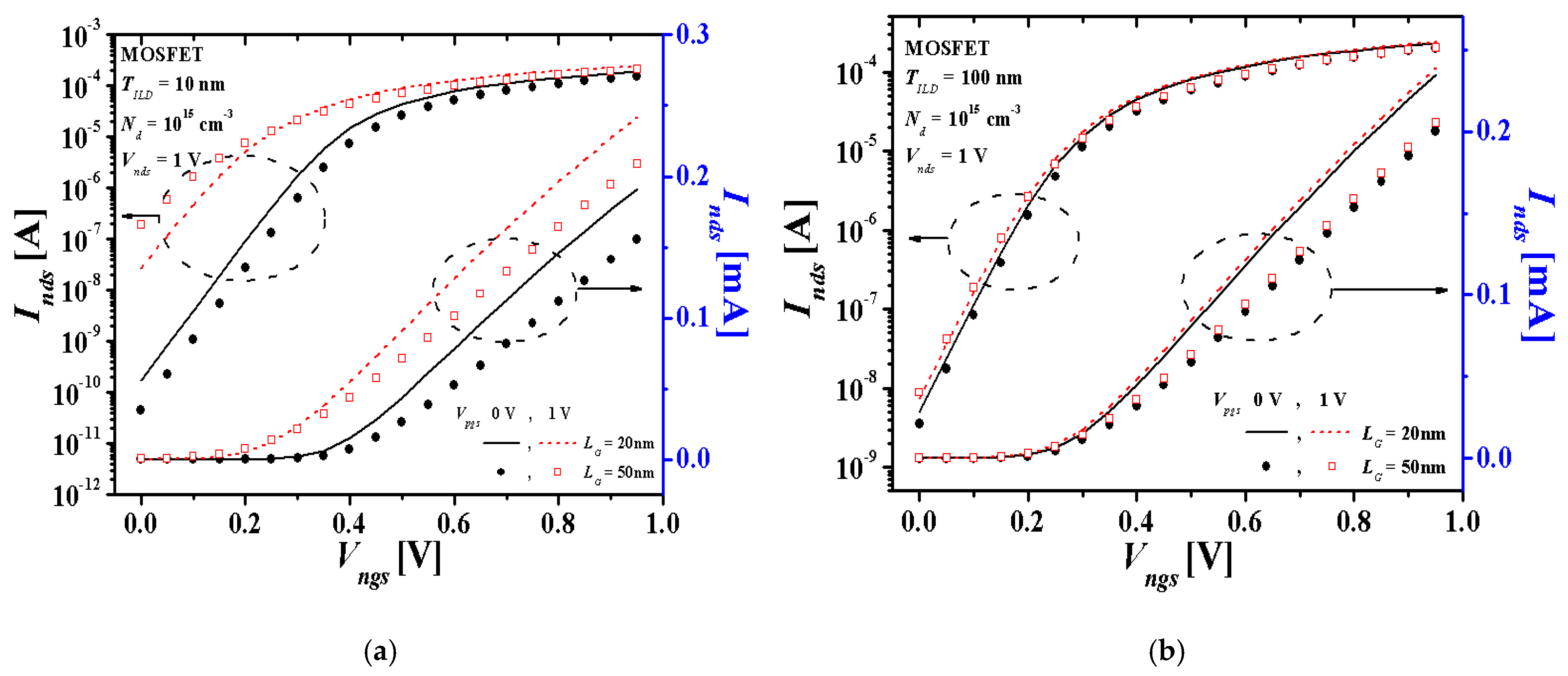
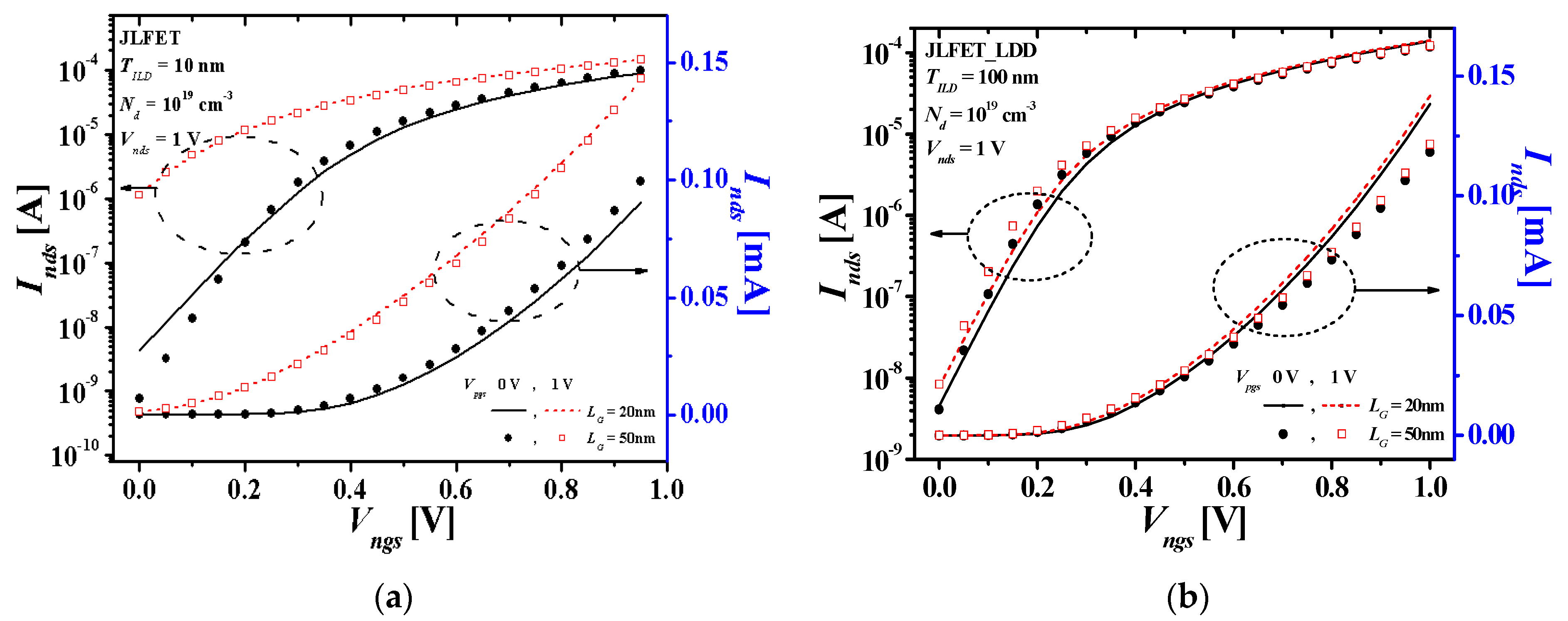
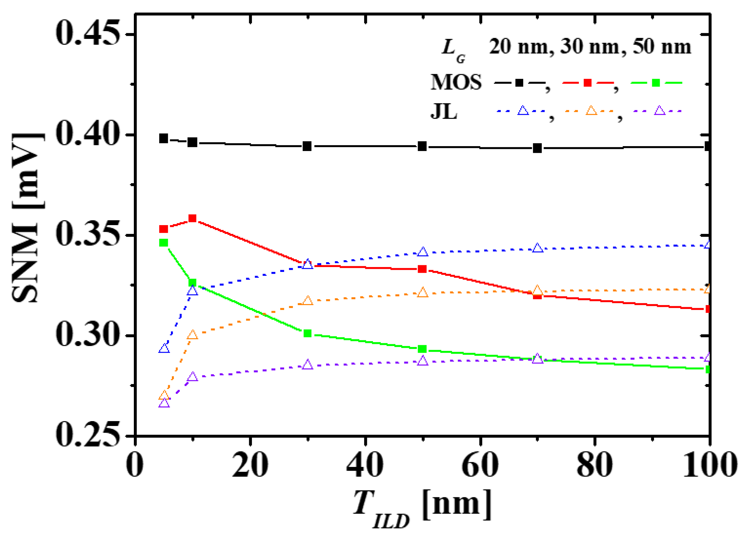
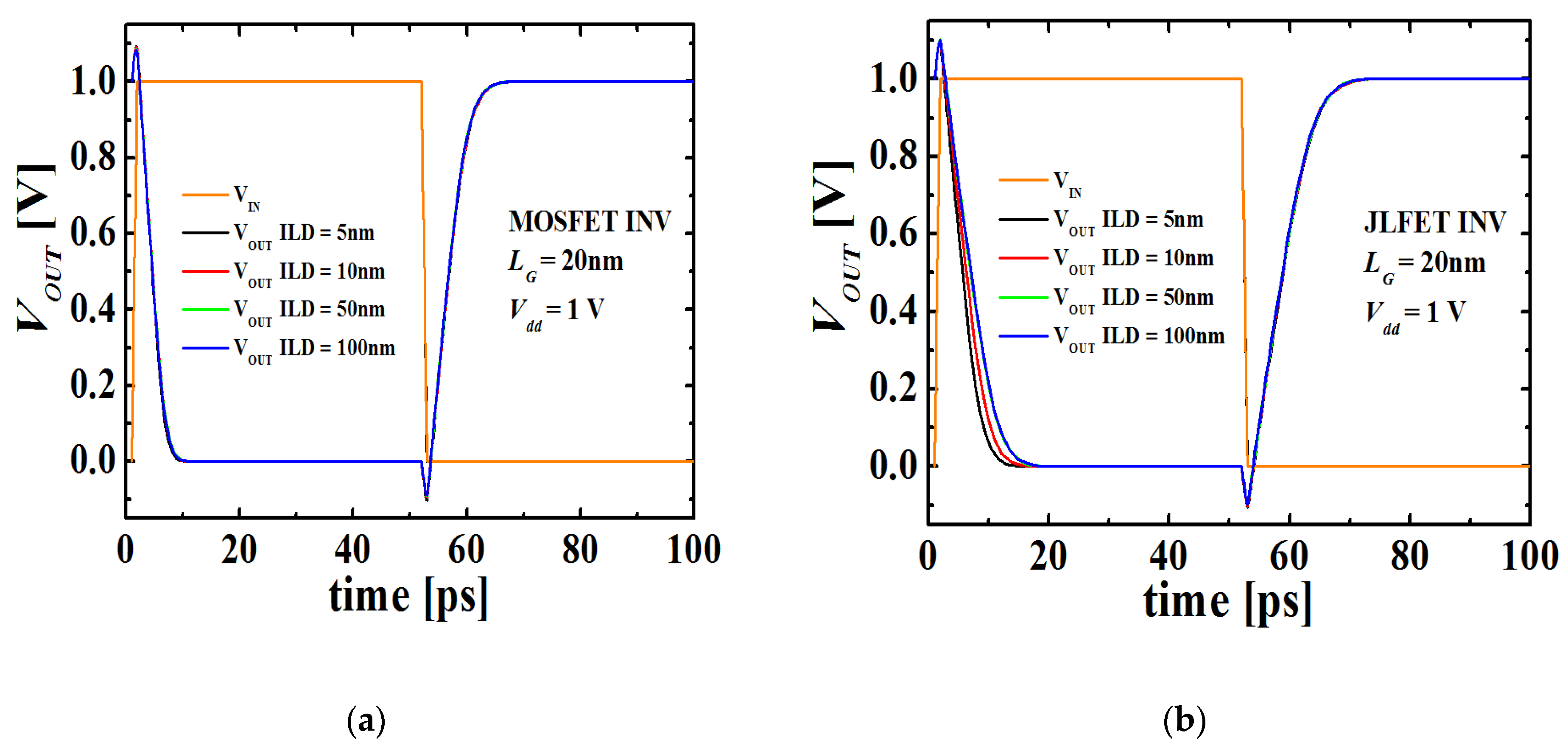
3. DC/AC Characteristics

Figure 2 and Figure 3 show the drain current-gate voltage (Inds-Vngs) characteristics of two types of top N-type transistors (LG = 20 and 50 nm) in M3INV-MOS and M3INV-JL at the different gate voltages (=0 and 1 V) of bottom P-type transistor, respectively. The solid lines and dotted lines indicate Inds-Vngs characteristics of top N-type transistors with LG = 20 nm at two different gate voltages (=0 V and 1 V) of the bottom P-type transistors, respectively, and the squares and the circles Inds-Vngs characteristics of top N-type transistors with LG = 50 nm at two different gate voltages (=0 V and 1 V) of the bottom P-type transistors, respectively. Figure 2 show Inds-Vngs characteristics of top N-type MOSFET in M3INV-MOS in the case of TILD = 10 nm and 100 nm, respectively. Figure 3 show Inds-Vngs characteristics of top N-type JLFET in M3INV-JL in the case of TILD = 10 nm and 100 nm, respectively. When TILD = 10 nm, it can be observed that the threshold voltage of top N-type transistors was clearly shifted due to the gate voltage of bottom P-type transistor. On the other hand, in the case of TILD = 100 nm, no threshold voltage shift of top N-type transistors occurs when the gate voltage of bottom P-type transistors changes.
Figure 4 show ΔVth, ΔVgm, and ΔVCngng versus TILD at different gate lengths (LG = 20, 30, and 50 nm) of the top N-type transistors in both M3INV-MOS and MOSINV-JL, respectively. The filled and empty symbols denote simulation results of the top N-type transistors in both M3INV-MOS and M3INV-JL, respectively, and the squares, circles, and triangles denote those at LG = 20, 30, and 50 nm, respectively. As TILD decreases, ΔVth, ΔVgm, and ΔVCngng increases at both M3INV-MOS and M3INV-JL. When TILD is over 30 nm, ΔVth, ΔVgm, and ΔVCngng are below 50 mV, the coupling between stacked transistors in both M3INV-MOS [14] and M3INV-JL can be ignored. As LG increases in both M3INV-MOS and M3INV-JL, ΔVth, ΔVgm, and ΔVCngng increase. ΔVth, ΔVgm, and ΔVCngn of M3INV-JL has larger than those of M3INV-MOS as TILD decreases, and the average variations of ΔVth and ΔVgm in M3INV-JL are smaller than those in M3INV-MOS as LG increases, but the variation of ΔVCngng does not depend on LG at both M3INV-MOS and M3INV-JL. As the channel length decreases, PN+ junction in M3DINV-MOS makes the effective channel length decrease, resulting in short-channel effects (SCEs), but the junctionless in M3DINV-JL can make the SCEs decrease [18,19,20]. Because JLFET is more immune than MOSFET with PN junction in terms of SCE, the average variations of ΔVth and ΔVgm in M3INV-JL are smaller than those in M3INV-MOS as LG decreases. In the case of both M3INV-MOS and M3INV-JL, these results are dependent on the bottom-gate voltage variation (ΔVpgs) are similar to the classical capacitive coupling ratio γ (=ΔVthVpgs) of asymmetric double-gate (DG) ultra-thin body silicon on insulator (UTB-SOI) MOSFET [21] because both structures of the top N-type transistors in M3INV-MOS and M3INV-JL are similar to one of asymmetric DG UTB-SOI MOSFET. As TILD decreases, γ increases [14,21], as follows.
γ = T o x + ε o x ε S i X b a r T I L D + ε o x ε S i ( T S i X b a r ) ,
where Xbar means the distance between the front SiO2/Si interface and barycenter location of charge in the silicon channel [22] of the top N-type transistors in both M3INV-MOS and M3INV-JL. Because the barycenter of the top N-type transistors in M3INV-MOS and M3INV-JL are located close to the front SiO2/Si interface and the center in silicon-channel, respectively, γ of the top N-type transistors in M3INV-JL is higher than one of M3INV-MOS, as shown in Figure 4. The threshold conditions of M3INV-MOS and M3INV-JL define strongly-inverted and fully-depleted in all the channel, respectively. In the threshold regime of M3INV-MOS and M3INV-JL, the back SiO2/Si interfaces on both top N-type transistors are depleted without any accumulation [21] and inversion [20], respectively. It is noted that dependence of back-gate voltage for full-depletion in all the channel of M3INV-JL is larger than one for strong inversion of M3INV-MOS.

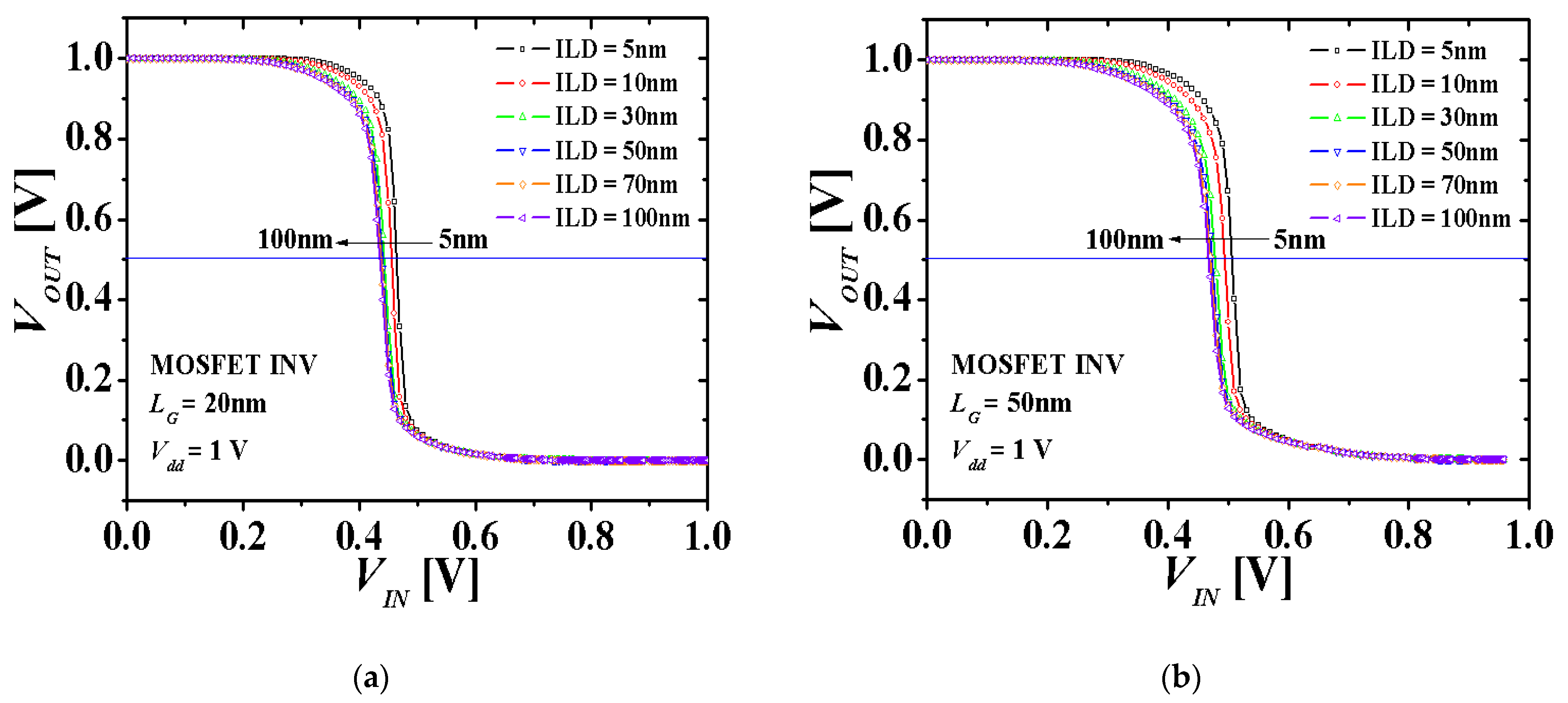
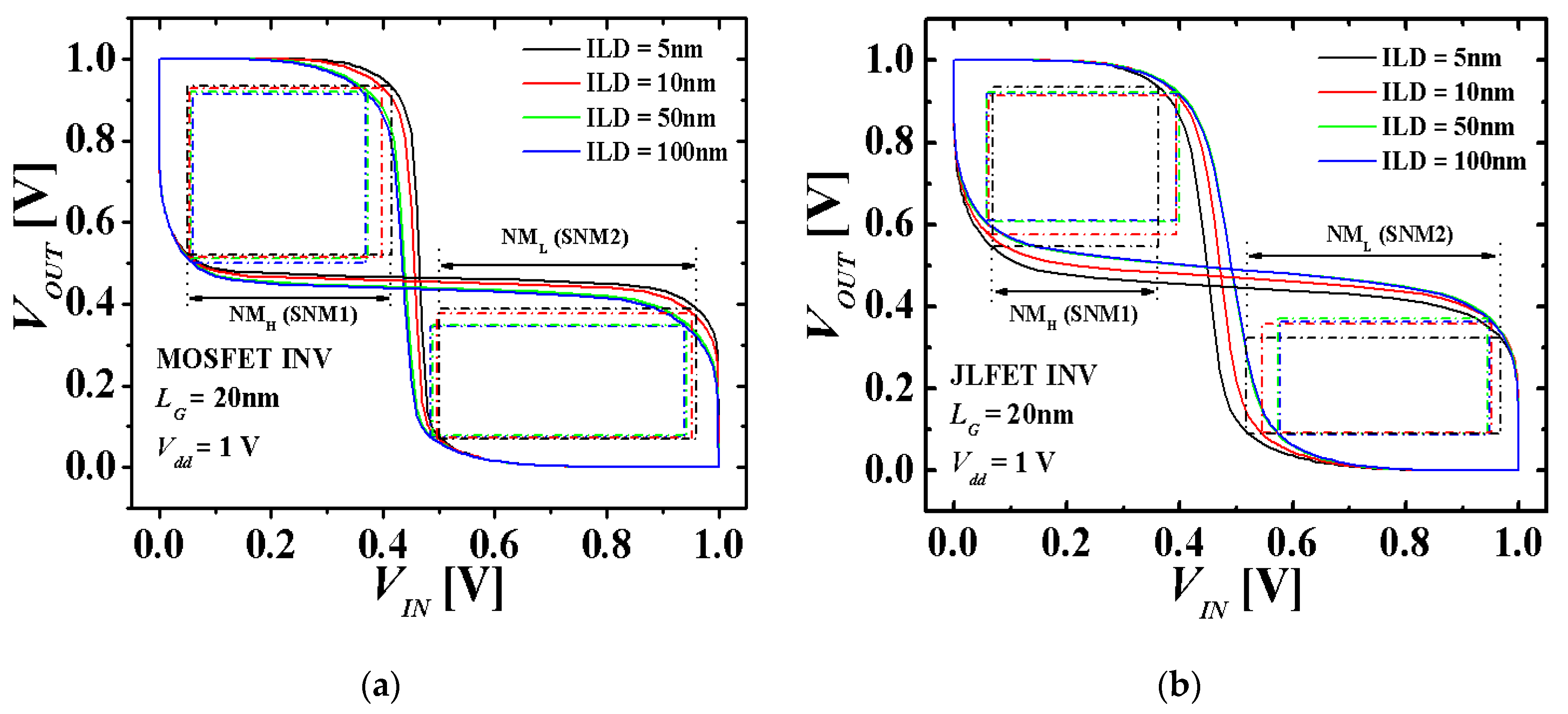
4. Inverter Characteristics

Mixed-mode circuit simulation of ATLAS was used to verify the inverter characteristics by both M3INV-MOS and M3INV-JL including the electrical coupling.
Figure 5 and Figure 6 show the voltage transfer characteristics (VTC) of M3INV-MOS and M3INV-JL, respectively. Figure 5a and Figure 6a show the simulation results of LG = 20 nm and Figure 5b and Figure 6b show those of LG = 50 nm. M3INV-MOS shifts VTC from right to left as TILD increases, but M3INV-JL shifts VTC from left to right as TILD increases.
Figure 7 shows ΔVm versus TILD of both M3INV-MOS and M3INV-JL. As TILD decreases, ΔVm increases. When TILD is over 30 nm, ΔVm are below 10 mV, and thus the coupling in the structures can be ignored. In the case of M3INV-MOS, the larger LG, the larger ΔVm, but in the case of M3INV-JL, the smaller LG, the larger ΔVm.
Figure 8 show the static noise margin (SNM) windows of M3INV-MOS and M3INV-JL with LG = 20 nm, respectively. The SNMs were measured as noise margin high (NMH) and noise margin low (NML) extracted from VTCs of M3INV-MOS and M3INV-JL. Figure 9 shows the noise margins of M3INV-MOS and M3INV-JL at different LGs and TILDs. In the case of M3INV-MOS, SNM increases as TILD decreases. On the other hand, in the case of M3INV-JL, SNM decreases when TILD decreases. When TILD is over 30 nm, the maximum variations of SNM of both M3INV-MOS and M3INV-JL are below 20 mV, and thus the coupling in both structures can be also ignored.
Figure 10 show the transient responses of M3INV-MOS and M3INV-JL with LG = 20 nm at different TILDs, respectively. Table 2 shows the propagation delays extracted from the transient response in Figure 10. As TILD decreases, propagation delays of M3INV-MOS and M3INV-JL increase and decrease, respectively. As LG increases, propagation delays of both M3INV-MOS and M3INV-JL increase. When TILD is over 30 nm, the maximum variations of propagation delay of both M3INV-MOS and M3INV-JL are below 0.2 ps, and thus the coupling in the structures can be also ignored.

5. Conclusions

In this paper, we investigated the electrical coupling through the threshold voltage, transconductance, and gate capacitance variation according to TILD of M3INV-MOS and M3INV-JL through TCAD simulation and compared the VTC and Vm and SNM characteristics in M3INV-MOS and M3INV-JL. In both M3INV-MOS and M3INV-JL, ΔVth, ΔVgm, and ΔVCngng increase as TILD decreases. The smaller LG, the larger ΔVth and ΔVgm, but ΔVCngng is not significant. In addition, as TILD increased, M3INV-MOS and M3INV-JL shifted VTCs from right to left and from left to right, respectively. The larger LG, the larger and smaller ΔVm of M3INV-MOS and M3INV-JL, respectively. The noise margin and inverter characteristics of M3INV-MOS is larger and better than those of M3INV-JL. M3INV-MOS has less electrical coupling in terms of ΔVth, ΔVgm, ΔVCngng, ΔVm, NMH, NML, and propagation delay than M3INV-JL. When TILD is over 30 nm, ΔVth, ΔVgm, and ΔVCngng are below 50 mV, ΔVm are below 10 mV, the maximum variations of SNM of both M3INV-MOS and M3INV-JL are below 20 mV, and the maximum variations of propagation delay of both M3INV-MOS and M3INV-JL are below 0.2 ps, and thus the coupling in the structures can be ignored.

Author Contributions

Conceptualization, T.J.A. and Y.S.Y.; methodology, T.J.A. and Y.S.Y.; investigation, T.J.A. and Y.S.Y.; data curation, T.J.A.; writing—original draft preparation, T.J.A.; writing—review and editing, T.J.A. and Y.S.Y.; supervision, Y.S.Y.; project administration, Y.S.Y.; funding acquisition, Y.S.Y. All authors have read and agreed to the published version of the manuscript.

Funding

This research was supported by the Basic Science Research Program through the National Research Foundation of Korea (NRF) funded by the Ministry of Education (NRF-2019R1A2C1085295).

Institutional Review Board Statement

Not applicable.

Informed Consent Statement

Not applicable.

Data Availability Statement

The raw/processed data required to reproduce these findings will be shared upon request from the corresponding author.

Acknowledgments

This work was supported by IDEC (EDA tool).

Conflicts of Interest

The authors declare no conflict of interest. The funders had no role in the design of the study; in the collection, analyses, or interpretation of data; in the writing of the manuscript, or in the decision to publish the results.

References

  1. Thompson, S.; Parthasarathy, S. Moore’s law: The future of Si microelectronics. Mater. Today 2006, 9, 20–25. [Google Scholar] [CrossRef]
  2. Iwai, H. Future of nano CMOS technology. Solid State Electron. 2018, 112, 56–67. [Google Scholar] [CrossRef]
  3. Schuegraf, K.; Abraham, M.C.; Naik, M.; Thakur, R. Semiconductor Logic Technology Innovation to Achieve Sub-10 nm Manufacturing. IEEE J. Electron Devices Soc. 2013, 1, 66–75. [Google Scholar] [CrossRef]
  4. Claverlier, L.; Deguet, C.; Di Cioccio, L.; Augendre, E.; Brugere, A.; Gueguen, P.; Le Tiec, Y.; Moriceau, H.; Rabarot, M.; Signamarcheix, T.; et al. Engineered substrates for future More Moore and More than Moore integrated devices. In Proceedings of the 2010 IEEE International Electron Devices Meeting (IEDM), San Francisco, CA, USA, 6–8 December 2010; pp. 2.6.1–2.6.4. [Google Scholar] [CrossRef]
  5. Batude, P.; Ernst, T.; Arcamone, J.; Arndt, G.; Coudrain, P.; Gaillardon, P.-E. 3-D Sequential Integration: A key enabling technology for heterogeneous co-integration of new function with CMOS. IEEE J. Emerg. Sel. Top. Circuits Syst. 2012, 2, 714–722. [Google Scholar] [CrossRef]
  6. Li, S.K. Bringing 3D ICs to aerospace: Needs for design tools and methodologies. J. Lnf. Commun. Converg. Eng. 2017, 15, 117–122. [Google Scholar] [CrossRef]
  7. Nayak, D.K.; Banna, S.; Sarnal, S.K.; Lim, S.K. Power, performance, and cost comparisons of monolithic 3D ICs and TSV-based 3D ICs. In Proceedings of the 2015 IEEE SOI-3D-Subthreshold Microelectronics Technology Unified Conference (S3S), Rohnert Park, CA, USA, 5–8 October 2015; pp. 1–2. [Google Scholar] [CrossRef]
  8. Coudrain, P.; Batude, P.; Gagnard, X.; Leyris, C.; Ricq, S.; Vinet, M.; Pouydebasque, A.; Moussy, N.; Cazaux, Y.; Giffard, B.; et al. Setting up 3D Sequential Integration for Back-Illuminated CMOS Image Sensors with Highly Miniaturized Pixels with low temperature Fully Depleted SOI transistors. In Proceedings of the IEEE International Electron Devices Meeting, San Francisco, CA, USA, 15–17 December 2008; pp. 1–4. [Google Scholar] [CrossRef]
  9. Batude, P.; Jaud, M.-A.; Thomas, O.; Clavellier, L.; Pouydebasque, A.; Vinet, M.; Deleonibus, S.; Amara, A. 3D CMOS Integration: Introduction of Dynamic coupling and Application to Compact and Robust 4T SRAM. In Proceedings of the 2008 IEEE International Conference on Integrated Circuit Design and Technology and Tutorial, Austin, TX, USA, 2–4 June 2008; pp. 281–284. [Google Scholar] [CrossRef]
  10. Colinge, J.-P. Junctionless transistors. In Proceedings of the 2012 IEEE International Meeting for Future of Electron Devices, Kansai, Osaka, Japan, 9–11 May 2012; pp. 1–2. [Google Scholar] [CrossRef]
  11. Migita, S.; Morita, Y.; Masahara, M.; Ota, H. Electrical performances of junctionless-FETs at the scaling limit (LCH = 3 nm). In Proceedings of the 2012 International Electron Devices Meeting, San Francisco, CA, USA, 10–13 December 2012; pp. 8.6.1–8.6.4. [Google Scholar] [CrossRef]
  12. Sung, P.-J.; Chang, C.-Y.; Chen, L.-Y.; Kao, K.-H.; Su, C.-J.; Liao, T.-H.; Fang, C.-C.; Wang, C.-J.; Hong, T.-C.; Jao, C.-Y.; et al. Voltage Transfer Characteristic Matching by Different Nanosheet Layer Numbers of Vertically Stacked Junctionless CMOS Inverter for SoP/3D-ICs applications. In Proceedings of the 2010 IEEE International Electron Devices Meeting (IEDM), San Francisco, CA, USA, 1–5 December 2018; pp. 21.4.1–21.4.4. [Google Scholar] [CrossRef]
  13. Ahn, T.J.; Perumal, R.; Lim, S.K.; Yu, Y.S. Parameter Extraction and Power/Performance Analysis of Monolithic 3-D Inverter (M3INV). IEEE Trans. Electron Devices 2019, 66, 1006–1011. [Google Scholar] [CrossRef]
  14. Yu, Y.S.; Panth, S.; Lim, S.K. Electrical Coupling of Monolithic 3-D Inverters. IEEE Trans. Electron Devices 2016, 63, 3346–3349. [Google Scholar] [CrossRef]
  15. Wang, J.-H.; Chen, Y.-N.; Su, P.; Chuang, C.-T. Exploration and evaluation of hybrid TFET-MOSFET monolithic 3D SRAMs considering interlayer coupling. In Proceedings of the 2016 International Conference on IC Design and Technology (ICICDT), Ho Chi Minh City, Vietnam, 27–29 June 2016; pp. 1–4. [Google Scholar] [CrossRef]
  16. Colinge, J.P.; Lee, C.W.; Afzalian, A.; Akhavan, N.D.; Yan, R.; Ferain, I.; Razavi, P.; O’Neill, B.; Blake, A.; White, M.; et al. Nanowire transistors without junctions. Nat. Nanotechnol. 2010, 5, 225–229. [Google Scholar] [CrossRef] [PubMed]
  17. Silvaco Int. ATLAS ver. 5. 20. 2. R Manual; Silvaco Int.: Santa Clara, CA, USA, 2015. [Google Scholar]
  18. Park, C.-H.; Ko, M.-D.; Kim, K.-H.; Baek, R.-H.; Sohn, C.-W.; Baek, C.K.; Park, S.; Deen, M.J.; Jeong, Y.-H.; Lee, J.-S. Electrical characteristics of 20-nm junctionless Si nanowire transistors. Solid State Electron. 2012, 73, 7–10. [Google Scholar] [CrossRef]
  19. Hsieh, D.-R.; Lin, J.-Y.; Chao, T.-S. High-Performance Pi-Gate Poly-Si Junctionless and Inversion Mode FET. IEEE Trans. Electron Devices 2016, 63, 4179–4184. [Google Scholar] [CrossRef]
  20. Parihar, M.S.; Liu, F.; Navarro, C.; Barraud, S.; Bawedin, M.; Ionica, I.; Kranti, A.; Cristoloveanu, S. Back-gate effects and mobility characterization in junctionless transistor. Solid State Electron. 2016, 125, 154–160. [Google Scholar] [CrossRef]
  21. Eminente, S.; Cristoloveanu, S.; Clerc, R.; Ohata, A.; Ghibaudo, G. Ultra-thin fully-depleted SOI MOSFETs: Special charge properties and coupling effects. Solid State Electron. 2007, 51, 239–244. [Google Scholar] [CrossRef]
  22. Noel, J.-P.; Thomas, O.; Jaud, M.-A.; Weber, O.; Poiroux, T.; Fenouillet-Beranger, C.; Rivallin, P.; Scheiblin, P.; Andrieu, F.; Vinet, M.; et al. Multi-VT UTBB FDSOI Device Architectures for Low-Power CMOS Circuit. IEEE Trans. Electron Devices 2011, 58, 2473–2482. [Google Scholar] [CrossRef]
Figure 1. Schematics of two types of monolithic 3-dimensional (3D) inverter (M3INV) cell structure. (a) Structure of M3INV-MOS and (b) structure of M3INV-JL. (c) Equivalent circuit of M3INV-MOS (M3DINV-JL).
Applsci 11 00277 g001
Figure 2. Current-voltage characteristics of the top N-type metal-oxide-semiconductor field-effect transistor (MOSFET). (a) Inds-Vngs characteristics at Vpgs = 0 (solid lines and filed circles) and 1 V (dotted lines and empty squares) in the case of ILD = 10 nm and (b) Inds-Vngs characteristics at Vpgs = 0 (solid lines and filled circles) and 1 V (dotted lines and empty squares) in the case of TILD = 100 nm. The lines and symbols denote LG = 20 and 50 nm, respectively. We use W/L = 0.2/0.03 μm.
Applsci 11 00277 g002
Figure 3. Current-voltage characteristics of the top N-type junctionless field-effect transistor (JLFET). (a) Inds-Vngs characteristics at Vpgs = 0 (solid lines and filed circles) and 1 V (dotted lines and empty squares) in the case of ILD = 10 nm and (b) Inds-Vngs characteristics at Vpgs = 0 (solid lines and filled circles) and 1 V (dotted lines and empty squares) in the case of TILD = 100 nm. The lines and symbols denote LG = 20 nm and 50 nm, respectively. The channel width W = 0.2 μm.
Applsci 11 00277 g003
Figure 4. (a) ΔVth of the top transistor, (b) ΔVgm of the top transistor, and (c) ΔVCngng of the top transistor at between Vpgs = 0 and 1 V in the M3INV cell. Here, Vnds = 1 V, and frequency f = 1MHz for calculating gm and Cngng.
Applsci 11 00277 g004
Figure 5. Voltage transfer characteristics of M3INV-MOS cell with (a) LG = 20 nm and (b) LG = 50 nm. Vdd (=1 V) is DC-biased.
Applsci 11 00277 g005
Figure 6. Voltage transfer characteristics of M3INV-JL cell with (a) LG = 20 nm and (b) LG = 50 nm. Vdd (=1 V) is DC-biased.
Applsci 11 00277 g006
Figure 7. ΔVm of M3INV-MOS and M3INV-JL cells at different channel lengths. Filled and empty symbols denote ΔVm of M3INV-MOS and M3INV-JL with TILD = 5, 10, 50, and 100 nm, respectively.
Applsci 11 00277 g007
Figure 8. Static noise margin (SNM) characteristics of (a) M3INV-MOS cell and (b) M3INV-JL cell. Here LG = 20 nm and Vdd = 1 V. Black, red, green, and blue lines denote the coupled voltage transfer characteristics (VTCs) of M3INV-MOS and M3INV-JL with TILD = 5, 10, 50, and 100 nm, respectively.
Applsci 11 00277 g008
Figure 9. SNMs of M3INV-MOS and M3INV-JL cells at different TILDs. Filled and empty symbols denote SNMs of M3INV-MOS and M3INV-JL with TILD = 5, 10, 50, and 100 nm, respectively. Squares, circles, and triangles denote SNMs of M3INV-MOS and M3INV-JL with LG = 20, 30, and 50 nm, respectively.
Applsci 11 00277 g009
Figure 10. Transient responses at different TILDs. (a) M3INV-MOS cell and (b) M3INV-JL cell. Here LG = 20 nm and Vdd = 1 V.
Applsci 11 00277 g010
Table 1. Device/electrical parameter descriptions and dimensions.
SymbolsDescriptionValue/Unit
CngngTotal gate capacitance of the top transistorF
ΔVCngngDifference of Vngss at maximum dCngng/dVngs of the top transistor at between Vpgs = 0 and 1 VF
ΔVgmDifference of Vngss at maximum gm of the top transistor at between Vpgs = 0 and 1 VS
ΔVthDifference of Vths of the top transistor at between Vpgs = 0 and 1 VV
εoxOxide dielectric constant3.9
εsiSilicon dielectric constant11.8
εILDILD dielectric constant3.9
gmTransconductance (gm = dInds/dVngs or dIpds/dVpgs)S
Inds/IpdsDrain-source currents of top/bottom transistorsA
LcContact length50 nm
LGGate length20/30/50 nm
LLDDLightly-doped drain length10 nm
TBOXBuried-oxide thickness30 nm
TcContact thickness6 nm
TgGate thickness30 nm
TILDILD thicknessvariable
ToxGate-oxide thickness0.9/1/1.1 nm
TsiSilicon-channel thickness6 nm
TsubSilicon substrate thickness50 nm
TswSidewall thickness31 nm
VINInput voltage of M3INVV
VmSwitching threshold voltage of the M3INVV
Vngs/VpgsGate-source voltages of top/bottom transistorsV
Vnds/VpdsDrain-source voltages of top/bottom transistorsV
VOUTOutput voltage of M3INVV
VsubSubstrate voltageV
VthThreshold voltage * of the top transistorV
* The threshold voltage Vth is defined as Vngs when Inds = 10−7 A.
Table 2. Propagation delay of M3INV-MOS and M3INV-JL at different Lgs and TILDs.
LG20 nm30 nm50 nm
TILD MOS
Delay [ps]
JL
Delay [ps]
MOS
Delay [ps]
JL
Delay [ps]
MOS
Delay [ps]
JL
Delay [ps]
5 nm4.424.184.564.586.565.84
10 nm4.394.824.525.216.56.42
30 nm4.375.434.495.576.436.93
50 nm4.365.524.485.76.427.01
70 nm4.355.554.475.726.417.06
100 nm4.345.574.465.746.47.1
Publisher’s Note: MDPI stays neutral with regard to jurisdictional claims in published maps and institutional affiliations.

