Article

A Low-Power, Low-Noise, Resistive-Bridge Microsensor Readout Circuit with Chopper-Stabilized Recycling Folded Cascode Instrumentation Amplifier

1
Department of Electronics Engineering, Chungnam National University, Daejeon 34134, Korea
2
Department of Biomedical Engineering, Kyung Hee University, Yongin 17104, Korea
*
Author to whom correspondence should be addressed.
Appl. Sci. 2021, 11(17), 7982; https://doi.org/10.3390/app11177982
Submission received: 28 July 2021 / Revised: 19 August 2021 / Accepted: 25 August 2021 / Published: 28 August 2021
(This article belongs to the Special Issue Selected Papers from IMETI 2021)

Abstract

:
In this paper, a low-power and low-noise readout circuit for resistive-bridge microsensors is presented. The chopper-stabilized, recycling folded cascode current-feedback instrumentation amplifier (IA) is proposed to achieve the low-power, low-noise, and high-input impedance. The chopper-stabilized, recycling folded cascode topology (with a Monticelli-style, class-AB output stage) can enhance the overall noise characteristic, gain, and slew rate. The readout circuit consists of a chopper-stabilized, recycling folded cascode IA, low-pass filter (LPF), ADC driving buffer, and 12-bit successive-approximation-register (SAR) analog-to-digital converter (ADC). The prototype readout circuit is implemented in a standard 0.18 µm CMOS process, with an active area of 12.5 mm2. The measured input-referred noise at 1 Hz is 86.6 nV/√Hz and the noise efficiency factor (NEF) is 4.94, respectively. The total current consumption is 2.23 μA, with a 1.8 V power supply.

1. Introduction

The resistive micro-electro-mechanical system (MEMS) sensors are widely used to detect information, such as pressure, temperature, humidity, and biological signals [1,2,3,4]. Resistive MEMS sensors have advantages, such as low price, high linearity, and simple structure. Resistive MEMS sensors are mainly implemented with the Wheatstone bridge structure, which converts the resistance change into a voltage change with several mV. The converted voltage is too small to process resistive sensor applications. For this reason, a readout integrated circuit (ROIC), for resistive sensor signal processing, is required. The amplification stage in the ROIC is usually implemented with an instrumentation amplifier (IA). For high precision signal processing, the IA should have low-input noise and high-input impedance. Since the input signal has only a few of mV, low-frequency noise, such as flicker noise, can distort the baseline of input signal. Additionally, with the low-input impedance of IA, the effect of the mismatch with sensor electrode can be large, resulting in high-input offset and low CMRR of IA. In addition, for portable battery-powered systems, low-power implementation is required for longer operating hours.
While maintaining low-power consumption, the performances for high, open-loop gain, fast slew rate, large-output swing, and low-noise characteristics should be achieved for high precision signal aquation. The folded cascode (FC) topology is widely used for gain stage in the amplifier, as shown in Figure 1a. However, as shown in Figure 1a, the role of transistors MN1 and MN2 is only limited to providing the small-signal input current to the folding node. To overcome this inefficiency, a modified FC was presented, replacing the current source with active current mirrors, as shown in Figure 1b, called recycling folded cascode (RFC) [5].
Many studies have been also reported using RFC structures to enhance power efficiency [6,7,8]. The current mirror with a 1:K ratio increases transconductance, and the cross-over connections keeps the small-signal currents, added at the sources of MN5 and MN6, in phase. The resulting transconductance and gain bandwidth (GBW) of the RFC are:
G m R F C = g m P M 1 a ( 1 + K )
G B W R F C = g m M P 1 a ( 1 + K ) 2 π C L
With gmPM1a, the transconductance of the transistor MP1a and CL the load capacitor is shown at the output node, OUT. For the same area and power consumption, the RFC delivers wider bandwidth, higher gain, and higher slew rate than the FC topology.
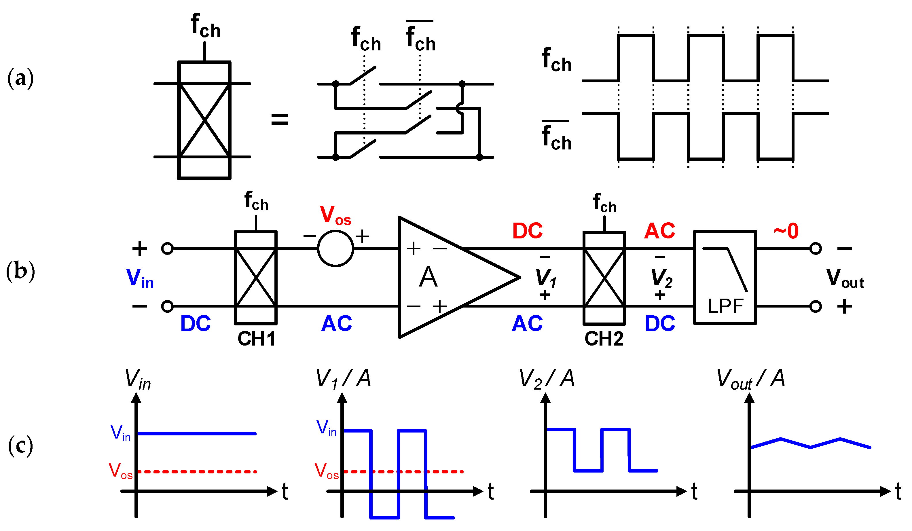
For resistive-bridge sensor readout, the resistance-to-voltage conversion has an advantage of relatively large dynamic range; however, nonlinear outputs, due to the effects of noise and the nonzero offset by the readout circuit, can occur. To minimize those nonlinearity error components, a precise sensor readout circuit, with low noise and offset, is required. The chopper stabilization scheme can reduce low-frequency noises, achieving the required low-noise specification [9]. Figure 2 shows the well-known chopping principle, with chopped amplifier and its ideal time domain waveforms. The input voltage in the DC band, Vin, is modulated by a chopper CH1, with clock frequency fch, and it is converted to a modulated AC signal. Next, the modulated AC signal and input offset are amplified together with amplifier gain, A. Then the output chopper, CH2, demodulates the amplified AC modulated signal back to DC signal. The offset to the odd harmonics of fch, modulated by the CH2, can be filtered out after passing the LPF. Thus, the thermal-noise limited signal-to-noise ratio (SNR) can be achieved.
In this paper, we propose a low-noise, low-power, and high-input impedance readout IC for resistive microsensors. To overcome the power–noise tradeoff, the chopper-stabilized, current-feedback instrumentation amplifier (CFIA), with RFC topology, is proposed. High-current, efficient operational transconductance amplifier (OTA) using RFC topologies have been extensively investigated; however, CFIA using RFC topologies, which has two input differential pairs and acts as differential difference amplifier, are rarely considered. To the author’s best knowledge, CFIA based on RFC has not been reported. The chopper stabilization technique is an effective way to reduce low-frequency noise and is widely used in various instrumentation amplifiers. The RFC topology can reduce power consumption under the same desired bandwidth. Moreover, the high-input impedance with the tens femtofarads of small gate capacitance can be achieved with the proposed IA scheme.
This paper consists of the following order. In Section 2, the proposed resistive-bridge sensor ROIC with chopper-stabilized RFC CFIA is explained with simulation results. Section 3 describes experimental results and summarized performance of the proposed ROIC. Additional discussion and conclusions are presented in Section 4.

2. Proposed Resistive-Bridge Readout Integrated Circuit

This section discusses a proposed low-power and low-noise resistive-bridge microsensor ROIC with chopper-stabilized RFC IA. Section 2.1 discusses the top architecture and sub-blocks of the proposed resistive-bridge microsensor ROIC. Section 2.2 explains the schematic and operating principles of a chopper-stabilized RFC IA. Section 2.3 explains the AOCL, LPF, ADC driving buffer, and 12-bit SAR ADC, briefly.

2.1. Top Architecture of the Proposed Resistive-Bridge Microsensor ROIC

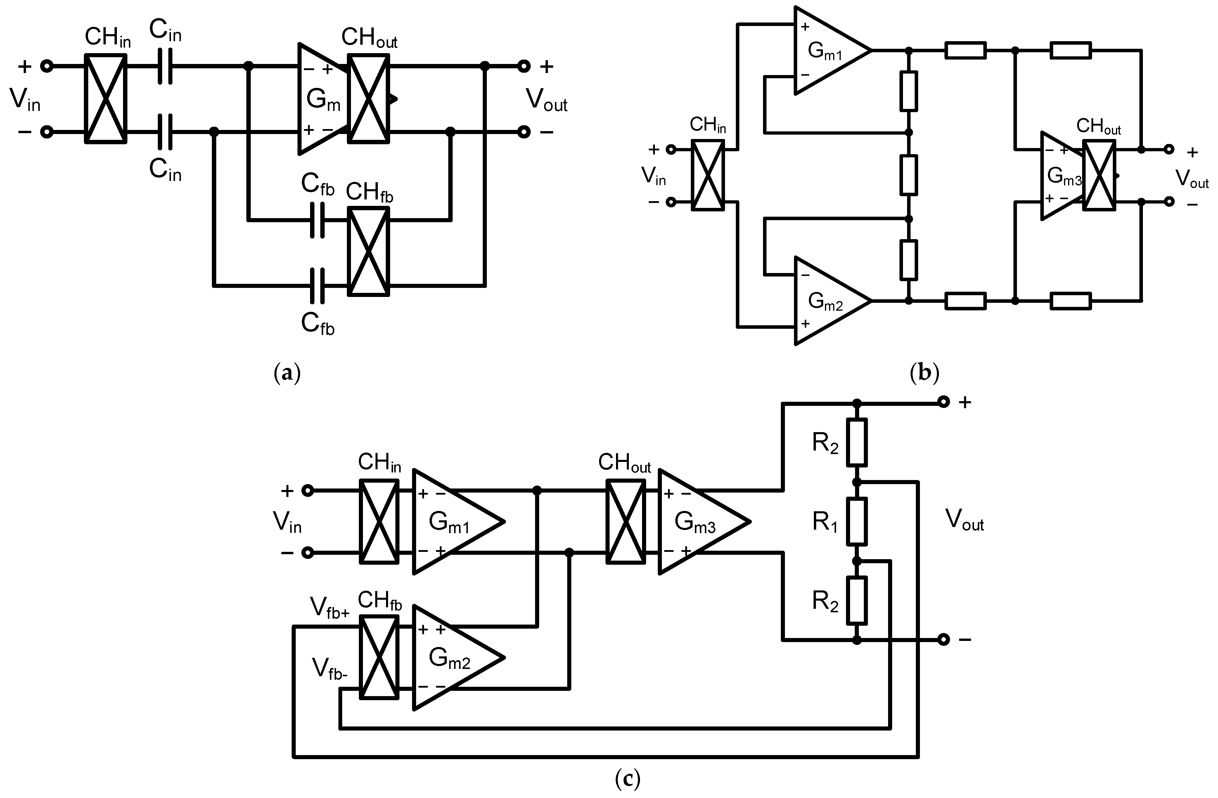
Three types of the IAs are mainly utilized: the capacitively-coupled, conventional 3-opamp, and current feedback IAs. To prevent signal distortion, high-input impedance is an important parameter. In Figure 3a, showing the capacitive-coupled instrumentation amplifier (CCIA) scheme, the input impedance at the input node of the amplifier is reduced, owing to the shunt–shunt feedback. The input impedance of the CCIA can be expressed as:
Z I N ( C C I A ) = | 2 s C i n | = | 2 2 π f C H C i n |
Its input impedance is typically in the order from several hundred kΩ to several MΩ, determined by the impedance of the input capacitors and the chopping frequency. To increase the input impedance, the input impedance boosting schemes, using positive feedback or input pre-charge techniques, are used; however, the complexity of the stability and circuits are drawbacks [10,11]. As shown in Figure 3b,c, the 3-opamp IA and the CFIA receive input signals directly from the gate input node of the amplifier, and only the small gate input capacitances are only shown at the input node; thus, much higher input impedance can be achieved than with the CCIA.
The input impedance of the 3-opamp IA and CFIA can be expressed as (4):
Z I N ( 3 o p a m p , C F I A ) = | 2 s C g | = | 2 2 π f C H C g |
where Cg is the gate input capacitance of input transconductance, Gm1. In this design, the gate capacitance, Cg, is simulated to 272.8 fF, which is total gate capacitance (cgg). From the power consumption perspective, the CFIA is more efficient than 3-opamp IA because the output stages are shared. Moreover, by converting the input differential voltage signal through the input transconductance, Gm1, to differential current, the input common-mode and the feedback common-mode can be separated, thus CFIA achieve the higher CMRR, compared to 3-opamp IA [12,13].
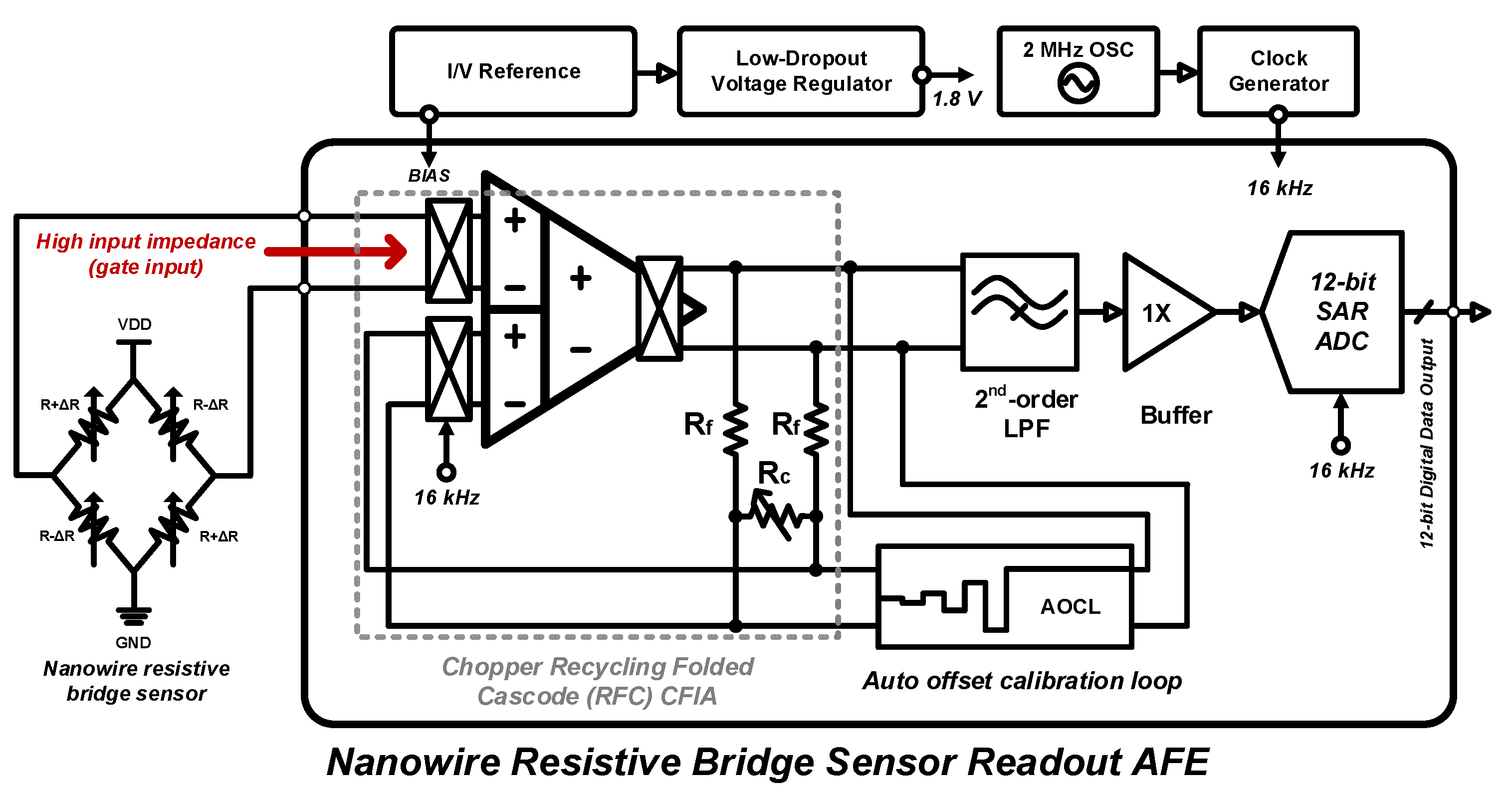
The top block diagram of the proposed resistive-bridge microsensor ROIC is shown in Figure 4. It consists of a chopper-stabilized CFIA, low-pass filter (LPF), ADC driving buffer, and 12-bit successive-approximation-register (SAR) analog-to-digital converter (ADC). First, the resistive sensor converts the resistance to the voltage signal, the input signal is amplified through the first stage (which is the proposed, fully differential CFIA). The gain of proposed CFIA is determined by the feedback resistors Rf and Rc, and the gain can be adjusted to 4-bits (DIN<3:0>) via the programmable resistance, Rc, through the SPI. The gain of the proposed CFIA can be expressed as:
g a i n = 1 + 2 · R f R c
Figure 5 shows the transfer function of the CFIA, in which the gain is adjusted from 70.6 (DIN<3:0> = 1111) to 220.3 (DIN<3:0> = 0000). The amplified signal goes through the 2nd-order LPF, with 500 Hz cutoff frequency and buffer, and finally converts to the digital signal through the 12-bit SAR ADC.

2.2. Circuit Implementation of a Chopper-Stabilized, Recycling Folded Cascode Instrumentaation Amplifier

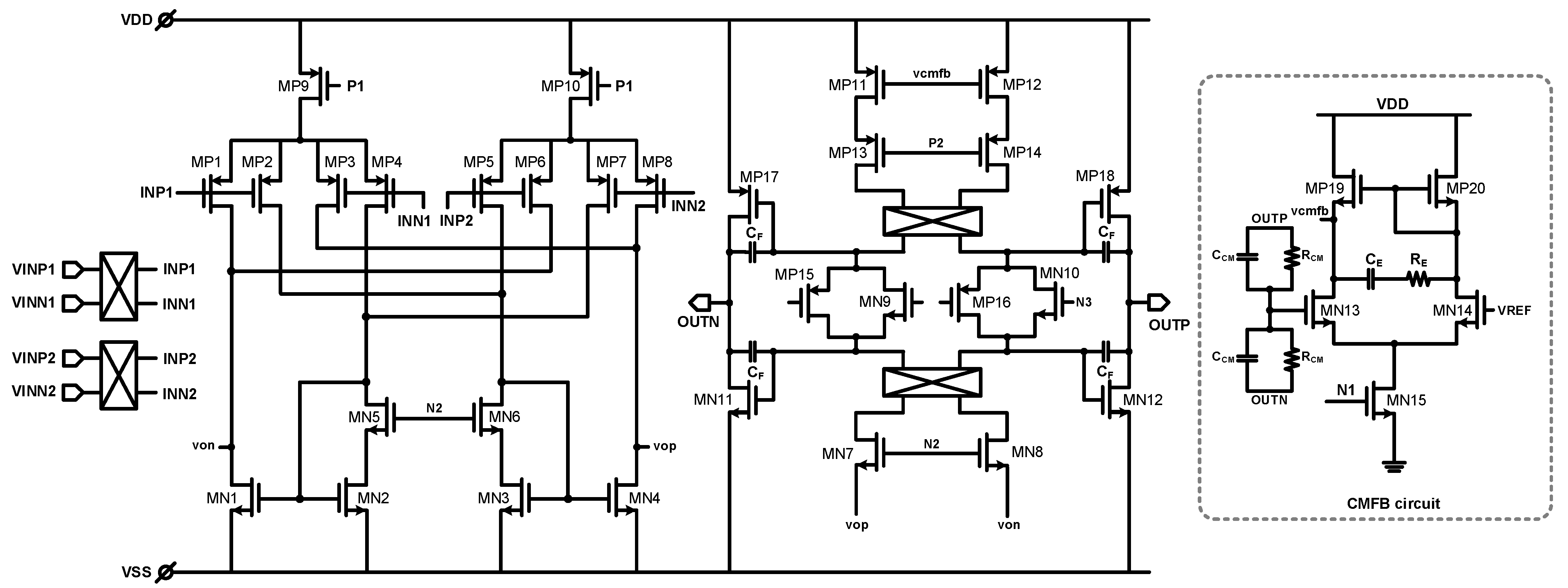
Figure 6 shows the schematic of the proposed chopper-stabilized RFC IA. To reduce low-frequency noise, the choppers are added to the input stage and the folded cascode stage. For using fully differential CFIA topology, the differential difference amplifier (DDA)-style input stages are needed. The PMOS differential pairs, MP1–MP4, form the recycling folded cascode input stage, and MP5–MP8 forms the feedback input stage. MN1–MN4 work as driving transistors, with a ratio of 5:6, as shown in (6).
M N 2 : M N 1 = M N 3 : M N 4 = 5 : 6
The cross-over connections of these current mirrors keep the small-signal input currents added at the sources of MN7 and MN8, in phase. The Monticelli-style, floating class-AB control units are implemented using MP15, MN9, MP16, and MN10. By implementing class-AB output stage, Gm and GBW of the RFC can be increased.
The compensation capacitors, CFs, are connected between the output nodes and gate of the output common source stage in a Miller compensation manner to compensate for the frequency response. The RCMs and CCMs detect the output common-mode voltage. The error amplifier for common-mode feedback consists of MP19, MP20, MN13, MN14, and MN15 to generate the control voltage vcmfb, which controls the bias current of the cascode stages. The W/L values of the transistors and passive components (in the proposed RFC’s fully differential difference amplifier) are shown in Table 1 and Table 2, respectively.
The transconductance of the 1st-stage can be increased by 11/5, according to expression (1) and can be expressed as (7). The gain bandwidth can be determined by the GmRFC and compensation capacitor, CF, as (8).
G m R F C ( 1 s t s t a g e ) = 11 5 g m P M 1 a
G B W R F C = G m R F C 2 π C F
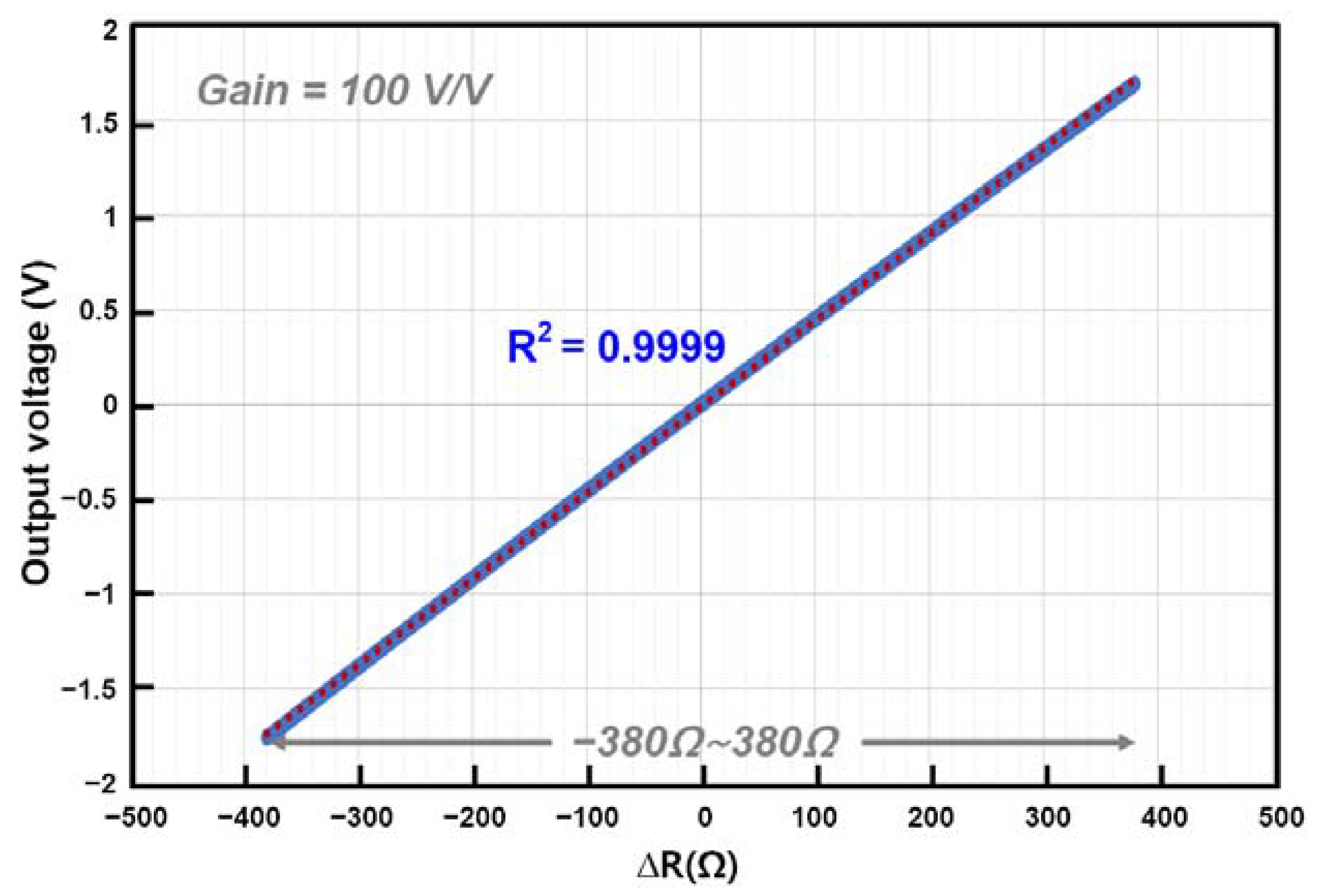
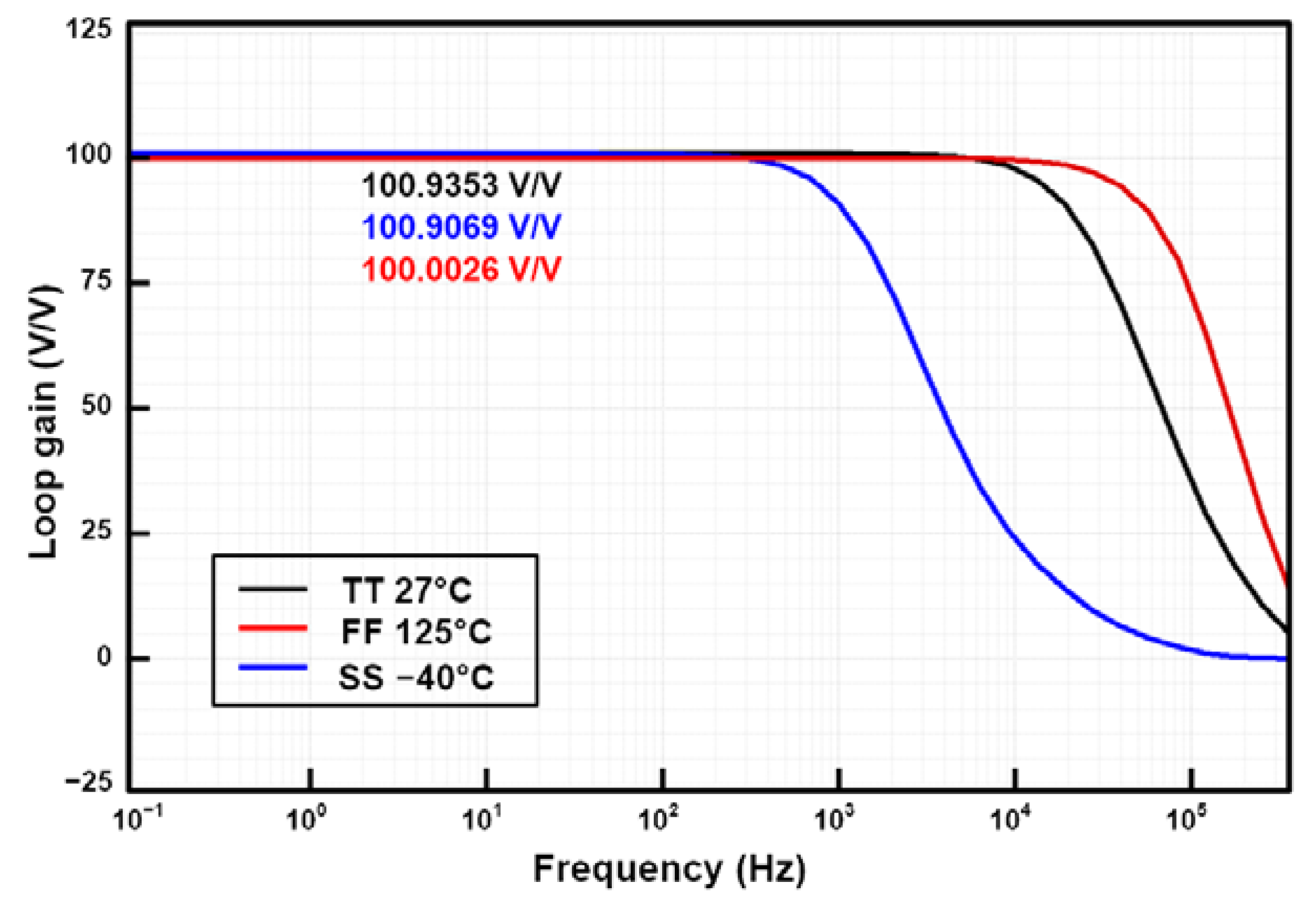
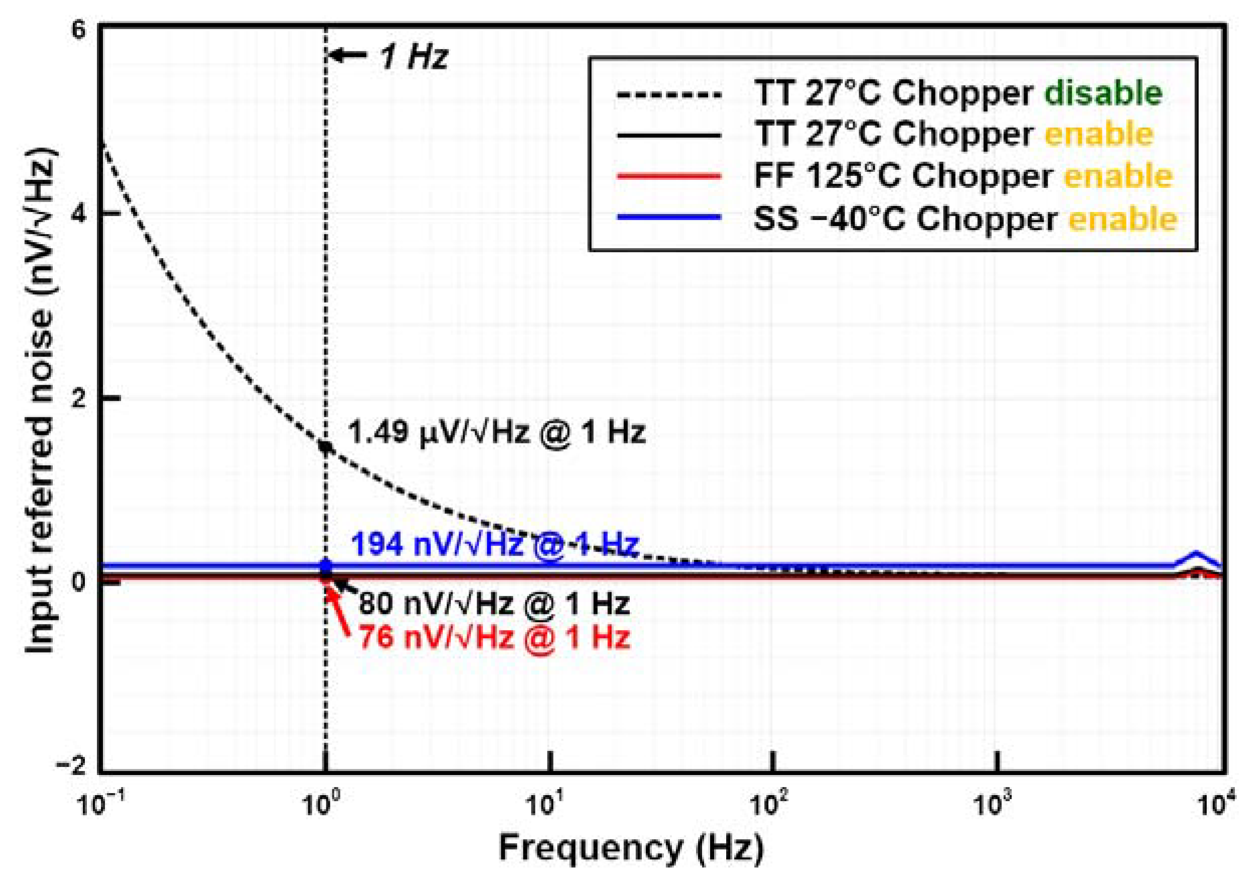
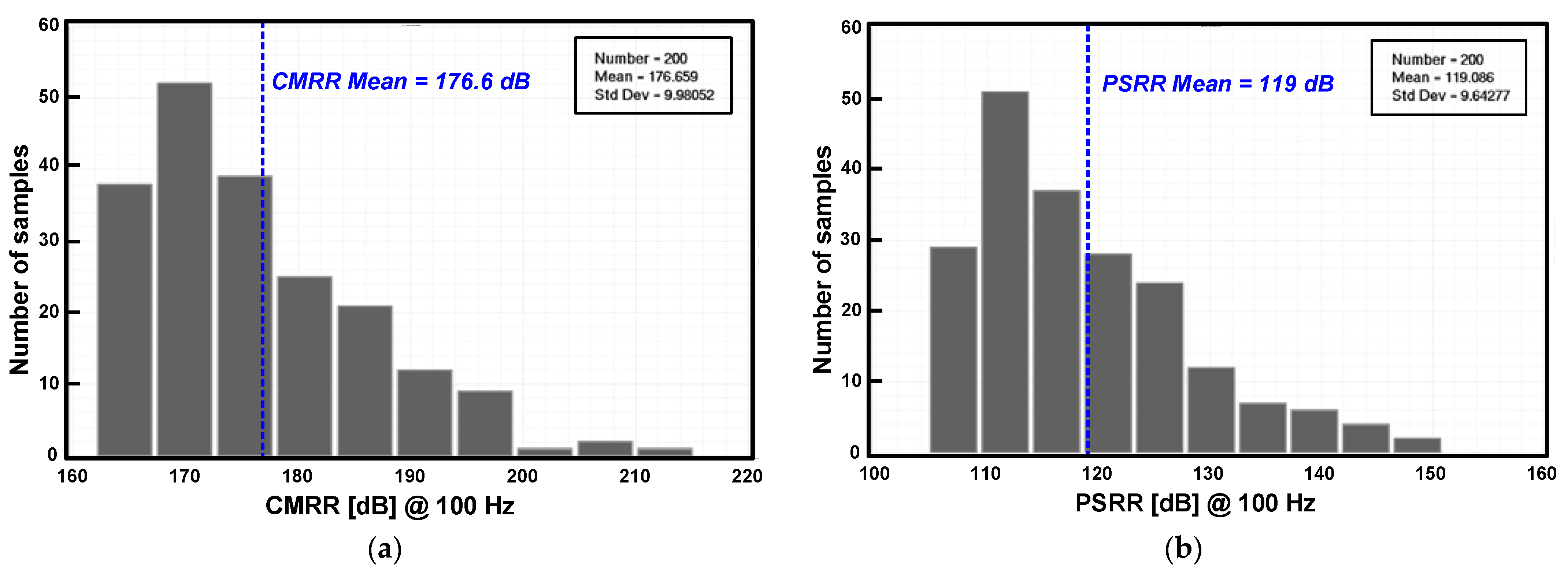
The simulated input–output characteristics of the RFC CFIA are shown in Figure 7. The coefficient of the determination R2 was calculated to be 0.9999, within the resistance variation (∆R) range of −380Ω~380Ω. Figure 8 shows the closed-loop gain of the proposed RFC CFIA, based on corner simulation. The closed-loop gain varies from 100.0026 V/V (at the FF 125 °C) to 100.9353 V/V (at the TT 29 °C). Figure 9 shows the input-referred noise, with corner simulation results, when the chopper is enabled and disabled. The input-referred, low-frequency noise at 1 Hz is reduced from 1.49 µV/√Hz (when the chopper is disabled) to 80 nV/√Hz (TT 27 °C) (when the chopper is enabled). The input-referred noise is reduced to 1/18.6 times with the chopper operation. The corner simulation results of the CMRR and PSRR are shown in Figure 10. The value of the CMRR and PSRR at 100 Hz varies from 237 dB to 267 dB and 165 dB to 199 dB, respectively. With the Monte Carlo simulations, the high CMRR and PSRR were obtained as shown in Figure 11. The mean values of the CMRR and PSRR at 100 Hz, with mismatch, are 176.6 dB and 119 dB, respectively. The simulations were performed with the default feedback gain configuration (DIN<3:0> = 1000, gain = 100 V/V).

2.3. AOCL, LPF, ADC Driving Buffer, and 12-Bit SAR ADC

The proposed CFIA circuit used chopper stabilization techniques for low-noise performance, but the undesired offset of the resistive-bridge sensor also be amplified at the output stage of the CFIA. To solve this problem, we added an automatic offset calibration loop (AOCL) for offset cancellation. The AOCL consists of a comparator, a 12-bit SAR logic block, and a 12-bit R-2R digital-to-analog converter (DAC). When offset is amplified through the CFIA, the output of the CFIA is compared through the comparator input connected to the CFIA output. The output of the comparator passes through the 12-bit SAR logic to generate the corresponding 12-bit digital code and is applied as an input to the 12-bit R-2R DAC, which generates the corresponding compensation voltage to compensate the offset. The low-frequency noise, modulated at the chopper frequency, is shown at the output as a ripple; the 2nd-order 500 Hz LPF was used to remove the chopper ripple. The signal amplified through the IA is converted to the digital signal through the 12-bit SAR ADC, after ADC buffer. The detailed circuit implementations of the 500 Hz 2nd-order LPF, buffers for driving ADC, 12-bit SAR ADC, and AOCL are described in [14,15,16,17].

3. Experimental Results

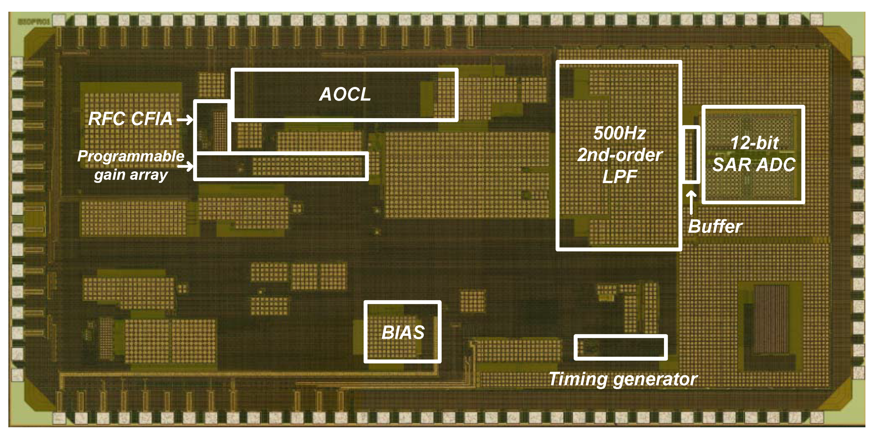
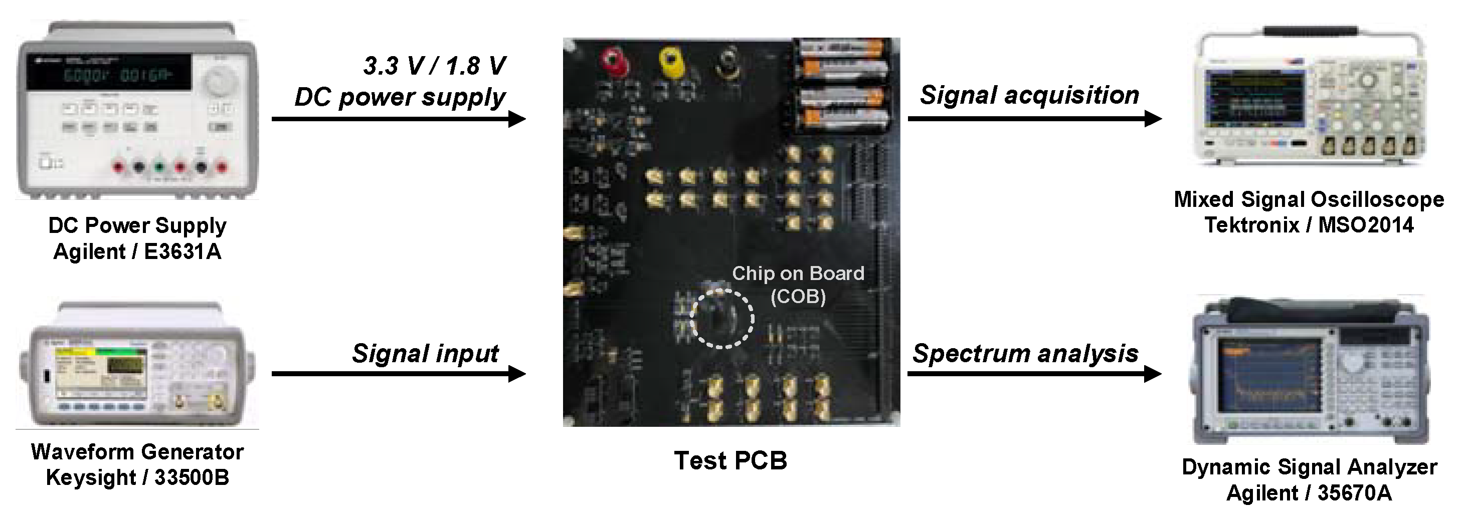
Figure 12 shows the die photograph of the proposed resistive-bridge readout IC. The IC is fabricated using a TSMC 180 nm CMOS process, resulting in the RFC CFIA block size of 293 µm × 183 µm. The printed circuit board (PCB) was designed to evaluate the performance of the proposed IC, the test board and the measurement environment are shown in Figure 13.
Figure 14 shows the voltage output of the IC, which varies along the pressure applied to the resistive strain gauge force sensor, which has 10 kOhm flat resistance; the resistance varies from 14 kΩ to 26 kΩ [18]. Figure 15a shows the measured transient response when the input source is a 5 mVpp differential sine wave input. Figure 15b shows the measured transfer function of the CFIA when the gain setting is maximum (<DIN> = 0000), resulting in 46.12 dB DC gain and 580 kHz unit gain bandwidth (UGBW).
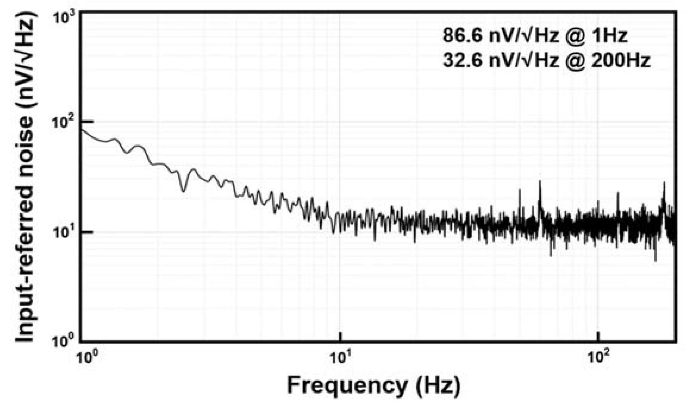
The measured input-referred noise is 86.6 nV/√Hz at 1 Hz and 32.6 nV/√Hz at 200 Hz, as shown in Figure 16. The minimum current consumption of the IC is 3 μA (where only IA and bias block are used and if the LPF, buffer, ADC, and timing generator are fully utilized) the power consumption is 7.954 μA. The noise-efficiency-factor (NEF) is widely used to compare the power–noise trade-offs [19]. The NEF can be calculated by (9).
N E F = V n i , R M S · 2 · I t o t π · U T · 4 k T · B W
The NEF value is proportional to the input reference noise of the IA and the current consumption, which can be used to determine whether IA with low NEF has performance advantages. The NEF of the proposed IA is calculated to be 4.94. The performance comparisons of the proposed circuit, with the previous works regarding resistive-bridge ROIC, are summarized in Table 3.

4. Discussion and Conclusions

In this paper, a low-power, low-noise, resistive-bridge microsensor readout circuit with chopper-stabilized, recycling folded cascode instrumentation amplifier is presented. The readout circuit consists of a chopper-stabilized RFC IA, AOCL, 2nd-order LPF, ADC driving buffer, and 12-bit SAR ADC. The RFC structure was used to achieve low-power consumption. Additionally, low-noise was implemented by applying the chopper stabilization technique, and to realize high-input impedance for accurate signal amplifying, CFIA topology was implemented. The proposed readout circuit was implemented in a standard 0.18 µm CMOS process, with an active area of 12.5 mm2. The measured input-referred noise at 1 Hz was 86.6 nV/√Hz and the noise efficiency factor (NEF) was 4.94, respectively. The total current consumption was 2.23 μA, with a 1.8 V power supply. There were trade-offs between the input-referred noise and power consumption. The input-referred noise in this paper was higher; however, the power consumptions were lower than the previous research (in Table 3). This chip achieves relatively lower NEF, which shows the power–noise efficiency. The gain of the proposed IA can be adjusted from 70 to 220, via a 4-bit programmable resistor array DIN<3:0>, so that it can be expected to be available for various resistive-bridge sensor applications.

Author Contributions

Conceptualization and supervision, H.K. (Hyoungho Ko); investigation and writing—original draft preparation, G.C.; writing—review and editing, H.H., D.Y., H.K. (Hyungseup Kim), K.N., M.Y. and S.L. All authors have read and agreed to the published version of the manuscript.

Funding

This research was supported by the Practical Technology Development Medical Microrobot Program (R&D Center for Practical Medical Microrobot Platform, HI19C0642), funded by the Ministry of Health and Welfare (MOHW, Korea) and the Korea Health Industry Development Institute (KHIDI, Korea).

Institutional Review Board Statement

Not applicable.

Informed Consent Statement

Not applicable.

Data Availability Statement

Not applicable.

Acknowledgments

The EDA tool was supported by the IC Design Education Center (IDEC), Korea.

Conflicts of Interest

The authors declare no conflict of interest.

References

  1. Vetrivel, S.; Mathew, R.; Sankar, A.R. Design and optimization of a doubly clamped piezoresistive acceleration sensor with an integrated silicon nanowire piezoresistor. Microsyst. Technol. 2016, 23, 3525–3536. [Google Scholar] [CrossRef]
  2. Zhang, Y.; Zhang, Z.; Pang, B.; Yuan, L.; Ren, T. Tiny MEMS-based pressure sensors in the measurement of Intracranial Pressure. Tsinghua Sci. Technol. 2014, 19, 161–167. [Google Scholar] [CrossRef]
  3. Zhang, X.; Maddipatla, D.; Bose, A.K.; Hajian, S.; Narakathu, B.B.; Williams, J.D.; Mitchell, M.F.; Atashbar, M.Z. Printed Carbon Nanotubes-Based Flexible Resistive Humidity Sensor. IEEE Sens. J. 2020, 20, 12592–12601. [Google Scholar] [CrossRef]
  4. Lee, J.-H.; Yeh, S.-K.; Fang, W. Vertically Integrated Double-Bridge Design for CMOS-MEMS Tri-Axial Piezo-Resistive Force Sensor. In Proceedings of the 2020 IEEE 33rd International Conference on Micro Electro Mechanical Systems (MEMS), Vancouver, BC, Canada, 18–22 January 2020; pp. 693–696. [Google Scholar]
  5. Assaad, R.S.; Silva-Martinez, J. The Recycling Folded Cascode: A General Enhancement of the Folded Cascode Amplifier. IEEE J. Solid-State Circuits 2009, 44, 2535–2542. [Google Scholar] [CrossRef]
  6. Algueta-Miguel, J.M.; Lopez-Martin, A.; Garde, M.P.; De La Cruz, C.A.; Ramirez-Angulo, J. ±0.5 V 15 μ W Recycling Folded Cascode Amplifier With 34767 MHz·pF/mA FOM. IEEE Solid-State Circuits Lett. 2018, 1, 170–173. [Google Scholar] [CrossRef]
  7. Akbari, M.; Hashemipour, O.; Javid, A. An ultra-low voltage, ultra-low power fully recycling folded cascode amplifier. In Proceedings of the 2014 22nd Iranian Conference on Electrical Engineering (ICEE), Tehran, Iran, 20–22 May 2014; pp. 514–518. [Google Scholar]
  8. Sarkar, A.; Panda, S.S. Design of a power efficient, high slew rate and gain boosted improved recycling folded cascode amplifier with adaptive biasing technique. Microsyst. Technol. 2017, 23, 4255–4262. [Google Scholar] [CrossRef]
  9. Wu, R.; Huijsing, J.H.; Makinwa, K.A. Precision Instrumentation Amplifiers and Read-Out Integrated Circuits; Springer: New York, NY, USA, 2012; pp. 28–29. [Google Scholar]
  10. Jiang, H.; Nihtianov, S.; Makinwa, K.A.A. An Energy-Efficient 3.7-nV/√Hz Hz Bridge Readout IC With a Stable Bridge Offset Compensation Scheme. IEEE J. Solid-State Circuits 2018, 54, 856–864. [Google Scholar] [CrossRef] [Green Version]
  11. Pham, X.T.; Duong, D.N.; Nguyen, N.T.; Van Truong, N.; Lee, J.-W. A 4.5 GΩ-Input Impedance Chopper Amplifier with Embedded DC-Servo and Ripple Reduction Loops for Impedance Boosting to Sub-Hz. IEEE Trans. Circuits Syst. II Express Briefs 2021, 68, 116–120. [Google Scholar] [CrossRef]
  12. Witte, J.F.; Huijsing, J.H.; Makinwa, K.A.A. A Chopper and Auto-Zero Offset-Stabilized CMOS Instrumentation Amplifier. In Proceedings of the 2009 Symposium on VLSI Circuits, Kyoto, Japan, 16–18 June 2009; pp. 210–211. [Google Scholar]
  13. Dool, B.V.D.; Huijsing, J. Indirect current feedback instrumentation amplifier with a common-mode input range that includes the negative roll. IEEE J. Solid-State Circuits 1993, 28, 743–749. [Google Scholar] [CrossRef] [Green Version]
  14. Song, H.; Park, Y.; Kim, H.; Cho, D.-I.D.; Ko, H. Fully Integrated Low-Noise Readout Circuit with Automatic Offset Cancellation Loop for Capacitive Microsensors. Sensors 2015, 15, 26009–26017. [Google Scholar] [CrossRef] [PubMed] [Green Version]
  15. Nam, K.; Kim, H.; Kwon, Y.; Choi, G.; Kim, T.; Kim, C.; Cho, D.; Lee, J.; Ko, H. A Four-Channel Low-Noise Readout IC for Air Flow Measurement Using Hot Wire Anemometer in 0.18 μm CMOS Technology. Sensors 2021, 21, 4694. [Google Scholar] [CrossRef] [PubMed]
  16. Lee, B.; Kim, H.; Kim, J.; Han, K.; Cho, D.-I.D.; Ko, H. A low-power 33 pJ/conversion-step 12-bit SAR resistance-to-digital converter for microsensors. Microsyst. Technol. 2018, 25, 2093–2098. [Google Scholar] [CrossRef]
  17. Kwon, Y.; Kim, H.; Kim, J.; Han, K.; You, D.; Heo, H.; Cho, D.-I.; Ko, H. Fully Differential Chopper-Stabilized Multipath Current-Feedback Instrumentation Amplifier with R-2R DAC Offset Adjustment for Resistive Bridge Sensors. Appl. Sci. 2019, 10, 63. [Google Scholar] [CrossRef] [Green Version]
  18. Resistive Flex Sensors, Spectrasymbol. Available online: https://www.spectrasymbol.com/product/flex-sensors (accessed on 28 August 2021).
  19. Steyaert, M.S.J.; Sansen, W.M.C. A micropower low-noise monolithic instrumentation amplifier for medical purposes. IEEE J. Solid-State Circuits 1987, 22, 1163–1168. [Google Scholar] [CrossRef]
  20. Xie, P.; Duan, Q.; Meng, Z.; Huang, S.; Ding, Y.; Han, L. A Low-Noise, Low-Power, and Chopper-Stabilized, Cur-rent-Feedback Instrumentation Amplifier for Current Sensing Application. In Proceedings of the 2019 IEEE 4th International Conference on Integrated Circuits and Microsystems (ICICM), Beijing, China, 25–27 October 2019; pp. 162–165. [Google Scholar]
  21. Jun, J.; Rhee, C.; Kim, M.; Kang, J.; Kim, S. A 21.8 b Sub-100 μHz 1/f Corner 2.4μV-Offset Programmable-Gain Read-out IC for Bridge Measurement Systems. In Proceedings of the 2018 IEEE International Solid-State Circuits Conference (ISSCC), San Francisco, CA, USA, 11–15 February 2018; pp. 330–332. [Google Scholar]
  22. Jiang, H.; Makinwa, K.A.A.; Nihitanov, S. An energy-efficient readout method for piezoresistive differential pressure sensors. In Proceedings of the IECON 2017—43rd Annual Conference of the IEEE Industrial Electronics Society, Beijing, China, 29 October–1 November 2017; pp. 4287–4291. [Google Scholar]
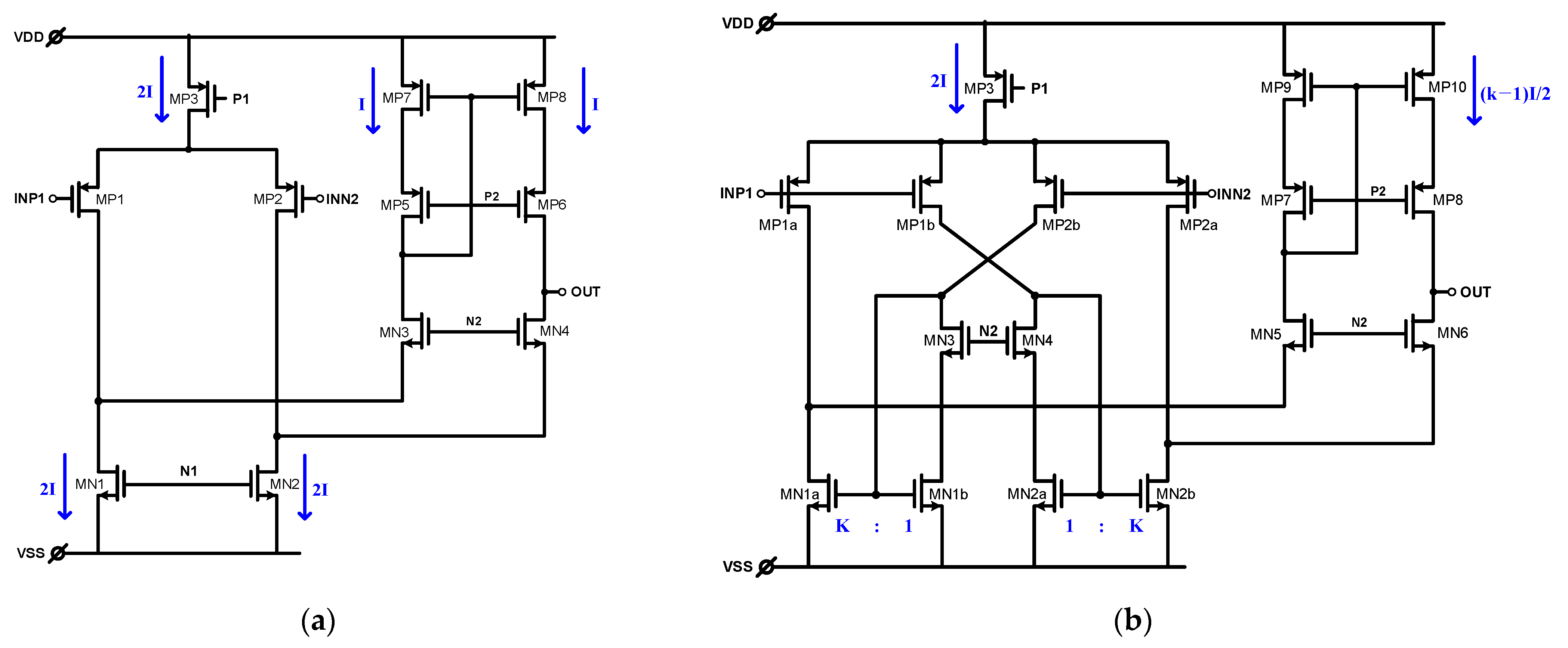
Figure 1. (a) conventional folded cascode; (b) recycling folded cascode.
Applsci 11 07982 g001
Figure 2. Chopping principle in the time domain (a) chopper; (b) amplifier with chopper; (c) ideal time domain signal waveforms. Adapted from [9].
Applsci 11 07982 g002
Figure 3. (a) Instrumentation amplifier topologies: (a) block diagram of CCIA; (b) 3-operational amplifier IA; (c) block diagram of a CFIA.
Applsci 11 07982 g003
Figure 4. Top block diagram of the proposed resistive-bridge microsensor readout IC.
Applsci 11 07982 g004
Figure 5. Simulated transfer function of the proposed CFIA.
Applsci 11 07982 g005
Figure 6. Schematic of the proposed chopper-stabilized RFC.
Applsci 11 07982 g006
Figure 7. Simulated input–output characteristics.
Applsci 11 07982 g007
Figure 8. Corner simulation result of the closed-loop gain.
Applsci 11 07982 g008
Figure 9. Simulated result of the input-referred noise.
Applsci 11 07982 g009
Figure 10. Corner simulation results of the (a) CMRR and (b) PSRR.
Applsci 11 07982 g010
Figure 11. Monte Carlo simulation results of the (a) CMRR and (b) PSRR.
Applsci 11 07982 g011
Figure 12. Die photograph of the proposed resistive-bridge readout IC.
Applsci 11 07982 g012
Figure 13. Measurement environment of the proposed IC with test board.
Applsci 11 07982 g013
Figure 14. Measured voltage output response, due to pressure changes of the force sensor.
Applsci 11 07982 g014
Figure 15. (a) Measured transient response (b) Transfer function of the proposed CFIA at the maximum gain.
Applsci 11 07982 g015
Figure 16. Measured input-referred noise.
Applsci 11 07982 g016
Table 1. Values of transistors in proposed RFC FDDA.
TransistorSize (W/L) (μm)TransistorSize (W/L) (μm)
MP1–MP832/4MN1, MN40.6/10
MP9, MP102/1.5MN2, MN30.5/10
MP11, MP124/10MN5, MN68/1
MP13, MP144/10MN7, MN840/12
MP15, MP161/10MN9, MN101/18
MP17, MP182/10MN11, MN121/10
MP19, MP202/2MN13, MN141/16
--MN150.5/12
Table 2. Values of passive components in proposed RFC FDDA.
ComponentValue
CF200 fF
CE16.6 pF
RE466 kΩ
CCM400 fF
RCM11 MΩ
Table 3. Performance summary of proposed resistive-bridge ROIC and comparison with other studies.
This Work[20][13][21][22]
ArchitectureCFIA (with RFC) + choppingCFIA + chopping + RRLCCIA + choppingCCIA + chopping + CDS + RRLRC + chopping
Technology (µm)0.180.180.180.130.35
Supply voltage (V)1.83.31.835
Total current consumption (µA)7.92001200326860
Gain of IA70–2201004016–32-
Gain bandwidth (Hz)580 k---2 k
Current consumption of IA (µA)2.23---700
Input-referred noise (nV/√Hz)86.6233.7164.2
NEF4.946.15.011.14.7
Publisher’s Note: MDPI stays neutral with regard to jurisdictional claims in published maps and institutional affiliations.