Abstract
With the development of 3D integrated packaging technology, failure analysis is facing more and more challenges. Defect localization in a 3D package is a key step of failure analysis. The complex structure and materials of 3D package devices demand non-destructive defect localization technology for full packages. Magnetic field imaging and three-dimensional X-ray technology are not affected by package material or form. They are effective methods to realize defect localization on 3D packages. In this paper, magnetic field imaging and high-resolution three-dimensional X-ray microscopy were used to localize the open defect in a 3D package with a TSV daisy chain. A two-probe RF method in magnetic field imaging was performed to resolve isolation of the defect difficulties resulting from many different branches of TSV daisy chains. Additionally, a linear decay method was used to target sub-micron resolution at a long working distance. Multiple partition scans from a high-resolution 3D X-ray microscopy with a two-stage magnification structure were used to achieve sub-micron resolution. The open location identified by magnetic field imaging was consistent with that identified by a three-dimensional X-ray microscope. The opening was located on the top metal in the proximity of the fifth via. Physical failure analysis revealed the presence of a crack in the top metal at the opening location.
1. Introduction
Recently, with the rapid development of the integrated circuit industry, two-dimensional packaging technology has been unable to meet the increasing requirements for chip performance and packaging density [1]. Therefore, in order to continue Moore’s Law, the development of two-dimensional integrated circuits to three-dimensional integrated circuits is inevitable [2]. TSV interconnect technology is recognized as one of the most promising technologies for 3D packaging [3]. TSV is connected to micro-bumps through a redistribution line (RDL) [4]. Reliable interconnection is the prerequisite and guarantee for high-quality 3D integration [5]. The tiny scale and layered structure of 3D TSV packages make defect detection and failure analysis extremely complex and challenging [6,7,8,9].
Magnetic field imaging and three-dimensional X-RAY technology are not affected by package material or form [10,11], and they are effective in realizing defect localization on a 3D package [12,13].
Magnetic field imaging (MFI) technology is a non-destructive, non-contact defect localization technology [14]. Different from thermal and optical technology, magnetic field detection is not affected by package materials or package forms [15]. Magnetic fields can be detected after passing through multiple layers of metal, chip or packaging materials. Therefore, sample preparation is not necessary when undergoing defect localization by magnetic field imaging technology, such as decapsulation, depassivation layer, etc. There are two major implementations for MFI: Magnetic Current Imaging (MCI) [16], for locating shorts and leakage, and Space Domain Reflectometry (SDR) [17], for locating open defects. Either Superconducting Quantum Interference Device (SQUID) or Giant Magneto Resistive (GMR) sensors can be used for magnetic field imaging. The magnetic field sensitivity and spatial resolution of the two sensors are different. SQUID is the most sensitive magnetic sensor [18], and it can detect the weak current of fully package devices at a working distance of several hundred microns, but its spatial resolution is low. The magnetic field sensitivity of the GMR sensor is low, but the spatial resolution is high [19]. Generally, the SQUID sensor is first used for overall scanning to obtain the approximate location of defects, and the GMR sensor is used for detailed scanning to obtain high-resolution (sub-micron) imaging. In SDR application, the SQUID sensor can detect an RF (~40 MHz) current forming a standing wave when the trace is open [20]. Possible limitations for the SQUID sensor are mainly lack of resolution. Signals in close proximity may not show up as a result of the cancellation effect when signals run in different directions or the two signals are merged together into a single one when they travel in the same direction. Signals in close proximity may also be artificially separated as a result of the inversion algorithm resolution limitation.
X-ray CT (Computed Tomography) is currently the most advanced X-ray detection technology, with 3D imaging capabilities; thus, it is also called 3D X-ray technology [21]. By eliminating the impact of object overlap on detection, the details of the target of interest can be seen visually from the three-dimensional image made by the 3D X-ray, and a large amount of information of covered defects can be accurately obtained, including structure, size, location and other characteristics [22]. The 3D X-ray microscopy with high resolution and high contrast can effectively detect the defects of 3D packaging devices such as bridges, poor soldering, solder joint cracks, and so on [23].
In microelectronics applications, the extreme resolution is a key limiting factor in the application of X-ray CT technology [24]. A high-resolution 3D X-ray microscopy using a two-stage magnification structure was developed [25]. It is different from traditional CT systems, whose resolution depends on focus size and geometric magnification. First of all, the sample image is geometrically magnified, just like traditional CT systems. The X-rays are then converted to visible light on the detector’s scintillation screen, and the image is then magnified further by the optical system [26]. The dependence on geometric amplification is greatly reduced due to the use of the second-stage optical amplification structure. This results in the significant advantage of providing sub-micron resolution over large working distances, resulting in high resolution for large samples (up to 100 mm in diameter) [27].
The previous researches independently studied the application of one of the techniques of magnetic field imaging and high-resolution three-dimensional X-ray in failure analysis [14,28,29]. Achieving high-resolution in a defect location at long working distances without decapsulation or cutting samples is a current research difficulty [30,31]. In addition, many different branches are proving very difficult to isolate and complicate the identification of the circuit, and therefore, analyze [32]. In this paper, magnetic field imaging and high-resolution three-dimensional X-ray techniques were applied simultaneously to open localization on a 3D TSV package for the first time, which was used to verify the effectiveness of both of them. A two-probe RF method in magnetic field imaging was performed to resolve isolation of the defect difficulties resulting from many different branches of TSV daisy chains. Additionally, a linear decay method was used to target sub-micron resolution at a long working distance. Multiple partition scans by high-resolution 3D X-ray microscopy with a two-stage magnification structure were used to achieve sub-micron resolution too.
This paper is organized as follows: Section 2 describes the test sample. Section 3 demonstrates defect localization on the TSV sample after thermal cycling test by magnetic field imaging and high-resolution three-dimensional X-ray technology. Section 4 verifies the open location by microscopic physical analysis. Finally, a conclusion is wrapped up in Section 5.
2. Test Sample
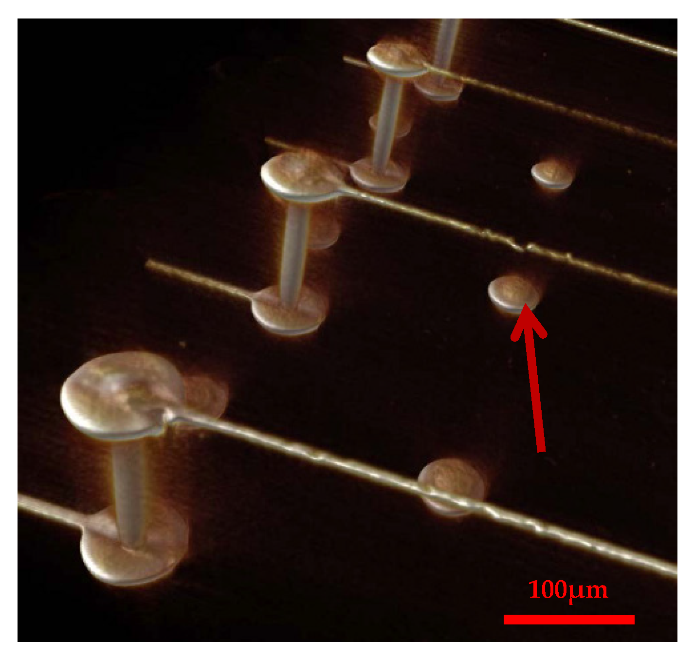
The test sample in this paper contains thirteen groups of TSV daisy chains. Each via is 100 µm deep and 10 µm in diameter, which is filled with copper and with a Ti barrier layer 50 nm thick and a SiO2 dielectric layer 250 nm thick. The TSV connects two metal levels of damascene redistribution copper at the top with one metal level of damascene redistribution copper at the bottom. The vertical structure schematic of each TSV daisy chain unit is as shown in Figure 1. In application, the current is input from the pad of the upper surface metal layer (TOP_M2), travels through the Top_M1 layer, then passes the holes of TSV, down to the lower surface, through the lower surface BTM_M1 layer, then passes the holes of TSV back to the upper surface; it repeats many times, and is finally output from the upper surface.
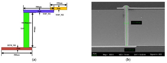
Figure 1.
Vertical structure of TSV daisy chain unit: (a) schematic diagram; (b) SEM image.
After running a thermal cycle experiment from −55 °C to 125 °C on the sample for 1000 cycles, the DC resistance of three groups of TSV daisy chains was increasing significantly. The changes in DC resistance for thirteen groups of TSV daisy chains are shown in Table 1. Channel 6, with the largest resistance change, was selected for analysis.

Table 1.
Changes in DC resistance.
3. Defect Localization
3.1. Magnetic Field Imaging
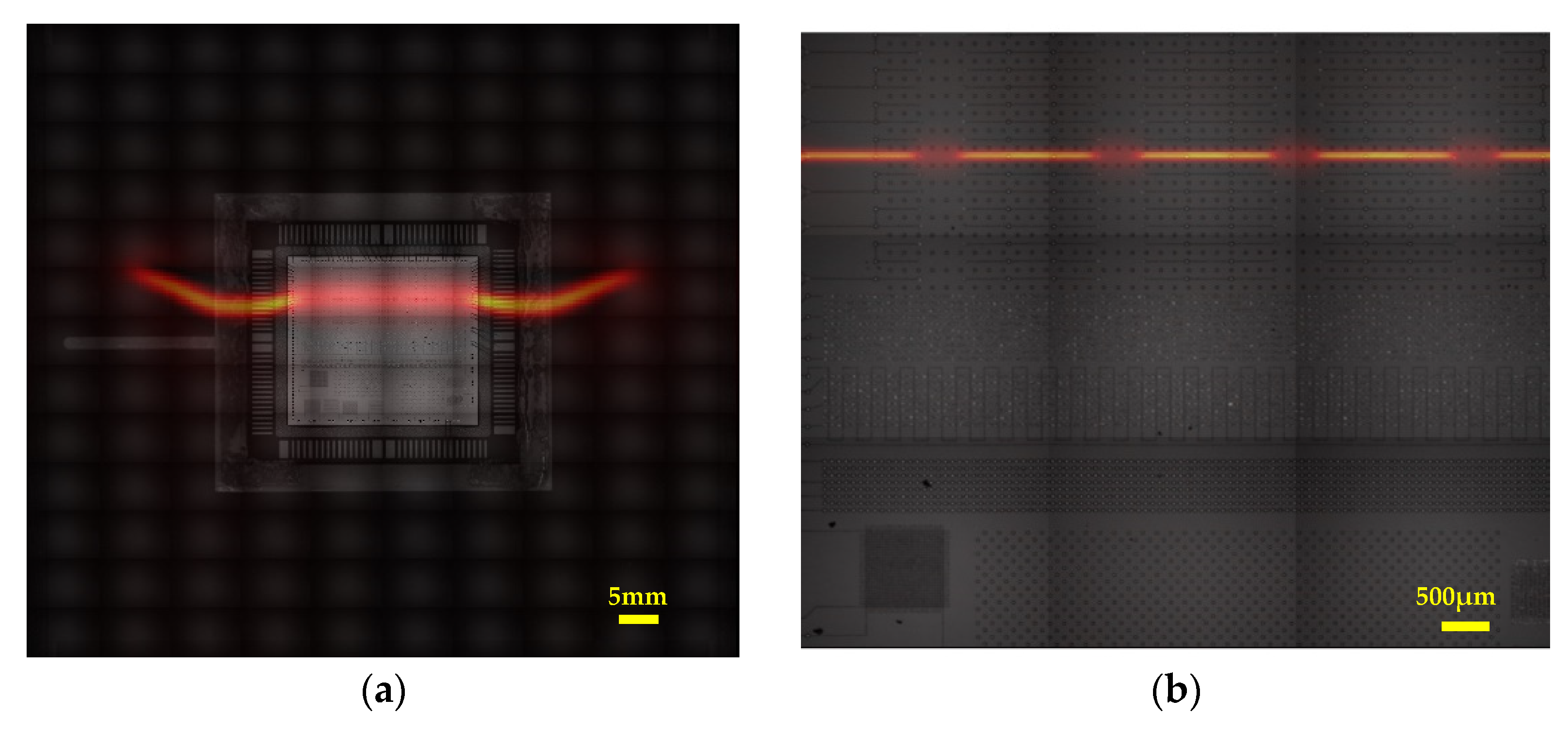
To locate the defect, both fail and reference samples were scanned with the SQUID sensor for an overview scan first and then the GMR sensor for a zoomed-in scan of the die area by Neocera Magma EFI HiRes, as shown in Figure 2 and Figure 3. AC and RF scans were acquired for the reference sample. The AC and RF scans of the reference sample helped us understand the way the current is supposed to propagate in the sample when there is no failure. Only RF scans were acquired for the failing sample. We used a two-probe RF technique for the failing sample to try to isolate the failure channel from the whole grid.
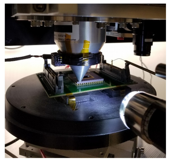
Figure 2.
Failing sample under the SQUID sensor.
Figure 3.
Failing sample under the GMR sensor.
For the AC scan in channel 6, the current input from the pad of upper surface J12 travels through the TOP_M2 layer to the TOP_M1 layer, then passes the TSV down to the lower surface, travels through the BTM_M1 layer, then passes the TSV back to the upper surface, it repeated many times, and finally output from the pad of the upper surface J3. The current image is shown in Figure 4.
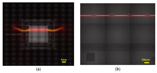
Figure 4.
Overlays of the current images with the optical images: (a) SQUID AC scan; (b) GMR AC scan.
The main circuit path, as shown in the AC scan, shows a weaker signal. The relative intensity of the signal in the fail is lower compared to the reference. The fact that we see a weaker signal in the fail sample points to a possible failure in that path.
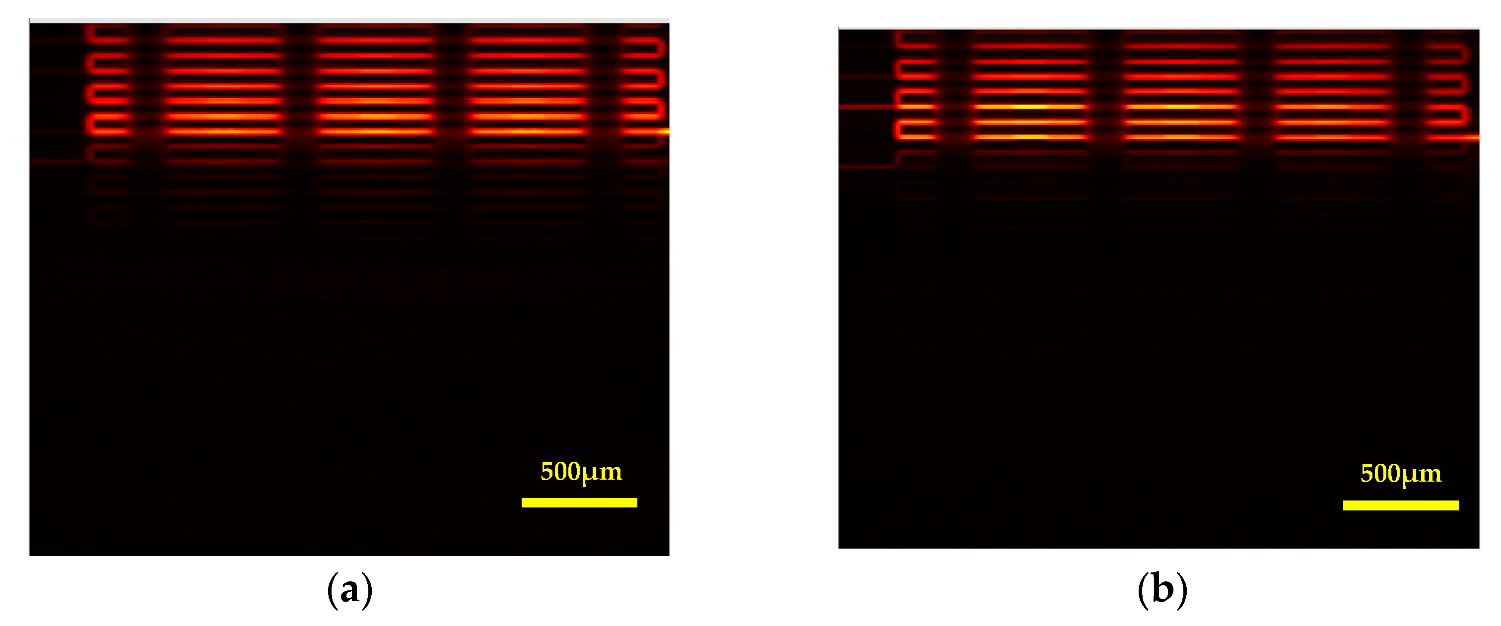
The RF signal followed the whole circuit rather than the single line connecting J12 to J3 in the AC case. For some reason, the RF signal propagated more strongly in the top part of the circuit for both the reference and the fail. This complicated the analysis. The RF scan image from pin J12 on reference and fail sample is shown in Figure 5. The same behavior can be observed from pin J3.

Figure 5.
RF scan from pin J12: (a) Reference sample; (b) Failed sample.
For this reason, a two probe RF technique on pins J3 and J12 was performed. This can help the RF signal to propagate through the path of interest.
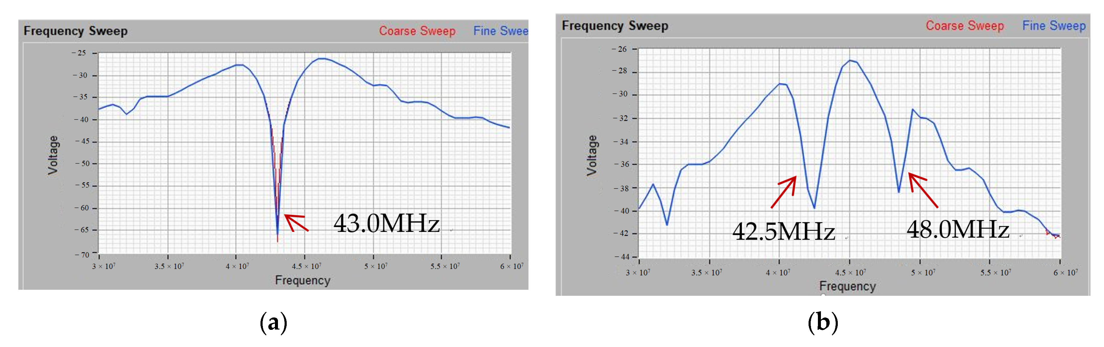
Two RF probes were connected to pins J3 and J12 (Channel 6) at the same time. Some unusual behavior in the frequency sweep for the failing sample was noticed in comparison with the frequency sweep for the reference sample, as shown in Figure 6. The reference sample sweep has only one voltage dip, where the RF signal drops significantly. The failed sample sweep shows two dips at two different frequencies. The typical behavior is to only have a single dip. Scans are performed at different frequencies.

Figure 6.
RF frequency sweep curve: (a) Reference sample; (b) Failed sample.
The reference sample current density data were taken at 43.0 MHz, with one probe on the left side and one probe on the right side. As shown in Figure 7, the signal shows no significant decay along with the green cursor at all three modes.
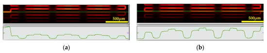
Figure 7.
RF scan on reference sample at 43.0 MHz: (a) Left probe; (b) Right probe.
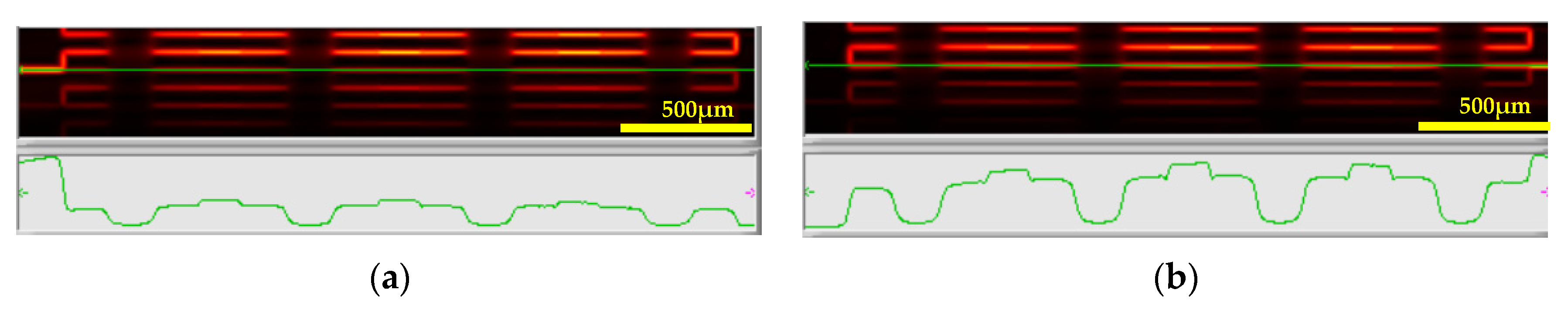
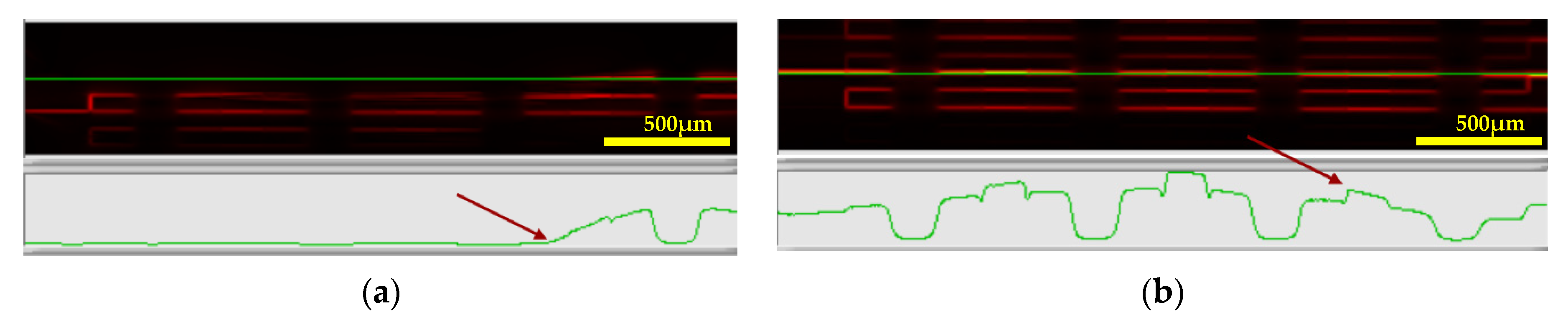
Failed sample current density data were taken with both probes at the same time with two different frequencies, as shown in Figure 8. The signal decays in the same general area for both datasets along the green cursor. The red arrows point to that area of signal decay.
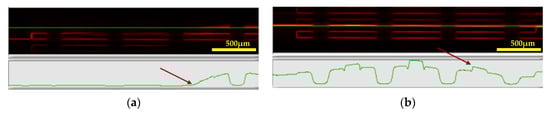
Figure 8.
RF scan with two probes on failed sample: (a) F = 42.5 MHz; (b) F = 48.0 MHz.
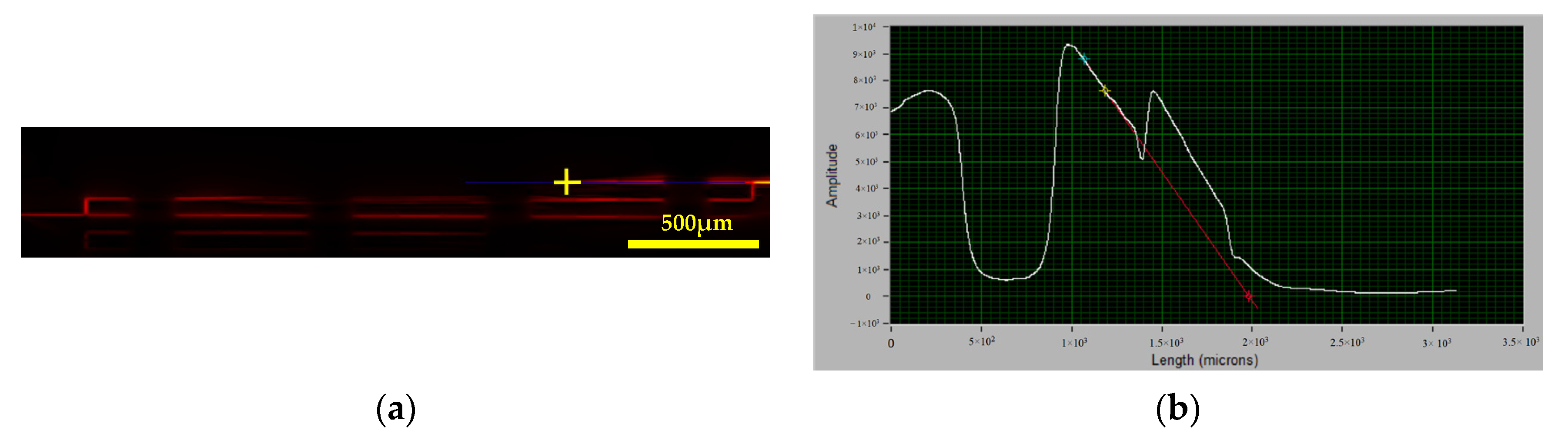
The yellow cross shows the position of the possible open location, as shown in Figure 9 and Figure 10. The linear decay shows us more precisely where the current signal disappears. The linear decay works best with the signals that propagate in one plane. This particular signal seems to changes planes at the same time as it is decaying. We may experience some overshooting from the actual open location. The possible location of the opening was on the right side of the sample in the proximity of the fifth via (see blue arrow in Figure 10). Given the proximity of the location to the via, the fifth via was viewed as the likely opening location.
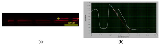
Figure 9.
Possible opening location: (a) Current images; (b) Linear fit position.
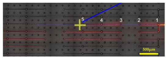
Figure 10.
Optical images overlay with Current images.
3.2. Three-Dimensional X-ray Microscopy
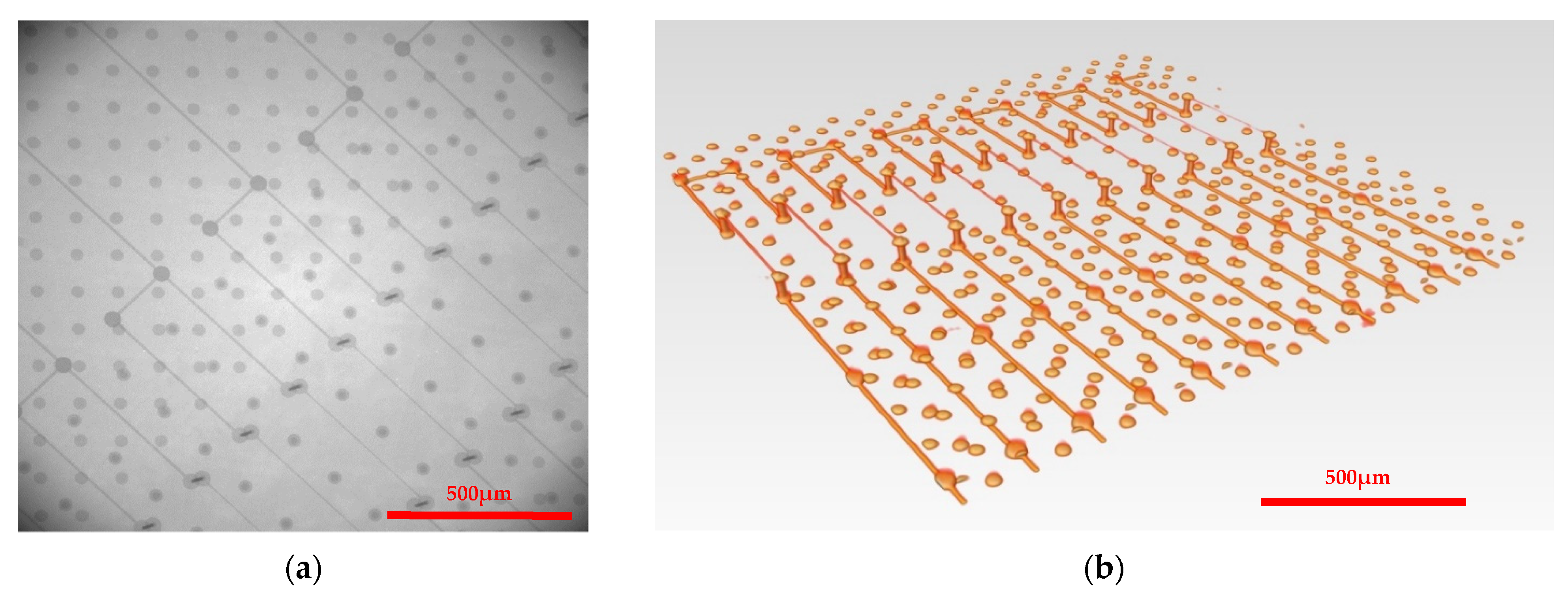
To verify the failure location, the above 3D package with TSV daisy chain was scanned with a high-resolution 3D X-ray microscopy, Zeiss Xradia 510 Versa. The three-dimensional characterization completely displayed the internal structure of the sample, overcame the limitations of the two-dimensional characterization, and combined the high-resolution objective lens to capture the details of the internal structure of the sample to the maximum extent so that the structural characteristics of the TSV array inside the sample could be seen. Two-dimensional X-ray projection image and 3D X-ray reconstruction image of the TSV sample under the overall scan are shown in Figure 11. As shown in this figure, due to the limitation of the resolution, the failure site cannot be observed under the overall scan.

Figure 11.
X-ray image under the overall scan: (a) 2D X-ray projection image; (b) 3D X-ray reconstruction image.
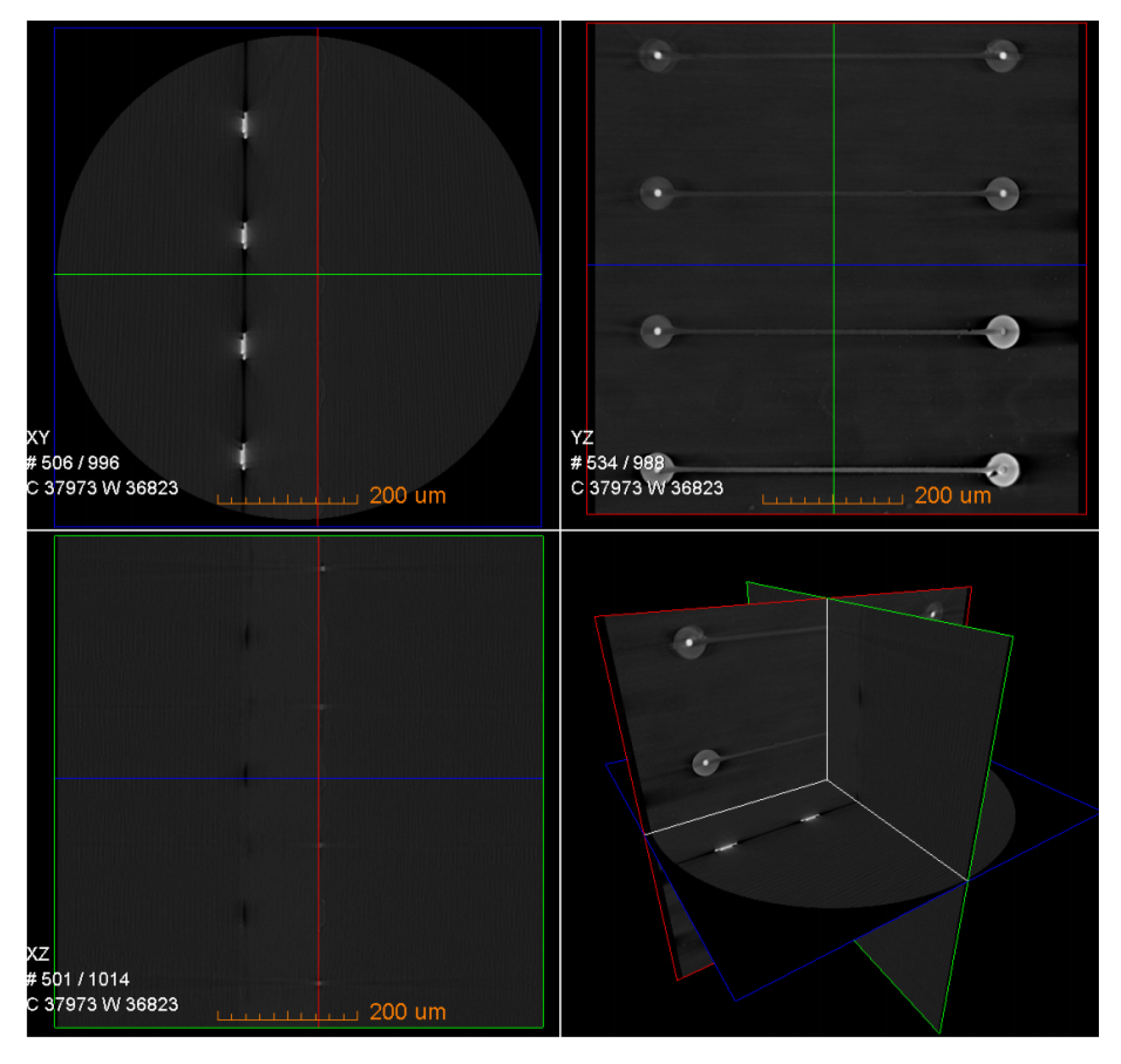
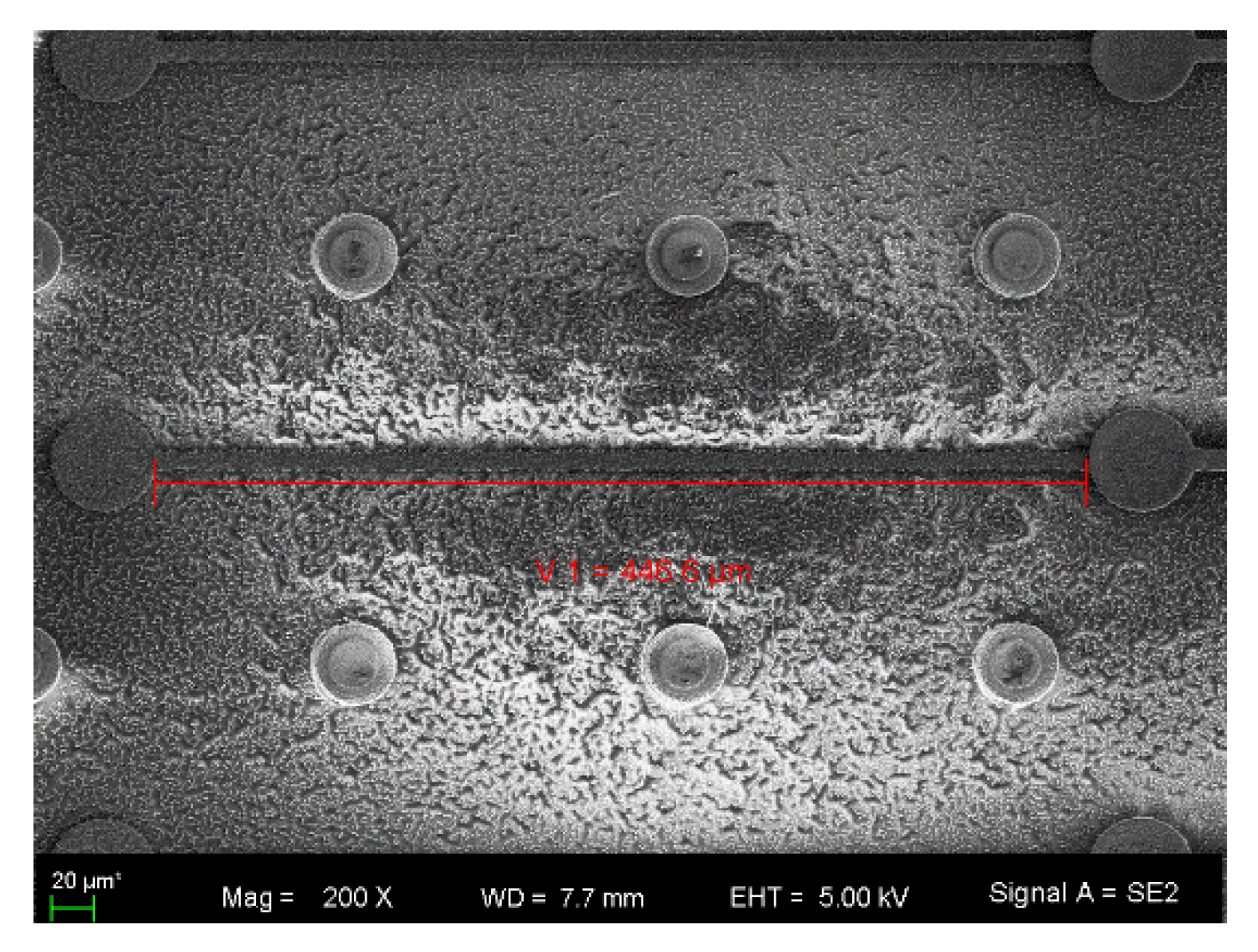
In order to achieve sub-micron resolution, according to the electrical test results, local scanning should be conducted with channel 6 as the center. Due to the long channel, multiple partition scanning is required, followed by image reconstruction and observation, which requires a longer test time. Under the test voltage of 150 kV and the test current of 15 µA, the three-dimensional stereogram, XY section, YZ section and XZ section morphology of the sample in the local magnification scanning are shown in Figure 12. It can be seen that TSV copper columns are arranged neatly and uniformly in thickness, with no voids or cracks. Defects were observed in the Top_M1 layer connecting the two copper pillars. The fracture morphology of the metal layer observed in the XY section is shown in Figure 13. The defect location identified by magnetic field imaging is consistent with three-dimensional X-ray microscopy.
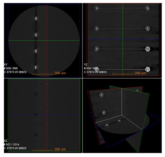
Figure 12.
Three-dimensional stereogram, XY section, YZ section and XZ section morphology in the local magnification scanning.
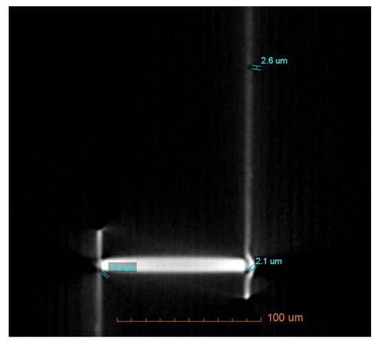
Figure 13.
Fracture morphology of the metal layer observed in XY section.
Figure 14 is the 3D stained image rendered by 3D Viewer software, and the defect structure such as cracks in the sample can be more intuitively observed.

Figure 14.
Three-dimensional stained image rendered using 3D Viewer software.
4. Physical Analysis
To further verify the failure location, decapsulation was performed on the sample, and the surface passivation layer was removed by a reactive ion etcher. No obvious abnormality was observed by metallographic microscopy and scanning electron microscope (SEM) at the position of the open defect localized by magnetic field imaging and 3D XRAY microscopy, as shown in Figure 15 and Figure 16.
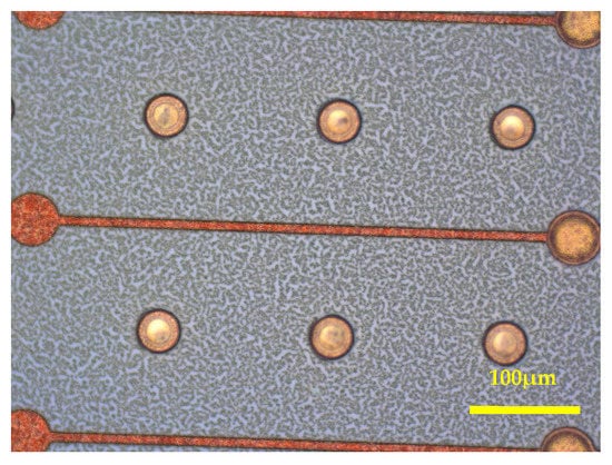
Figure 15.
Morphology under metallographic microscopy.

Figure 16.
Morphology under SEM.
After the surface of the sample was brushed with acid and observed under scanning electron microscopy, the crack defect could be observed at the positions where it is open localized by magnetic field imaging and 3D XRAY microscopy, as shown in Figure 17.
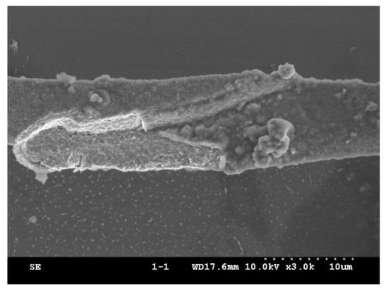
Figure 17.
Crack defect under SEM.
5. Conclusions
State-of-the-art non-destructive defect localization technology, magnetic field imaging and high-resolution three-dimensional X-RAY microscopy were utilized to localize the open defect in a 3D package with a TSV daisy chain in this paper. Open defects were intentionally induced by running a thermal cycle experiment from −55 °C to 125 °C for 1000 cycles. For magnetic field imaging, in order to locate a possible open failure location, it is very important to identify the circuit involved. The AC and RF scans of the reference sample helped us to understand the way that the current is supposed to propagate in the sample when there is no failure. RF signals may show intensity attenuation as they propagate along the circuit and couple to other circuits that are not part of the circuit under study. In this particular case, there were a lot of different branches that proved very difficult to isolate and complicated identification of the circuit. Therefore, a two-probe RF method in magnetic field imaging was performed to resolve isolation of the defect difficulties resulting from many different branches of TSV daisy chains. Moreover, a linear decay method was used to target sub-micron resolution at a long working distance. For three-dimensional X-RAY microscopy, to achieve sub-micron resolution, a high-resolution 3D X-ray microscopy with a two-stage magnification structure was used for scanning. In order to further improve the resolution, multiple partition scans are required, followed by image reconstruction and observation, which requires a long test time. The defect location identified by magnetic field imaging was consistent with that identified by three-dimensional X-ray microscopy. Additionally, the physical failure analysis revealed the presence of a crack in the Top_M1. From the results presented in this paper, it can be concluded that by specific methods, both magnetic field imaging and high-resolution three-dimensional X-RAY imaging can achieve sub-micron resolution in defect location at long working distances without decapsulation or cutting samples. Both technologies are promising for future 3D-architecture-related quality assessment and failure analysis.
Author Contributions
Conceptualization, Y.C. and P.L.; methodology, H.-Z.H.; validation, P.Z. and X.L.; formal analysis, P.Z.; investigation, Y.C.; data curation, Y.C.; writing—original draft preparation, Y.C.; writing—review and editing, H.-Z.H.; funding acquisition, P.L. All authors have read and agreed to the published version of the manuscript.
Funding
This research was funded in part by the Key Realm R&D Program of Guangdong Province under Grant 2018B010142001, in part by the Key Realm R&D Program of Guangdong Province under Grant 2019B010143002 and in part by the Key Realm R&D Program of Guangdong Province under Grant 2019B010145001.
Institutional Review Board Statement
Not applicable.
Informed Consent Statement
Not applicable.
Data Availability Statement
The data supporting this study can be accessed by contacting with the first author via: chenyuan@ceprei.com.
Acknowledgments
The authors would like to acknowledge the technical support from Neocera.
Conflicts of Interest
The authors declare no conflict of interest. The funders had no role in the design of the study; in the collection, analyses, or interpretation of data; in the writing of the manuscript, or in the decision to publish the results.
References
- Premachandran, C.S.; Choi, S.; Cimino, S.; Tran-Quinn, T.; Burrell, L.; Justison, P. Reliability challenges for 2.5D/3D integration: An overview. In Proceedings of the IEEE International Reliability Physics Symposium (IRPS), San Francisco, CA, USA, 11–15 March 2018. [Google Scholar]
- Shen, W.W.; Chen, K.N. Three-dimensional integrated circuit (3D IC) key technology: Through-silicon via (TSV). Nanoscale Res. Lett. 2017, 12, 56–59. [Google Scholar] [CrossRef] [PubMed] [Green Version]
- Jung, D.H.; Kim, Y.; Kim, J.J.; Kim, H.; Choi, S.; Song, Y.-H.; Bae, H.-C.; Choi, K.-S.; Piersanti, S.; De Paulis, F. Through Silicon Via (TSV) Defect Modeling, Measurement, and Analysis. IEEE Trans. Compon. Packag. Manuf. Technol. 2017, 7, 138–152. [Google Scholar] [CrossRef]
- Premachandran, C.; Tran-Quinn, T.; Burrell, L.; Justison, P. A Comprehensive Wafer Level Reliability Study on 65nm Silicon Interposer. In Proceedings of the IEEE International Reliability Physics Symposium (IRPS), Monterey, CA, USA, 31 March–4 April 2019. [Google Scholar]
- Chan, J.M.; Lee, K.C.; Tan, C.S. Effects of Copper Migration on the Reliability of Through-Silicon via (TSV). IEEE Trans. Device Mater. Reliab. 2018, 18, 520–528. [Google Scholar] [CrossRef]
- de Wolf, I.; Croes, K.; Beyne, E. Expected Failures in 3-D Technology and Related Failure Analysis Challenges. IEEE Trans. Compon. Packag. Manuf. Technol. 2018, 8, 711–718. [Google Scholar] [CrossRef]
- Jung, H.D.; Kim, H.; Kim, J.J.; Kim, S.; Kim, J.; Bae, H.-C.; Choi, K.-S. Fault detection and isolation of multiple defects in through silicon via (TSV) channel. In Proceedings of the IEEE International 3D Systems Integration Conference (3DIC), Cork, Ireland, 1–3 December 2014. [Google Scholar]
- Brand, S.; Altmann, F. Lock-In-Thermography, Photoemission, and Time-Resolved GHz Acoustic Microscopy Techniques for Nondestructive Defect Localization in TSV. IEEE Trans. Compon. Packag. Manuf. Technol. 2018, 8, 735–744. [Google Scholar] [CrossRef]
- Jacobs, K.J.P.; Li, Y.; Stucchi, M.; De Wolf, I.; Van Huylenbroeck, S.; De Vos, J.; Beyne, E. Optical Beam-Based Defect Localization Methodologies for Open and Short Failures in Micrometer-Scale 3-D TSV Interconnects. IEEE Trans. Compon. Packag. Manuf. Technol. 2020, 10, 1542–1551. [Google Scholar] [CrossRef]
- Gaudestad, J.; Nuez, D.; Tan, P. Short Localization in 2.5D Microchip with Interposer using Magnetic Current Imaging. In Proceedings of the 40th International Symposium for Testing and Failure Analysis American Society for Metals, Houston, TX, USA, 9–13 November 2014. [Google Scholar]
- Liu, C.Y.; Kuo, P.S.; Chu, C.H.; Gu, A.; Yoon, J. High resolution 3D X-ray microscopy for streamlined failure analysis workflow. In Proceedings of the IEEE 23rd International Symposium on the Physical and Failure Analysis of Integrated Circuits (IPFA), Singapore, 18–21 July 2016. [Google Scholar]
- Krause, M.; Altmann, F.; Schmidt, C.; Petzold, M.; Malta, D.; Temple, D. Characterization and failure analysis of TSV interconnects: From non-destructive defect localization to material analysis with nanometer resolution. In Proceedings of the IEEE 61st Electronic Components and Technology Conference, Lake Buena Vista, FL, USA,, 31 May–3 June 2011. [Google Scholar]
- Schmidt, C.; Lechner, L.; de Wolf, I.; Kim, S.; Beyne, E. Novel Failure Analysis Techniques for 1.8 µm Pitch Wafer-to-Wafer Bonding. In Proceedings of the IEEE 68th Electronic Components and Technology Conference (ECTC), San Diego, CA, USA, 29 May–1 June 2018. [Google Scholar]
- Oravec, M.; Pačaiová, H.; Ižaríková, G.; Hovanec, M. Magnetic Field Image—Source of Information for Action Causality Description. In Proceedings of the IEEE 17th World Symposium on Applied Machine Intelligence and Informatics (SAMI), Herl’any, Slovakia, 24–26 January 2019. [Google Scholar]
- Jakubas, A. Diagnostics of the Fe-based composites using a magnetic field camera. In Proceedings of the Progress in Applied Electrical Engineering (PAEE), Koscielisko, Poland, 17–21 June 2019. [Google Scholar]
- Vallett, D.P. A Comparison of Lock-in Thermography and Magnetic Current Imaging for Localizing Buried Short-Circuits. In Proceedings of the 37th International Symposium for Testing and Failure Analysis (ISTFA), San Jose, CA, USA, 13–17 November 2011. [Google Scholar]
- Gaudestad, J.; Talanov, V.; Huang, P.C. Space Domain Reflectometry for opens detection location in microbumps. Microelectron. Reliab. 2012, 52, 2123–2126. [Google Scholar] [CrossRef]
- Wikswo, J.P. Chapter the Magnetic Inverse Problem for NDE. In SQUID Sensors: Fundamentals, Fabrication and Applications; Weinstock, H., Ed.; Kluwer Academic Publishers: New York, NY, USA; Springer: Dordrecht, The Netherlands, 1996; pp. 629–695. [Google Scholar]
- Orozco, A. Magnetic Field Imaging for Electrical Fault Isolation. In Microelectronics Failure Analysis Desk Reference; Richard, J.R., Ed.; ASM International: New York, NY, USA, 2004; pp. 303–311. [Google Scholar]
- Gaudestad, J.; Talanov, V.; Gagliolo, N.; Orozco, A. Space Domain Reflectometry for open failure localization. In Proceedings of the 19th International Symposium Physical &Failure Analysis of Integrated Circuits (ISTFA), Phoenix, AZ, USA, 11–15 November 2012. [Google Scholar]
- Murugesan, M.; Takeuchi, A.; Fukushima, T.; Koyanagi, M. X-ray computed tomography studies on directed self-assembly formed vertical nanocylinders containing metals for 3D LSI applications-characterization technique-dependent reliability issues. J. Appl. Phys. 2019, 58, SBBC05-1–SBBC05-6. [Google Scholar] [CrossRef]
- Mohammad-Zulkifli, S.; Zee, B.; Thomas, G.; Gu, A.; Yang, Y.; Masako, T.; Lee, W. High-resolution 3D X-ray Microscopy for Structural Inspection and Measurement of Semiconductor Package Interconnects. In Proceedings of the IEEE 26th International Symposium on Physical and Failure Analysis of Integrated Circuits (IPFA), Hangzhou, China, 2–5 July 2019. [Google Scholar]
- Favata, J.; Shahbazmohamadi, S. Realistic non-destructive testing of integrated circuit bond wiring using 3-D X-ray tomography, reverse engineering, and finite element analysis. Microelectron. Reliab. 2018, 83, 91–100. [Google Scholar] [CrossRef]
- Yung, L.C. Investigation of the solder void defect in IC semiconductor packaging by 3D computed tomography analysis. In Proceedings of the IEEE 20th Electronics Packaging Technology Conference (EPTC), Singapore, 4–7 December 2018. [Google Scholar]
- Hartfield, C.; Schmidt, C.; Gu, A.; Kelly, S.T. From PCB to BEOL: 3D X-Ray Microscopy for Advanced Semiconductor Packaging. In Proceedings of the IEEE International Symposium on the Physical and Failure Analysis of Integrated Circuits (IPFA), Singapore, 16–19 July 2018. [Google Scholar]
- Spinella, L.; Jiang, T.; Tamura, N.; Im, J.; Ho, P.S. Synchrotron X-Ray Microdiffraction Investigation of Scaling Effects on Reliability for Through-Silicon Vias for 3-D Integration. IEEE Trans. Device Mater. Reliab. 2019, 19, 568–571. [Google Scholar] [CrossRef] [Green Version]
- Altmann, F.; Brand, S.; Petzold, M. Failure Analysis Techniques for 3D Packages. In Proceedings of the IEEE International Symposium on the Physical and Failure Analysis of Integrated Circuits (IPFA), Singapore, 16–19 July 2018. [Google Scholar]
- Khosravani, M.R.; Reinicke, T. On the Use of X-ray Computed Tomography in Assessment of 3D-Printed Components. J. Nondestruct. Eval. 2020, 39, 1–6. [Google Scholar] [CrossRef]
- Mees, F.; Swennen, R.; van Geet, M.; Jacobs, P. Applications of X-ray Computed Tomography in the Geosciences, Geological Society London Special Publications; Geological Society: London, UK, 2003; pp. 154–196. [Google Scholar]
- Wang, Z.; Wu, Z.; Sun, J.; Duan, C. Defect Location and Physical Analysis in Chip-on-chip Device. In Proceedings of the 2019 IEEE 26th International Symposium on Physical and Failure Analysis of Integrated Circuits (IPFA), Hangzhou, China, 2–5 July 2019. [Google Scholar]
- Gourikutty, S.B.N.; Chow, Y.M.; Alton, J.; Umralkar, R.B.; Bai, H.; Chua, K.K.; Bhattacharya, S. Defect Localization in Through-Si-Interposer Based 2.5D ICs. In Proceedings of the IEEE 70th Electronic Components and Technology Conference (ECTC), Orlando, FL, USA, 3–30 June 2020. [Google Scholar]
- Xu, X.; Huang, W.; Chen, Y. Failure Localization Method in Open Mode Failure Analysis of Advanced Package. In Proceedings of the 21st International Conference on Electronic Packaging Technology (ICEPT), Guangzhou, China, 12–15 August 2020. [Google Scholar]


Publisher’s Note: MDPI stays neutral with regard to jurisdictional claims in published maps and institutional affiliations. |
© 2021 by the authors. Licensee MDPI, Basel, Switzerland. This article is an open access article distributed under the terms and conditions of the Creative Commons Attribution (CC BY) license (https://creativecommons.org/licenses/by/4.0/).