Article

A Study on Sputtering of Copper Seed Layer for Interconnect Metallization via Molecular Dynamics Simulation

1
Department of Mechanical Engineering, National Cheng Kung University, Tainan 70101, Taiwan
2
Department of Aeronautics and Astronautics, National Cheng University, Tainan 70101, Taiwan
*
Author to whom correspondence should be addressed.
Appl. Sci. 2021, 11(20), 9702; https://doi.org/10.3390/app11209702
Submission received: 10 September 2021 / Revised: 13 October 2021 / Accepted: 14 October 2021 / Published: 18 October 2021
(This article belongs to the Section Surface Sciences and Technology)

Abstract

:
Interconnects are significant elements in integrated circuits (ICs), as they connect individual components of the circuit into a functioning whole. To form a void-free interconnect, a thin and uniform copper seed layer must be deposited as a basis for electroplating. In this paper, process parameters of sputtering including incident energy, incident angle, substrate temperature, and deposition rate were studied to form a uniform copper seed layer. Different liner/barrier materials and properties including crystal planes were also studied to enhance the quality of the copper seed layer. The study was carried out by molecular dynamics simulation. It revealed that increasing the incident energy and substrate temperature during the sputtering process increases their diffusivity but results in poorer uniformity and larger alloy percentage. By decreasing the deposition rate, the Ostwald ripening effect becomes dominant and increases the uniformity. An adequate incident angle could increase necking and uniformity. Among the sputtering process parameters and material properties discussed in this study, surface diffusion barrier energy of different crystal planes is the most decisive factor, which leads to good uniformity.

1. Introduction

Interconnects are significant elements in integrated circuits (ICs) to connect individual components such as transistors and capacitors. These components are connected by interconnects to distribute signals as well as power and ground. Copper has been viewed as a suitable material for interconnects, with its high conductivity and reliability, which can reduce propagation delays and power consumption. However, due to the electromigration of copper, a barrier layer must be deposited between the copper and the dielectric. A liner layer is also deposited between the copper and barrier layer for good infiltrating of copper on the barrier material.
Copper interconnects are constructed by the Damascene process in the back end of the line of IC manufacturing. One of the most important steps in the Damascene process is the physical vapor deposition of the copper seed layer. A uniform copper seed layer leads to successful copper filling in the trench. However, the shadowing affect can be a great challenge if the aspect ratio of the trenches, which is defined as the ratio of the height to width of the structure, is large. Shadowing effects can cause poor step coverage and uniformity on sidewalls, bottoms, and especially bottom corners of trenches. It can also form overhang structures at the top corners of trenches. These are obvious drawbacks for the following electrodeposition process, which can lead to uneven copper seed layer deposition and void formation. As transistors become smaller, interconnects should also be scaled in size. Scaling size of the interconnect increases the aspect ratio. Consequently, the poor uniformity caused by the shadowing effect then becomes an important issue to be handled in integrated circuit fabrication.
Several techniques have been developed to overcome this shadowing effect, such as directional physical vapor deposition (PVD) and ionized PVD. Directional PVD includes long-throw deposition [1] and collimated sputter deposition [2]. Rossnagel et al. [3] presented the well-known ionized PVD technique and its application to interconnect manufacturing, which was proposed by Hopwood [4].
Liner and barrier layers are other important topics in copper interconnect manufacturing. Generally, the liner and barrier layers comprise a bilayer of tantalum and tantalum nitride (Ta/TaN) [5] surrounded by a dielectric layer of silicon nitride (SiN). There are some alternatives to tantalum-based barrier layers, such as the titanium (Ti)-based barrier layers. However, the copper barrier efficiency of titanium is not as good as tantalum-based films. Therefore, Wu et al. [6] presented a multilayer film of Ti/TiN/Ti as a copper diffusion barrier layer. TiN prevents excessive reaction between titanium and copper, which increases the resistivity of wire, while the top titanium layer provides good wetting of copper films because the copper wetting on TiN is very poor. One of the most promising liner/barrier layers discussed recently is the Co/TaN bilayer [7]. Other liner/barriers such as the Mo/MoN bilayer [8] and the W/WN bilayer [9] are also alternatives to the Ta/TaN bilayer.
Simulation of the Damascene process has been carried out by the Monte Carlo method and molecular dynamics simulation. Yang et al. [10] presented a study of deep submicron interconnect metallization with a modified kinetic Monte Carlo method, while Lu et al. [11] studied trench filling by ionized PVD with the Monte Carlo method. Ju et al. [12] and Hong et al. [13] carried out the study of copper trench filling in the Damascene process by molecular dynamics. Molecular dynamics simulation describes the atomic motion of constituent particles that satisfy the law of classical mechanics at the atomic scale. The superiority of the molecular dynamics approach becomes apparent as the size of the system decreases. As features of integrated circuits scale down in size constantly, the atomic level simulation of the trench filling process would advance a deeper understanding of film growth mechanisms.
For thin film deposition, the effects of sputtering power and deposition pressure on the electrical and structural properties of dc magnetron sputter-deposited copper films on p-type silicon was investigated by [14]. Experimental results showed that the deposition rate of the copper films increased proportionally with the sputtering power. Sputtering power also affected the structural properties of the copper films through the surface diffusion mechanism of the adatom. The influence of the substrate temperature during film deposition is studied by means of scanning electron microscopy and X-ray scattering analysis [15]. A survey on recent advances in the development of copper diffusion-proof materials was presented by [16]. The literature research did not provide the copper seed layer quality at different sections of the trenches, and the uniformity based on various material properties was not studied. This paper considers sputtering process parameters and material properties to enhance the copper seed layer quality, including step coverage, uniformity, bottom height, necking, and alloy percentage of the copper seed layer, using molecular dynamics simulations. The results of this study provide comprehension of various mechanisms of copper thin film growth and a good reference for physical vapor deposition of copper seed layers during the interconnect metallization process.

2. Simulation Method and Model

2.1. Molecular Dynamics

Molecular dynamics is applied to simulate the time evolution of a set of interacting atoms by integrating the equations of motion. The principles of molecular dynamics are used to solve Newton’s equations of motion for a number of atoms.
F i = m i a i ( t ) ; i = 1 , 2 , , N
where mi is the mass of particle i , a i ( t ) denotes the acceleration at time t, Fi is the force acting on particle i, and N is the number of particles. To consider the case of conservative force, it can then be expressed in terms of the gradient of a potential, i.e., the force F i acting on the i-th atom is determined by taking the derivative of the system potential energy U with respect to position r of the atom.
F i = U r i
Since the masses of the atoms are known, their accelerations can be obtained. With the accelerations, we can determine the positions, velocities, and thus the time evolution of the atoms as described by
v n e w = v i n i t i a l + a δ t
r n e w = r i n i t i a l + v n e w δ t
where vinitial represents the initial velocity, and rinitial is the initial position of the atom. The suggested infinitesimal time step applied in the molecular dynamics simulating atomic scale is 1–5 fs.

2.2. Interatomic Potential

Interatomic potential U(ri) is a function describing the interaction potential energy between atoms with given positions in a system. The embedded atom method (EAM) developed by Daw and Baskes [17] is an interatomic potential U(ri) applicable to describe atomic bonding in metallic systems. In EAM potential, metal is treated as a set of positively charged atomic nuclei embedded in an electron pool, while each atom is viewed as being embedded in the background electron density provided by neighboring atoms. Thus, the potential energy of a system is mainly contributed by two sources: the embedding energy gained by embedding the nucleus in a pool of electrons, and the pair interaction energy between nuclei of different atoms.
E t o t a l = i F ( ρ i ) + 1 2 i , j Φ ( r i j ) , i j
where F ( ρ i ) denotes the embedding energy required to embed atom i into the background electron density, ρ i is the background electron density, Φ(rij) is the short-range electrostatic interaction between nuclei i and j, and r is the distance between nuclei.
For the ith nucleus, the EAM potential is composed of three functions, i.e., the pair energy Φ, the electron density ρ , and the embedding energy F. However, for an alloy, the EAM potential should consider not only these three functions, but also the pair energy fab between different elements i and j . The EAM alloy potential provided by [18,19] is an integrated embedded atom potential database applicable to a number of metals and their alloys. The EAM alloy potential can be determined by generalizing the EAM potentials and their cutoff distances. It is applied to describe the forces acting between atoms in the form of
F i = r i E t o t a l = i i < j [ F i ( ρ i ) ρ f j ( r i j ) r i j + F j ( ρ j ) ρ f i ( r i j ) r i j + Φ i j ( r i j ) r i j ] r i j r i j
where f(r) denotes the electron density function.

2.3. Computation Method

The computation of this research was carried out by molecular dynamics simulation, as shown in Figure 1, with open source LAMMPS. The time step applied on studying such problems with the scale of nanometers is recommended as 1–5 fs. In this study, the time step of 1 fs was used.

2.4. Substrate Model

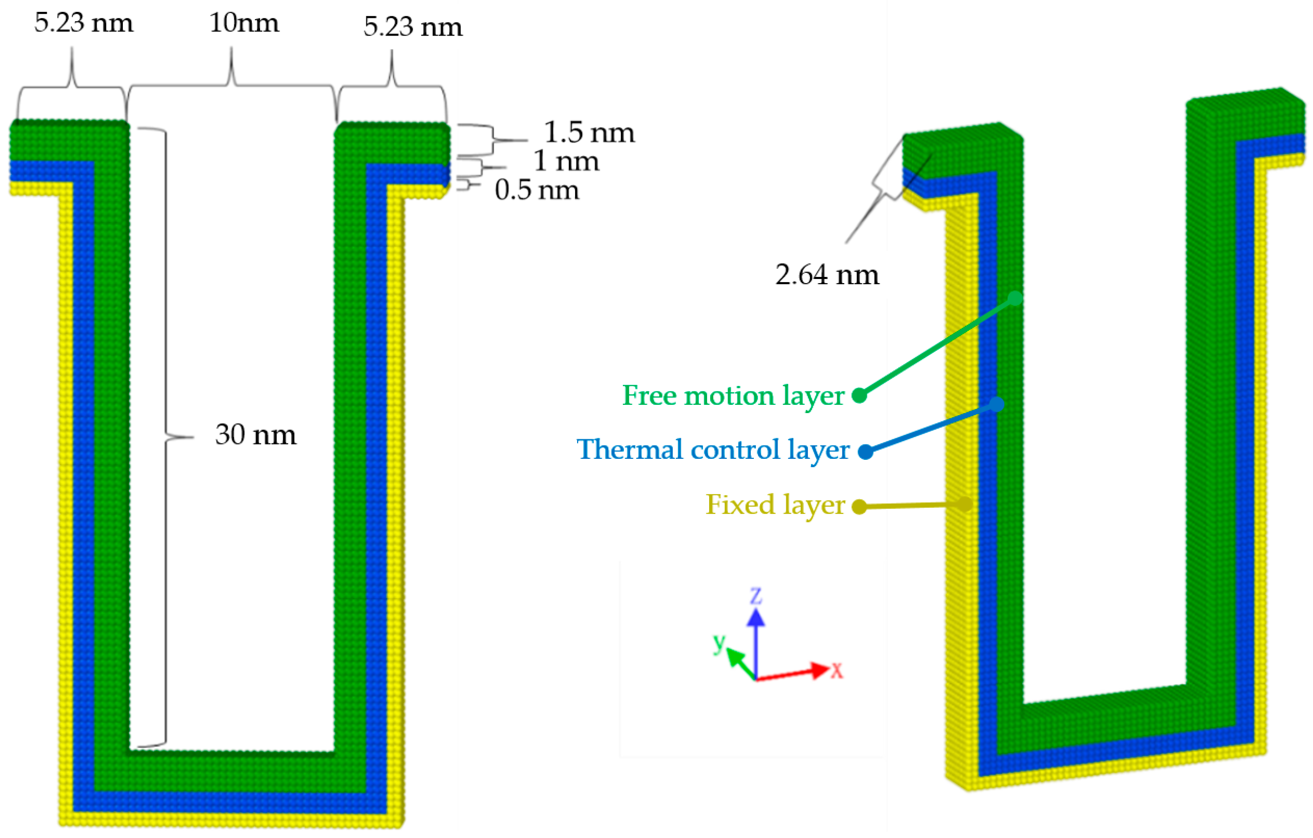
The substrate was composed of three layers: the free motion layer, the thermal control layer, and the fixed layer, as shown in Figure 2. The width of the substrate trench was about 10 nm, the wing (pitch) of the substrate was 5 nm, the height was 30 nm, and the depth was 2.5 nm, with a slight difference between different materials. The free motion layer was marked as green. Atoms in the free motion layer could interact with thermal control layer atoms and the incident atoms freely for copper deposition. The thermal control layer was marked as blue. The temperature of the atoms in thermal control layer was modified by the Langevin thermostat [20] as follows:
P ˙ i = m i v ˙ i = U m i γ i v i + 2 γ k B T R ( t )
where P i is the momentum of atom i ; m i is the mass of the atom i ; v i is the velocity of the atom i ; U is the particle interaction potential; is the gradient operator such that U is the force calculated from interatomic potentials; γ is the viscosity; T is the temperature; kB is Boltzmann’s constant; and R(t) is delta-correlated stationary Gaussian distributed random force. The fixed layer was marked as yellow. Forces acting on the atoms in the fixed layer were set as 0 to prevent the substrate from moving, which presented the stability of the substrate in reality.
The temperatures of the substrate discussed in this study were 350 K, 500 K, 650 K, 800 K, and 950 K, respectively, since the typical process temperature for physical vapor deposition is between 520 K and 720 K, and in some cases, ionized physical vapor deposition can be deposited at temperatures below 340 K or up to 870 K, depending on the expected behavior in the application.
The materials of the substrate are discussed in the literature review section, which are Ta/TaN, Ti/TiN, Ti/TiN/Ti, Co/TaN, Mo/MoN, and W/WN. Since the cut-off radius is about 5 Å to 10 Å, only the liner of the substrate is considered. Thus, the material of the substrate is the liner material, which in this study were tantalum (Ta), titanium (Ti), molybdenum (Mo), cobalt (Co), and tungsten (W). The crystal structure and lattice parameters of each material are shown in Table 1. The orientation of the substrate was (1 0 0) for bcc and (0 0 0 1) for hcp. For tantalum, crystal planes of (1 0 0), (1 1 0), (1 1 1) were discussed in this study.

2.5. Deposition Model

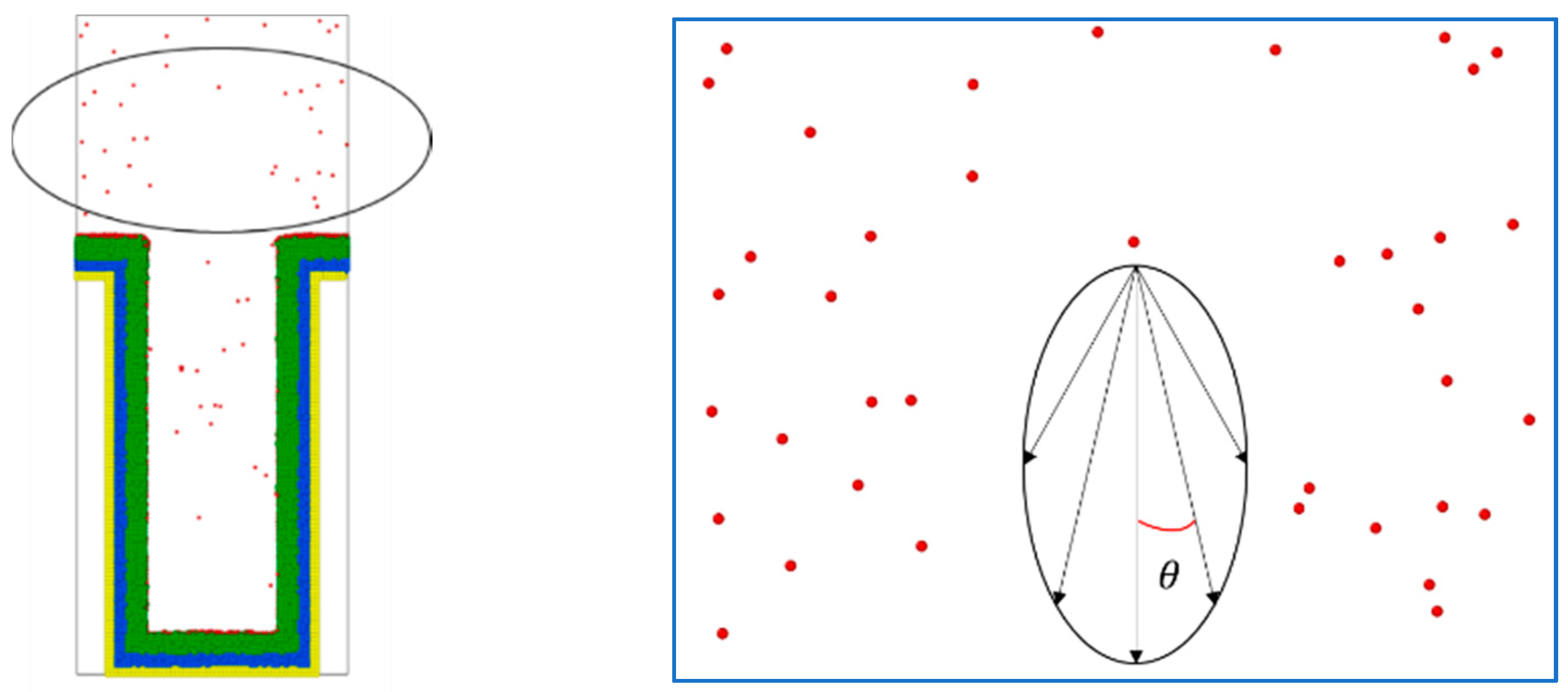
Copper atoms were marked as red and were released from 5000 Å above the substrate trench with uniform and random distributions in the x and y directions, as shown in Figure 3. A total of 18,000 copper atoms was deposited, and the results were calculated after the system reached steady state.
The velocity of incident atoms is dependent on the incident energy. The incident energy values of the copper discussed in this study were 1 ev, 3 ev, 5 ev, 7 ev, and 10 ev, respectively. The deposition of PVD copper in this study was set as cosine distribution, as illustrated in Figure 3. As the angle of cosine distribution was restricted, the deposition could be approximated to IPVD. The deposition zenith angle discussed in this study was −5 ° to 5 ° , −10 ° to 10 ° , −30 ° to 30 ° , −50 ° to 50 ° , and −70 ° to 70 ° , respectively, while the range of azimuth angle was from 0 ° to 360 ° .
A typical deposition rate of sputtering is about 10–50 nm/min. However, due to the limitation of molecular dynamics, the deposition rate in this study was set as 50 atoms/ps, 30 atoms/ps, 10 atoms/ps, 7 atoms/ps, 5 atoms/ps, 3 atoms/ps, and 1 atom/ps, which is larger than the actual process. The results of the copper seed layer with respect to the deposition rate are discussed in the following section.

3. Results and Discussion

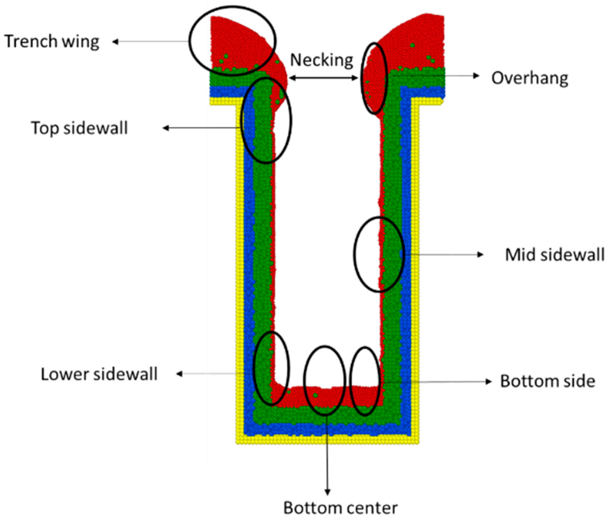
According to the trench model shown in Figure 4, the parameters applied to study the results of the deposited copper seed layer are defined as follows:
  • Step coverage is defined as the average number of atoms deposited on the target region over the average number of atoms deposited on wing of the trench.
  • Uniformity is defined as the average number of atoms deposited on the top sidewall over the average number of atoms of the overhang.
  • Bottom height is defined as the average height of atoms accumulated at the bottom of the trench.
  • Alloy percentage is defined as the percentage of substrate atoms in the copper seed layer.
  • Necking is defined as the distance between the atoms at the two trench necks.
The influences of substrate temperature, incident energy, incident angle, crystal plane, and liner materials on the sputtering process are illustrated and discussed below.

3.1. Substrate Temperature

The dominant factor of different substrate temperatures is the thermal energy of the substrate atoms. Substrate temperatures of 350 K, 500 K, 650 K, 800 K, and 950 K were discussed in this study. To investigate the effect of substrate temperature, tantalum was selected as the substrate material, while the other parameters were set as follows: incident energy = 5 ev, deposition height = 5000 Å, incident angle = 30°, and deposition rate = 10 atoms/ps. The corresponding copper seed layers under different substrate temperature at 2500 ps are shown in Figure 5.
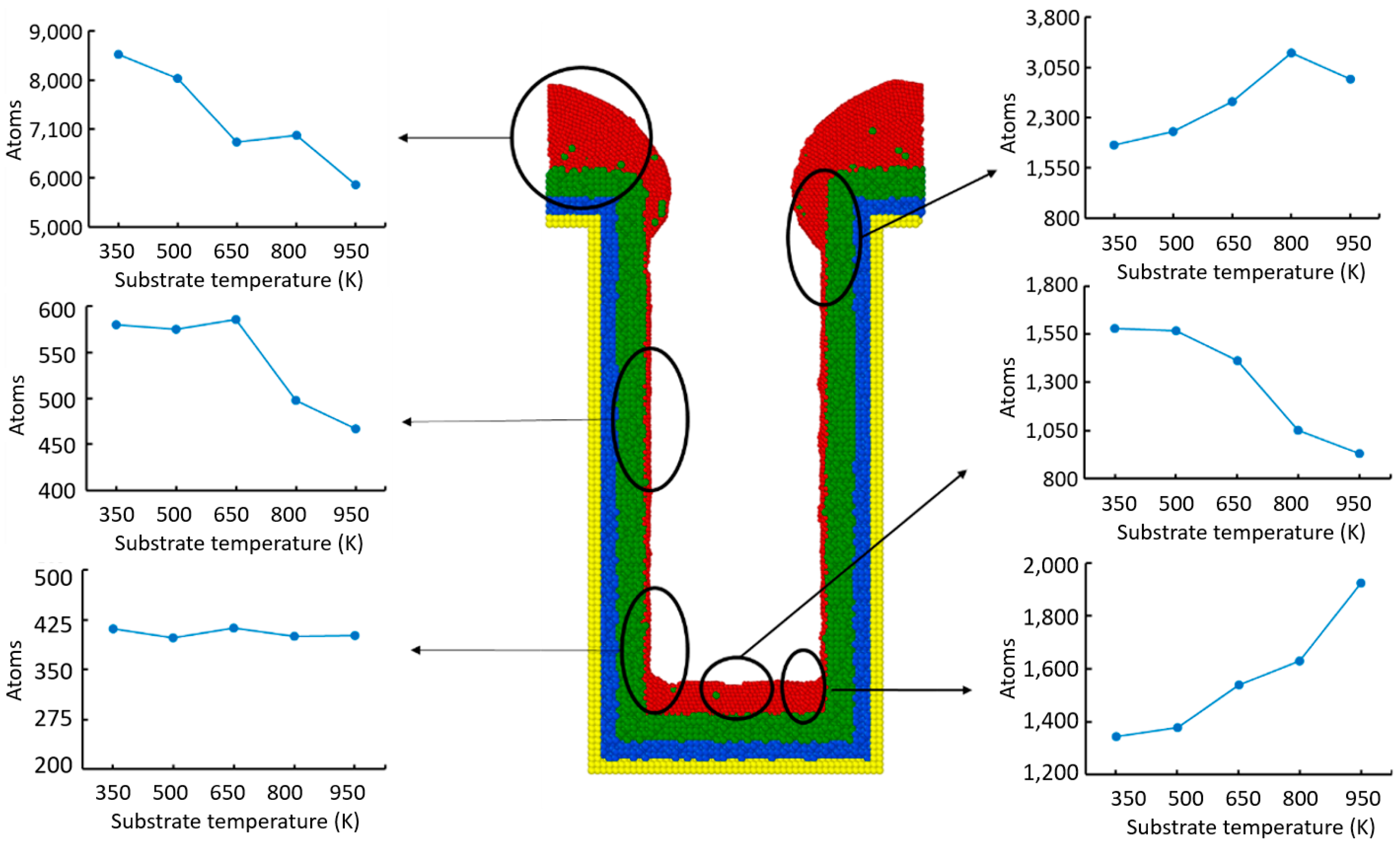
By increasing the temperature of the substrate, thermal energy of the substrate atoms increased, which also delivered the thermal energy to the deposited copper. Consequently, this increased the diffusivity of both the substrate atoms and the deposited copper atoms. Overall distribution of the deposited copper atoms with respect to substrate temperatures is shown in Figure 6.
At the wing of the trench, copper atoms gradually diffused into the trench and accumulated at the top sidewall, which caused the necking to decrease. As necking decreased, the number of atoms reaching mid sidewall would also decrease. The situation at the lower sidewall was more complicated; with the decreasing necking, atoms reaching the lower sidewall decreased. However, with the increasing diffusivity caused by the increasing temperature, atoms from the island at the bottom diffused to the lower sidewall. No significant change of number of atoms at the lower sidewall was observed due to the equalizing influence of necking and diffusivity.
To the bottom of the trench, the increasing temperature gave the atoms on the center island more energy to break through the diffusion barrier energy and diffuse to the two sides of the trench, which led to a decrease in number of atoms at the bottom center of the trench and an increase at the two sides of the trench.
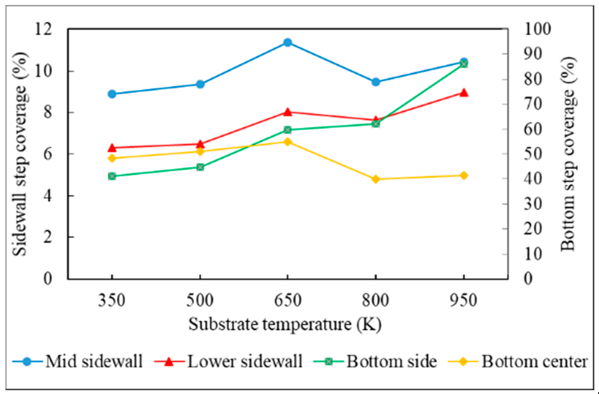
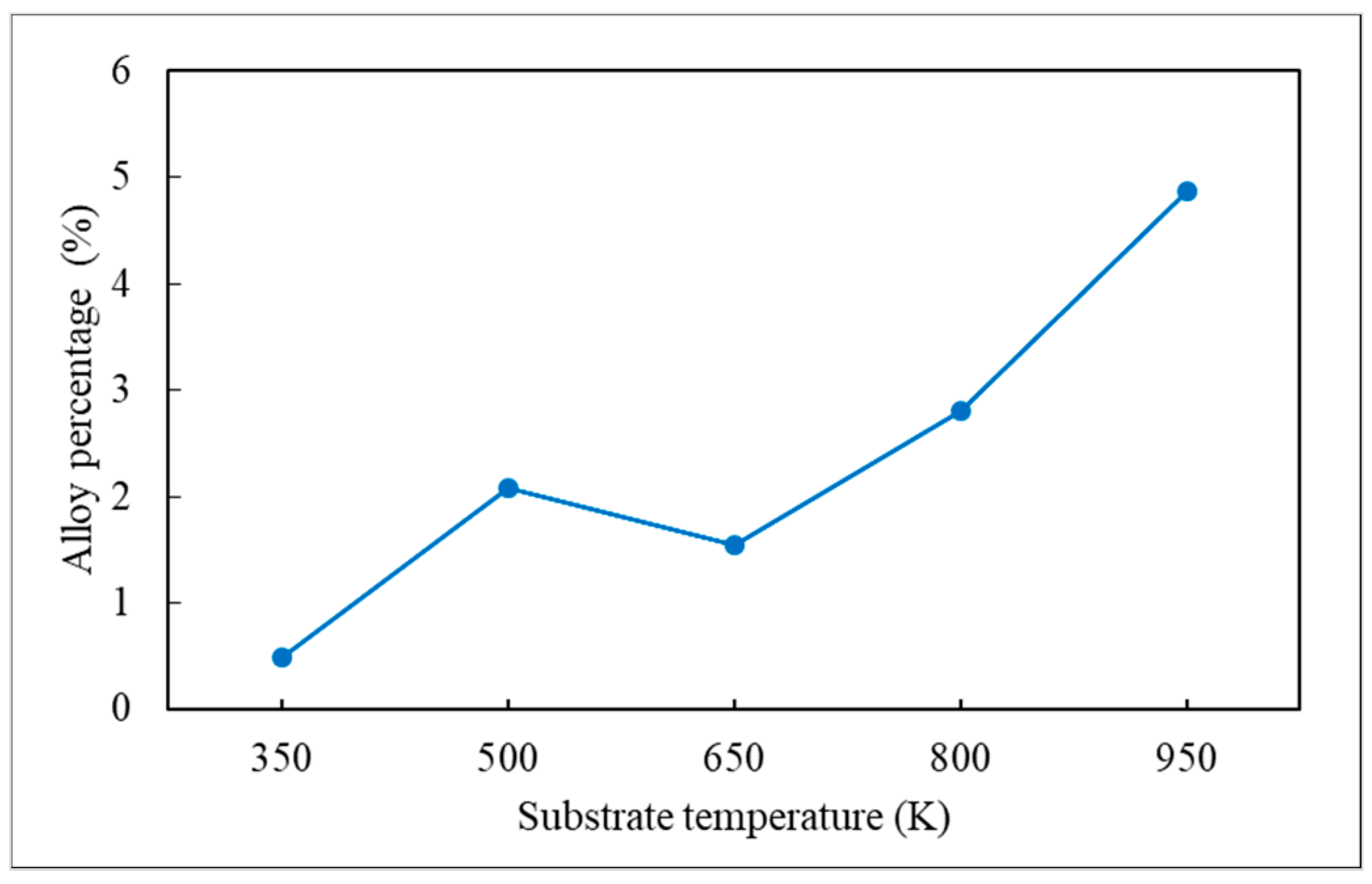
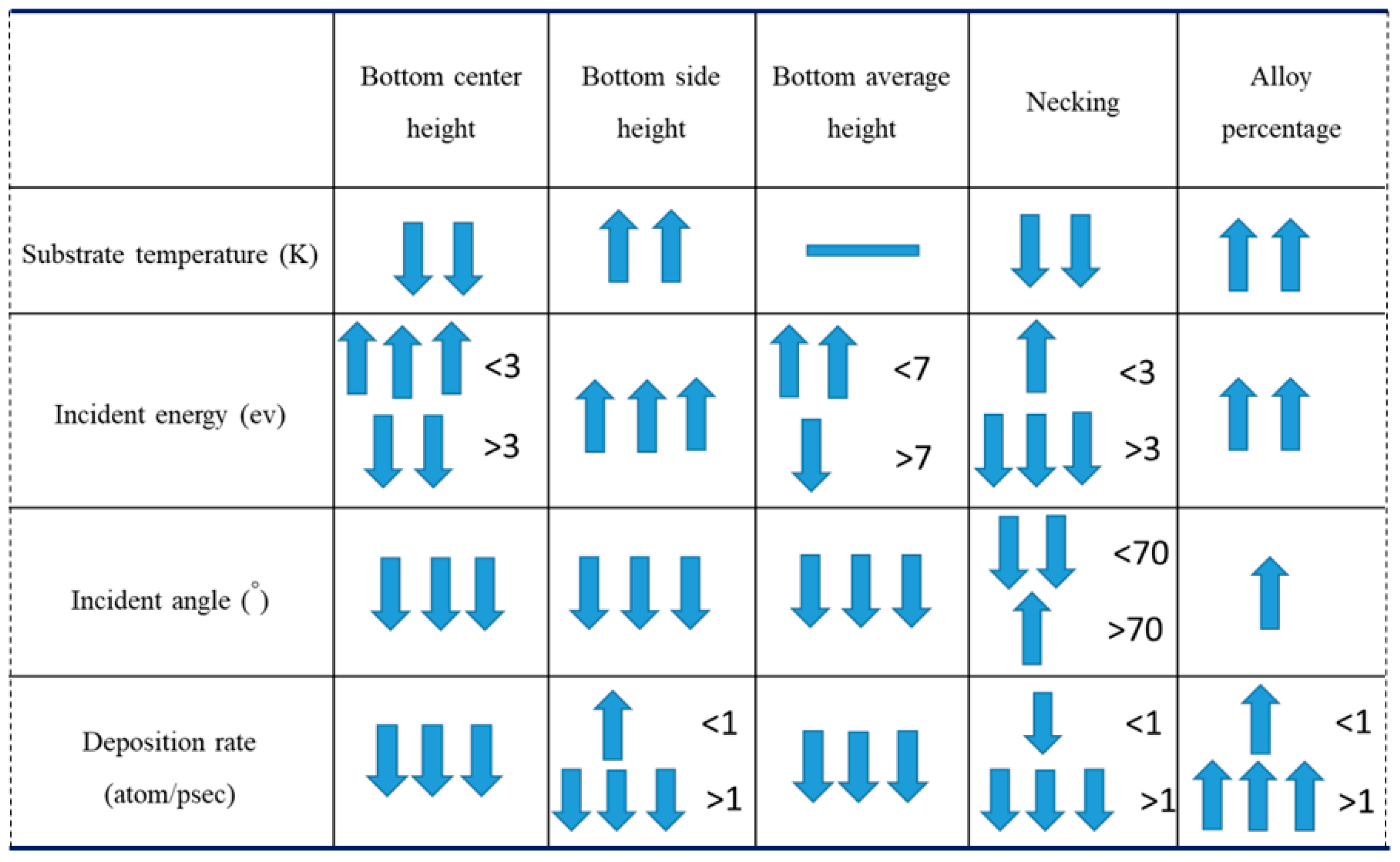
As for the substrate atoms, the increase in thermal energy caused them to flow into the deposited copper, which resulted in impurity of the copper seed layer. These mechanisms led to the results of step coverage, uniformity, necking, bottom height, and alloy percentage, as shown in Figure 7, Figure 8, Figure 9 and Figure 10, under different substrate temperatures. Unlike the others, the step coverage of the bottom center decreased significantly for substrate temperatures higher than 650 K, as shown in Figure 7. On average, the uniformity decreased when substrate temperatures increased, as illustrated in Figure 8. Figure 9 shows that the change of height of the copper seed layers of different regions did not have consistency as temperature increased. The neck of the copper seed layer became narrower when substrate temperatures increased. Figure 10 reveals that the alloy percentage of the copper seed layer increased as more and more substrate atoms flowed into the copper seed layer due to an increase of substrate temperature.

3.2. Incident Energy

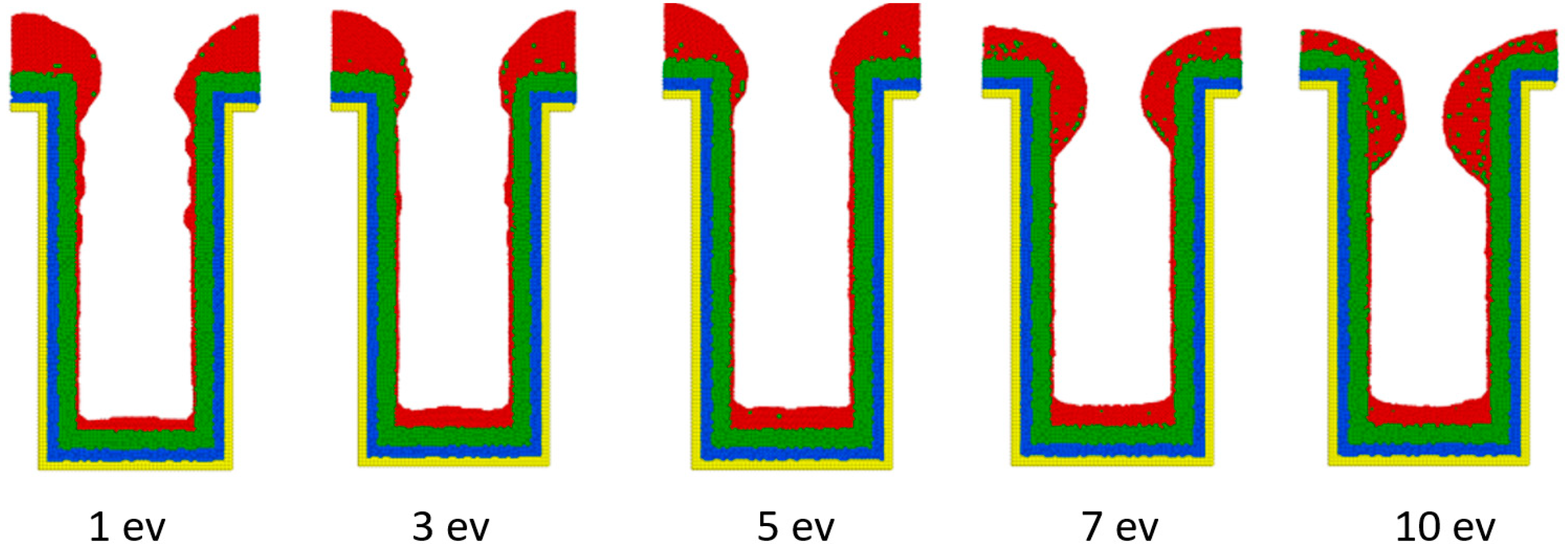
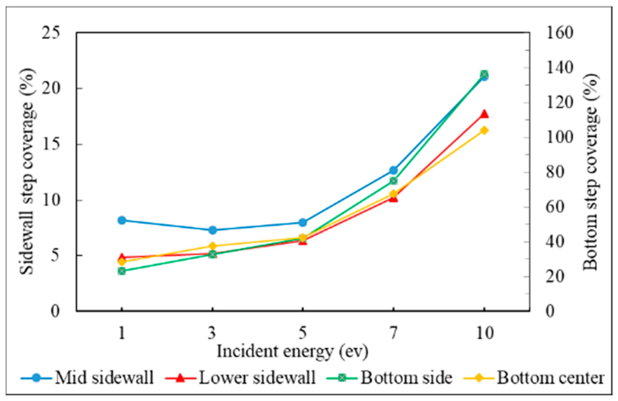
Incident energy of the sputtered copper atoms depends on the power of RF generator, which generates plasma and ionized argon to sputter the copper target. Incident energy values of 1 ev, 3 ev, 5 ev, 7 ev, and 10 ev were discussed in this study. To study the effect of incident energy, tantalum was selected as the substrate material, while the other parameters were set as follows: deposition height = 5000 Å, incident angle = 30°, substrate temperature = 600 K, and deposition rate = 10 atoms/ps. The resulting copper seed layers with different incident energies are shown in Figure 11.
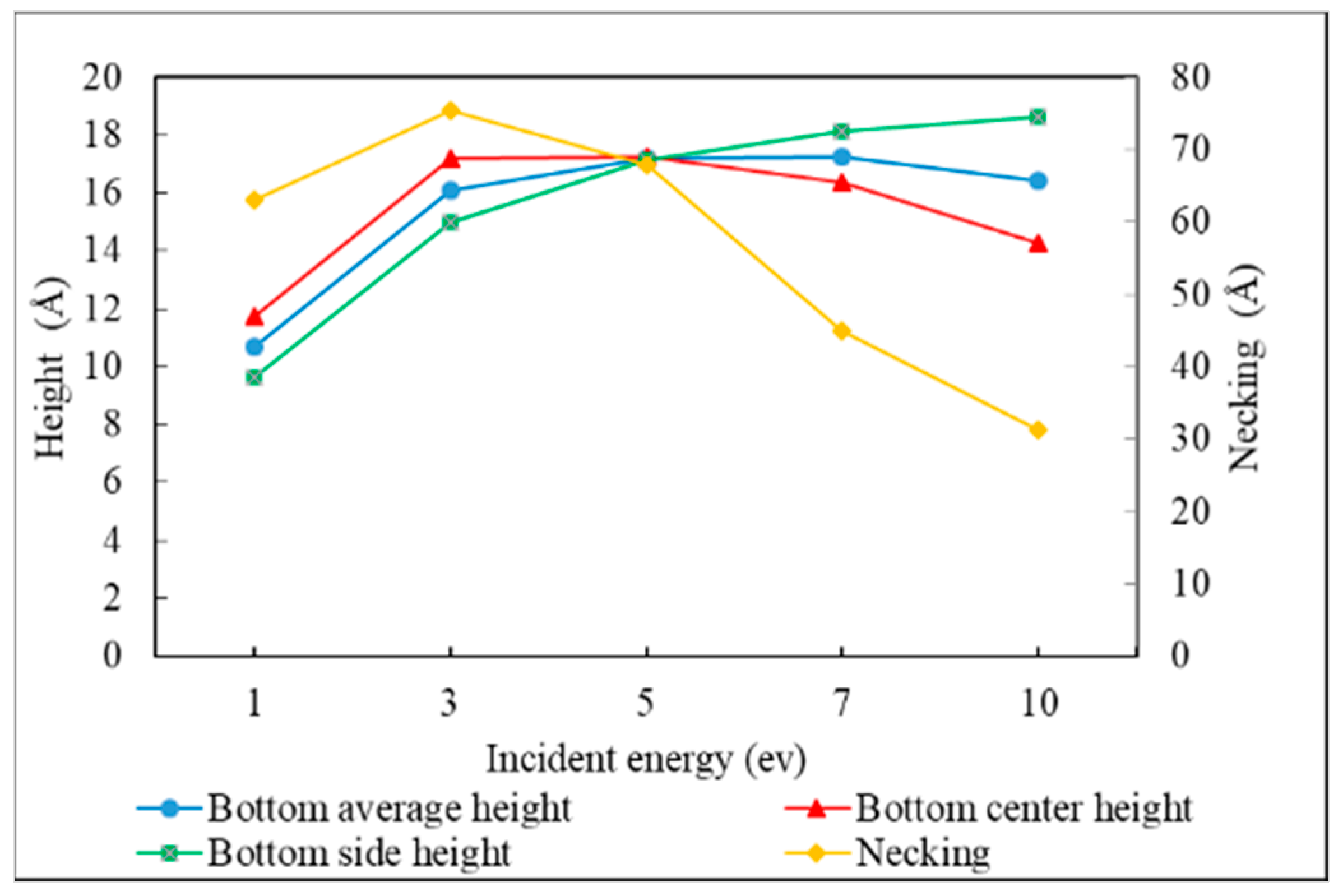
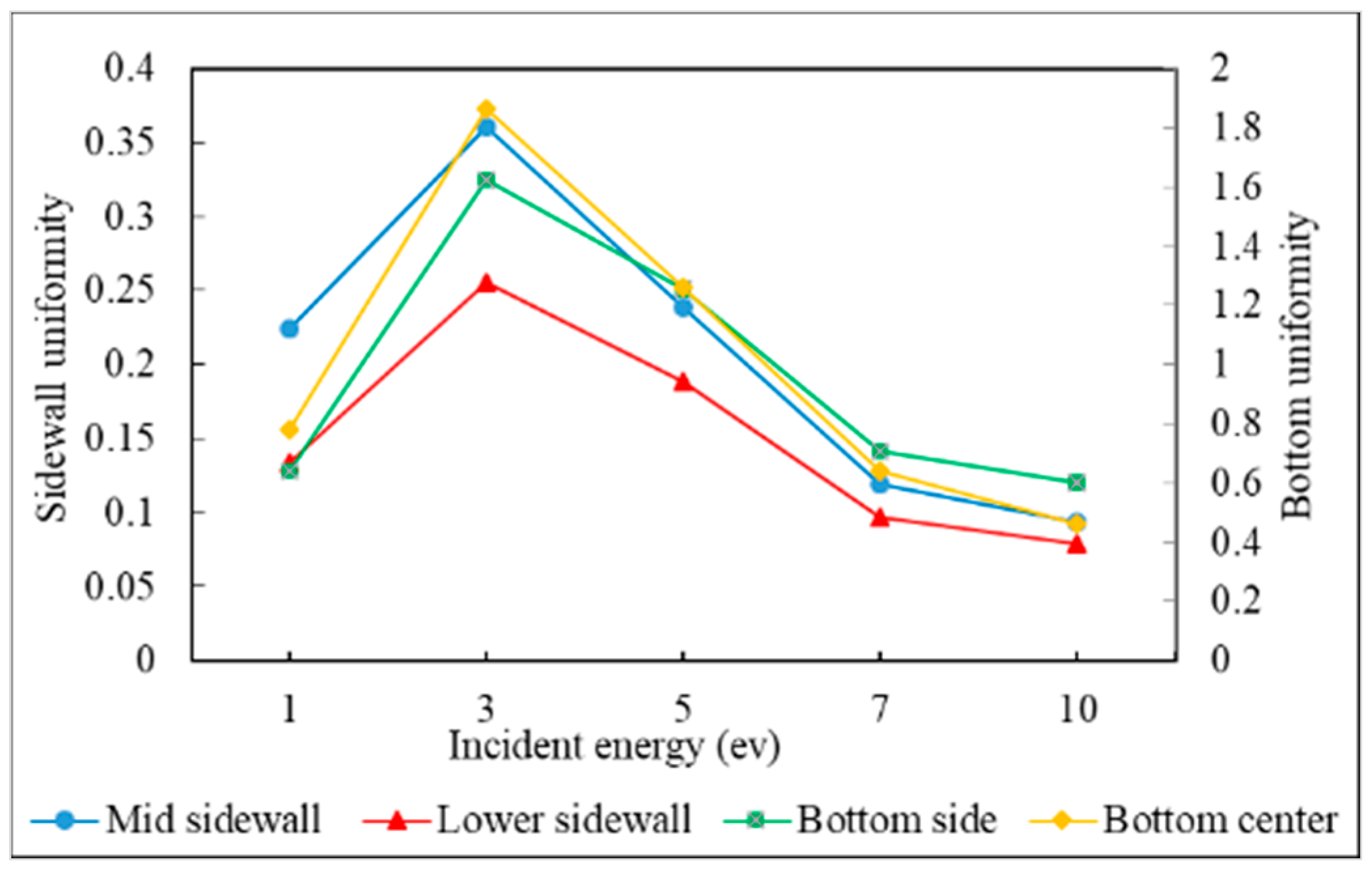
Copper atoms with higher incident energy transferred more kinetic energy to the deposited atoms and substrate. This gave atoms more energy to break through the diffusion barrier energy. The overall distribution of the deposited copper atoms with respect to incident energy is shown in Figure 12. The additional energy given by the depositing atoms led the deposited atoms to flow into the trench and accumulate at the top sidewall, which caused the necking to decrease. The smaller the necking, the fewer atoms reaching the mid sidewall. Around the lower sidewall, with decreasing necking, atoms reaching the lower sidewall decreased. However, with increasing diffusion ability caused by the increasing energy, atoms from the island at the bottom diffused to the lower sidewall. Figure 13 shows that the necking of the copper seed layer decreased as the incident energy increased. The step coverage of all regions increased as the incident energy increased, as shown in Figure 14. The effect of diffusivity dominated when the incident energy was smaller than 5 ev. As energy exceeded 5 ev, the shadowing effect became dominant. It is noted that in the case of 1 ev, since the incident energy was low, atoms were more likely to be captured at the top sidewall rather than depositing further into the trench; consequently, this resulted in poor uniformity, as shown in Figure 15.
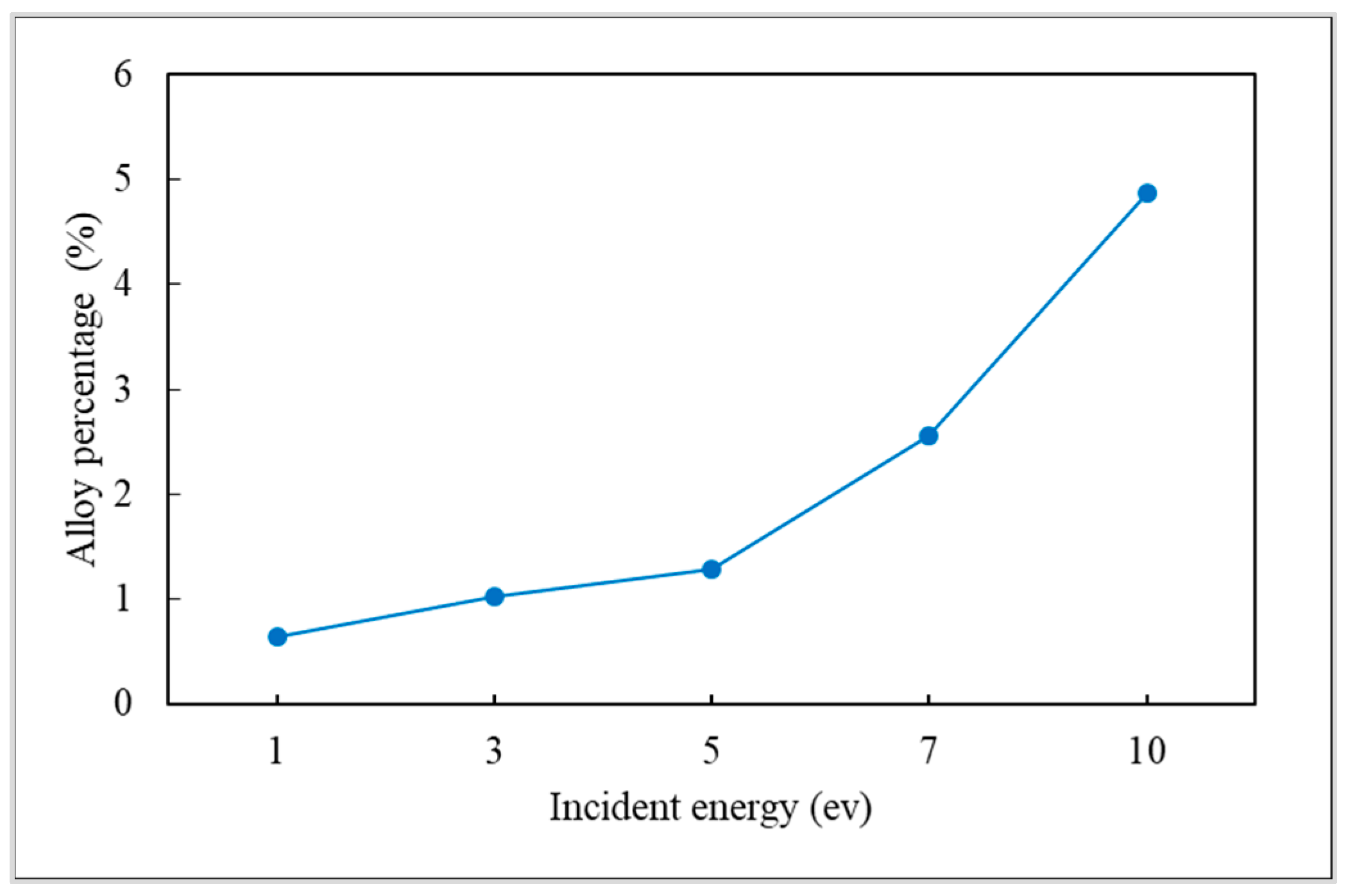
To the bottom of the trench, the increasing incident energy gave the atoms on the center island more energy to break through the diffusion barrier energy and diffuse to the two sides of the trench. This led to a decrease in number of atoms at the bottom center of the trench and an increase at the bottom sides of the trench. For the substrate atoms, the increase in incident kinetic energy caused them to flow into the copper seed layer, which increased the alloy percentage, as shown in Figure 16.

3.3. Incident Angle

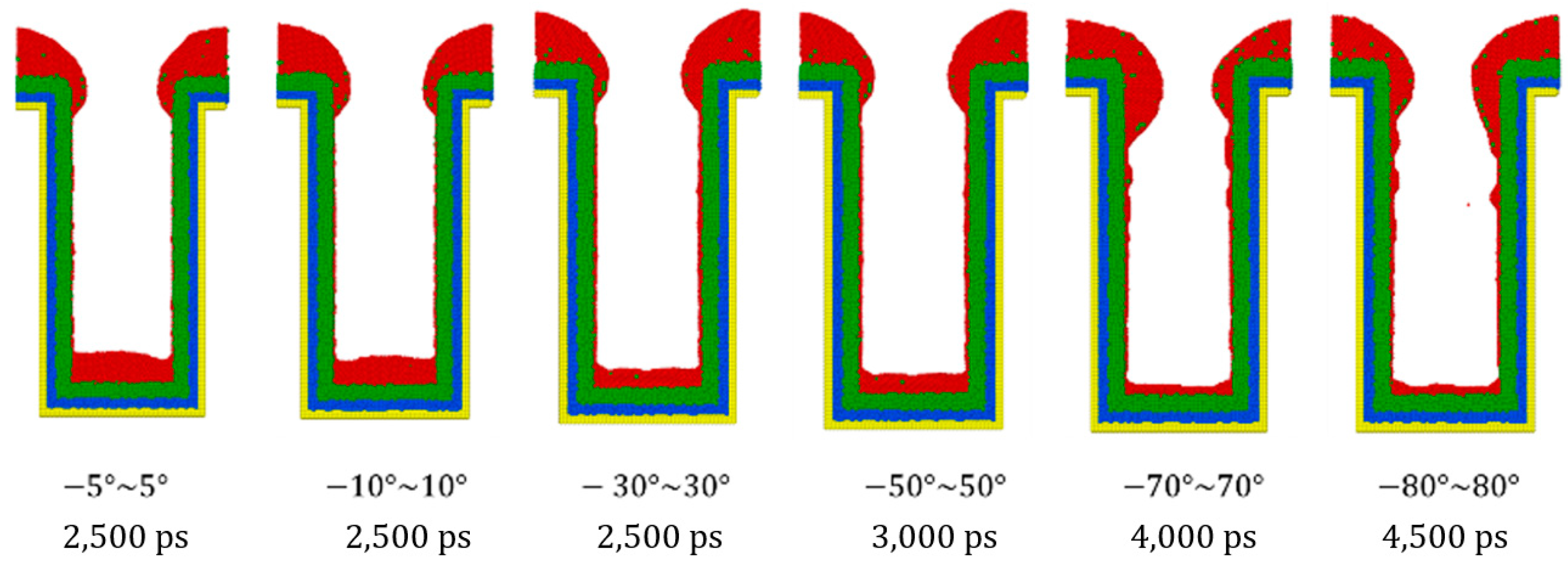
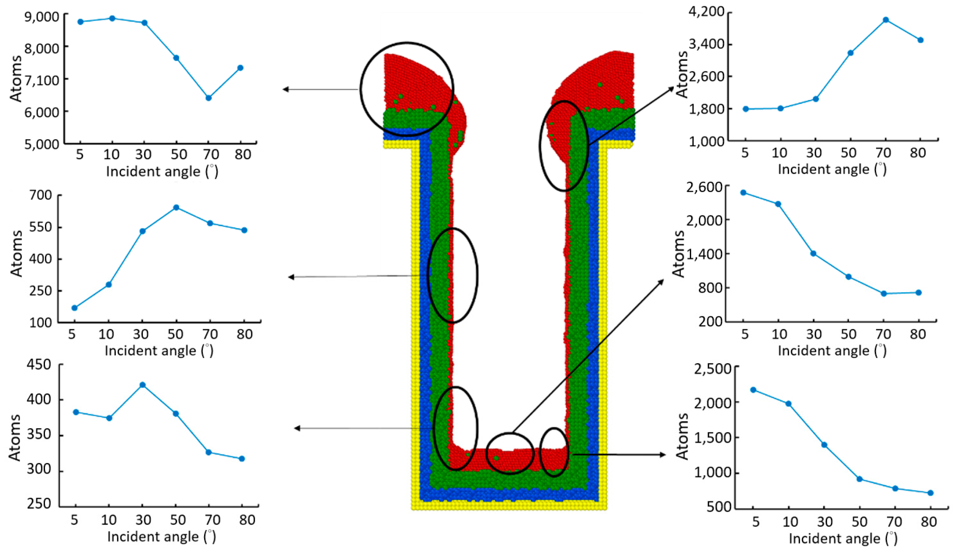
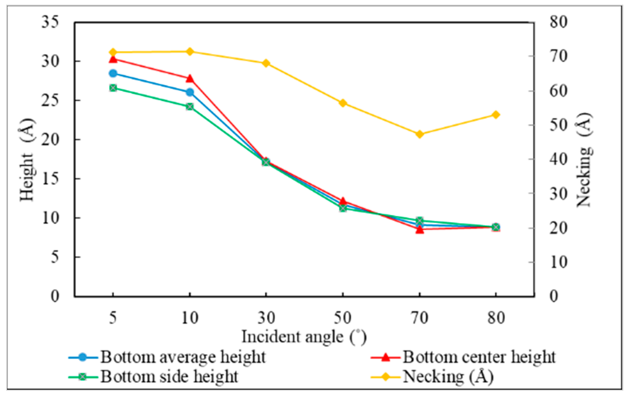
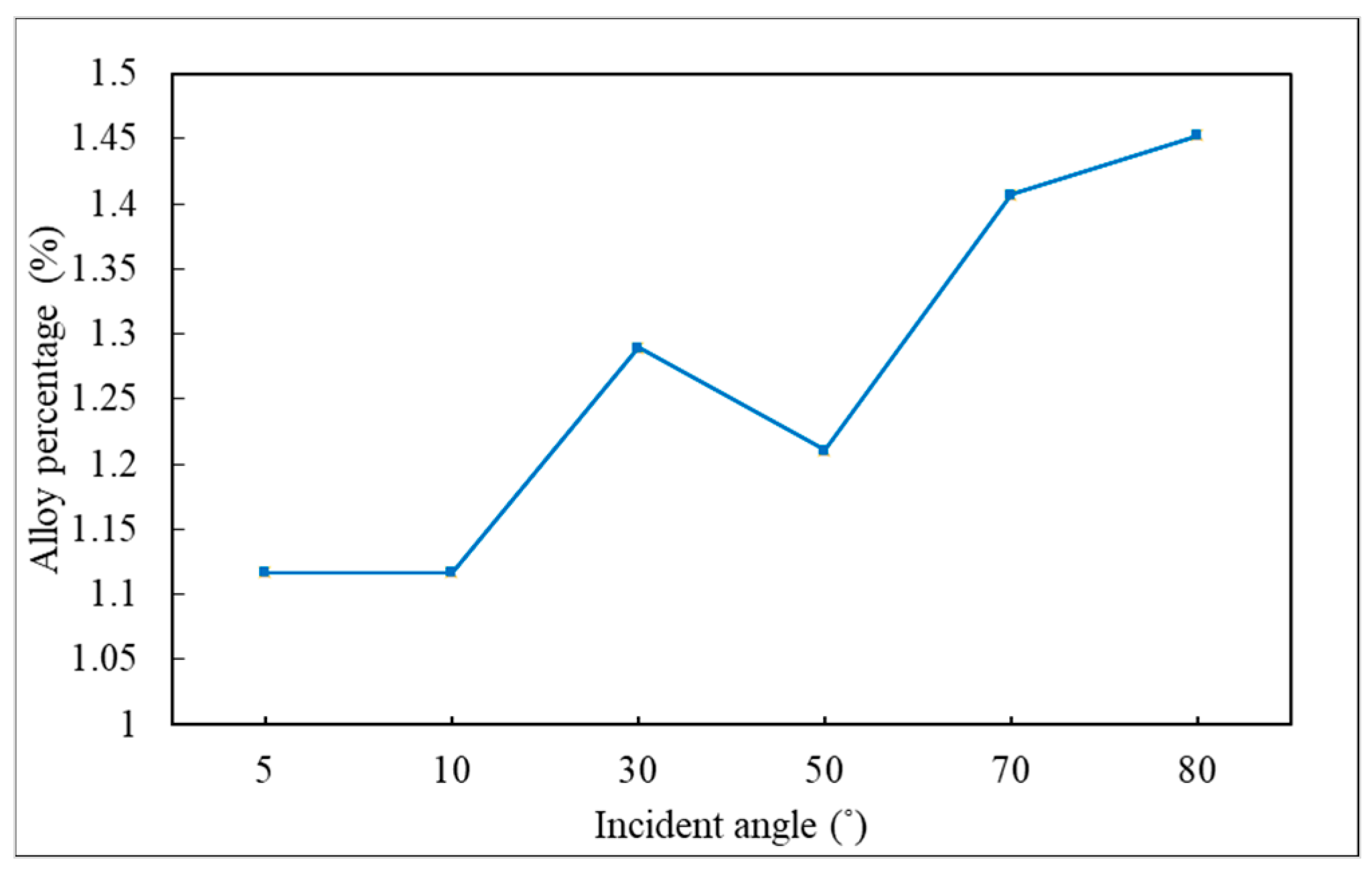
The incident angle of copper atoms determines the arrival angle and the possible area of the trench on which these atoms deposit. By increasing the incident angle, it is more likely that the copper atoms can reach the sidewalls. Incident angle of the copper atoms can be controlled by bias during the deposition process. Incident angles of 5°, 10°, 30°, 50°, 70°, and 80° were discussed in this study. To study the effect of incident energy, tantalum was selected as the substrate material, while the other parameters were set as follows: incident energy = 5 ev, deposition height = 5000 Å, substrate temperature = 600 K, and deposition rate = 10 atoms/ps. The resulting copper seed layers under different incident angles are shown in Figure 17, and the overall distributions of the deposited copper atoms with respect to incident angles are illustrated in Figure 18. With more and more atoms arriving at the sidewall, the number of atoms deposited at the top sidewall increased significantly. This decreased the necking of the copper seed layer.
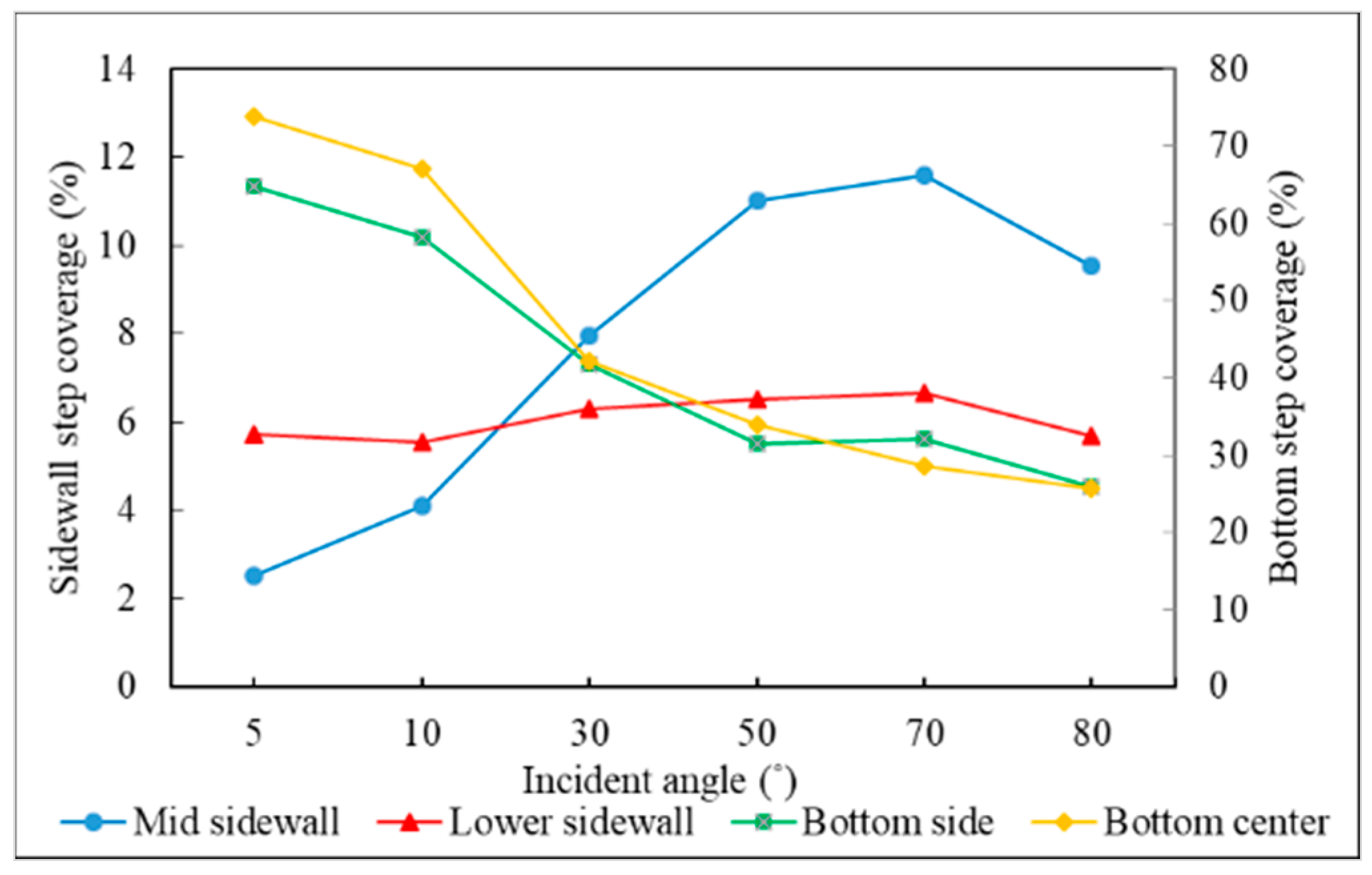
At the mid and lower sidewalls, more and more atoms reached the sidewall by increasing the incident angle, However, this was not always the case for the mid sidewall and lower sidewall. As the incident angle exceeded 30°, atoms were more likely to deposit at the top sidewall and mid sidewall rather than the lower sidewall, while as incident angle exceeded 50°, atoms were more likely to deposit at the top sidewall rather than the mid sidewall. Thus, the deposited atoms at lower sidewall started to decrease after the incident angle of 30°, while the deposited atoms at the mid sidewall started to decrease after the incident angle of 50°. As for the bottom center and bottom side, atoms were less likely to reach the bottom of the trench with increases of the incident angle.
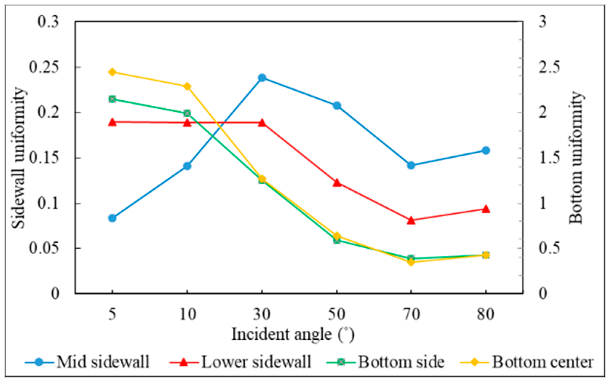
As shown in Figure 19, the step coverage of the mid sidewall increased in general with an increase of incident angle, while the bottom center and bottom side step coverage decreased. Figure 20 reveals that the uniformity of the mid sidewall increased for incident angles of 5° to 30° but decreased as angles exceeded 30°. The uniformity of the lower sidewall decreased after 30°. The bottom center and bottom side uniformity decreased as the incident angle increased. Figure 21 shows that the average bottom height of the copper seed layer decreased, and the necking of the copper seed layer decreased with an increase of incident angle. The alloy percentage of the copper seed layer increased slightly as the incident angle increased, as illustrated in Figure 22.

3.4. Deposition Rate

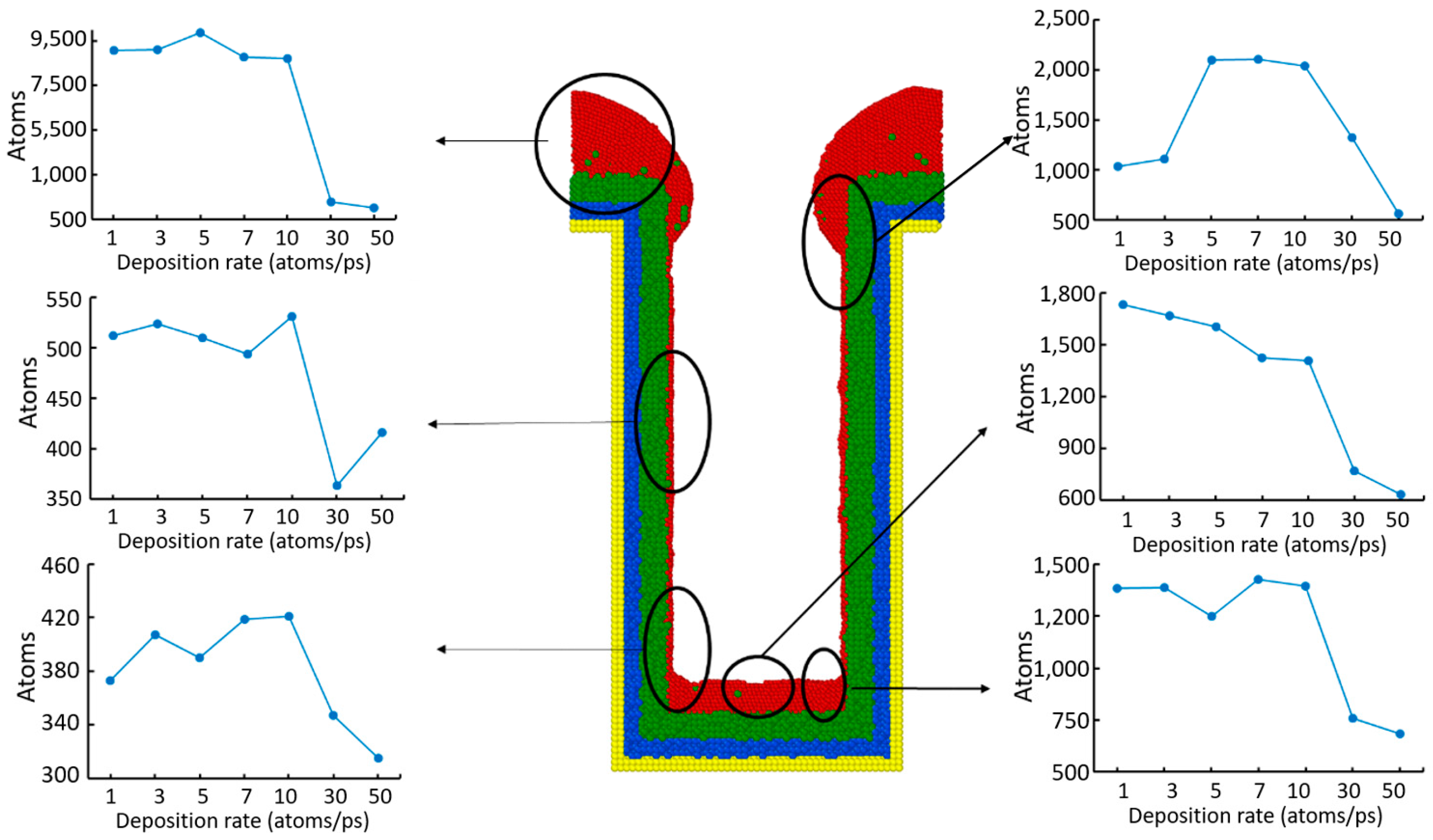
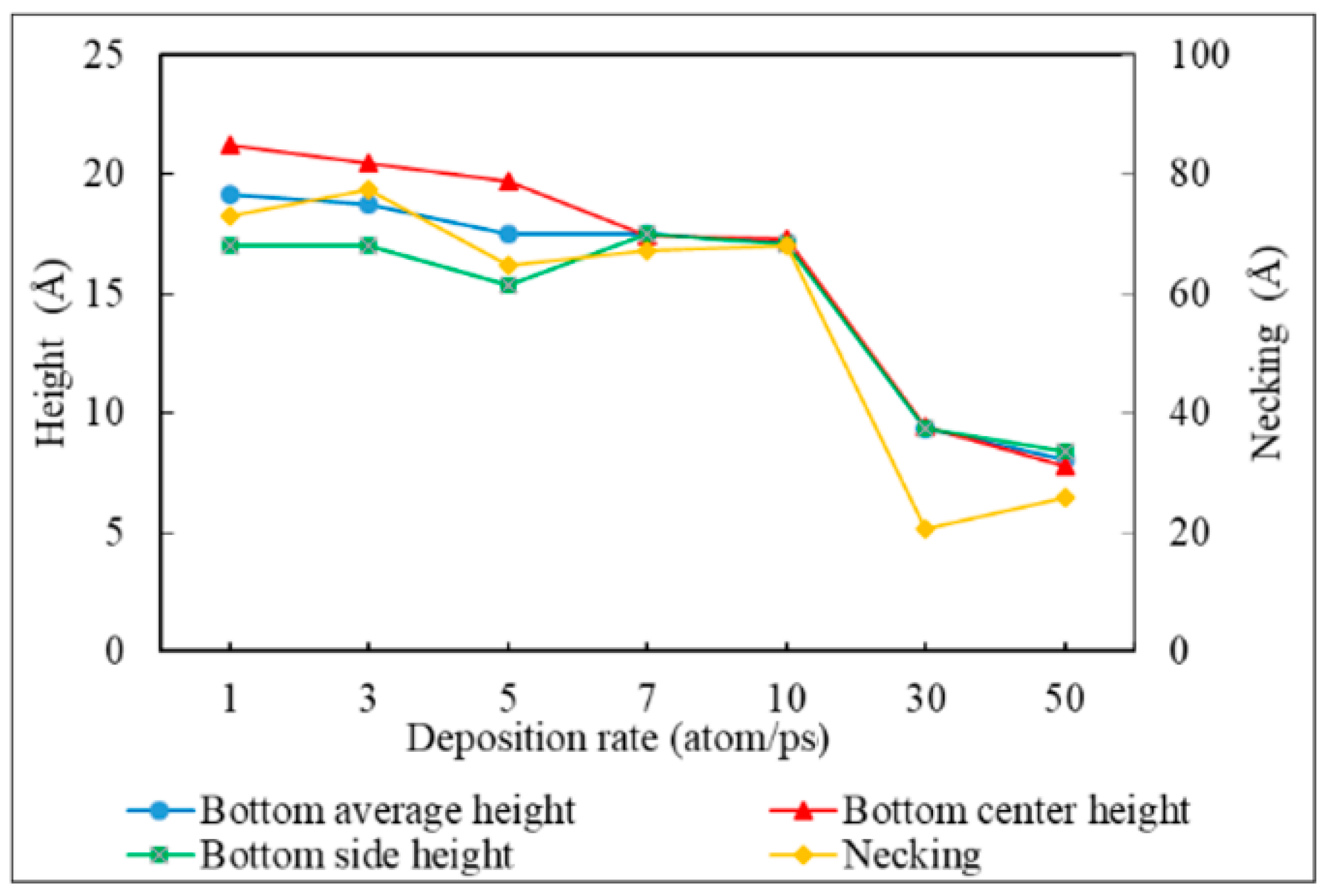
The dominant factor of different deposition rates is the collision of depositing and deposited atoms, and the effect of Ostwald ripening. With a higher deposition rate, the energy transferred by the depositing atoms to the deposited atoms increases, giving the copper atoms more energy to flow to the low deposited area, while with a lower deposition rate, more surface diffusion of Ostwald ripening occurs due to longer deposition time. The copper seed layer with different deposition rates is shown in Figure 23 and Figure 24 and illustrates the overall distribution of the deposited copper atoms with respect to deposition rates.
The energy transferred between atoms occurred at a high deposition rate, i.e., at the rate of 50 atoms/ps and 30 atoms/ps in this study, while surface diffusion dominated at a low deposition rate under 10 atoms/ps. Under the circumstances of high deposition rate, by increasing the deposition rate, the energy transferred from the depositing atoms to the deposited atoms at the wing of the trench made them flow into the trench and accumulate at the top sidewall. The cluster atoms at the top sidewall also flowed into the trench, which caused the necking to increase.
To the mid sidewall and lower sidewall, the number of atoms increased significantly at the mid sidewall as atoms from the top sidewall flowed into the trench. The number of atoms at the lower sidewall, however, decreased, as many copper atoms accumulated in a huge cluster rather than depositing to the area below the mid sidewall. As for the bottom of the trench, the large cluster at the sidewall received most of the depositing atoms towards the bottom of the trench, thus decreasing the number of atoms at the bottom of the trench. It is also noted that since the deposition rate of 50 atoms/ps received more energy from the depositing atoms, atoms at the bottom center flowed toward the two sides, and the atoms at the two sides flowed to the lower sidewall. This increased the number of atoms at the lower sidewall and the bottom side and decreased the number of atoms at the bottom center.
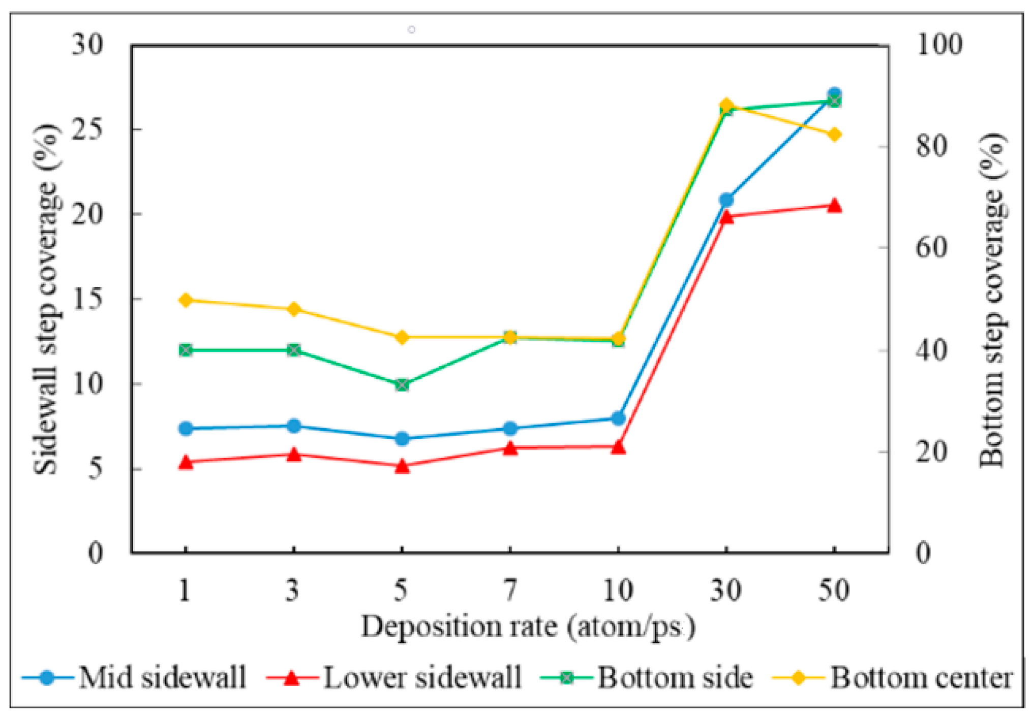
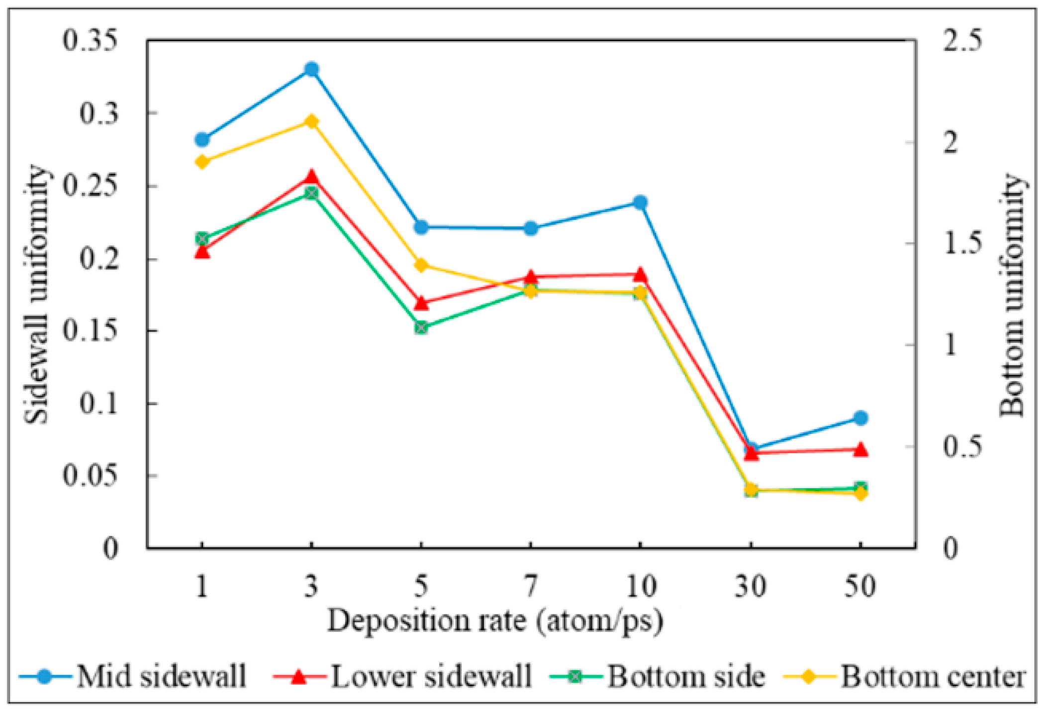
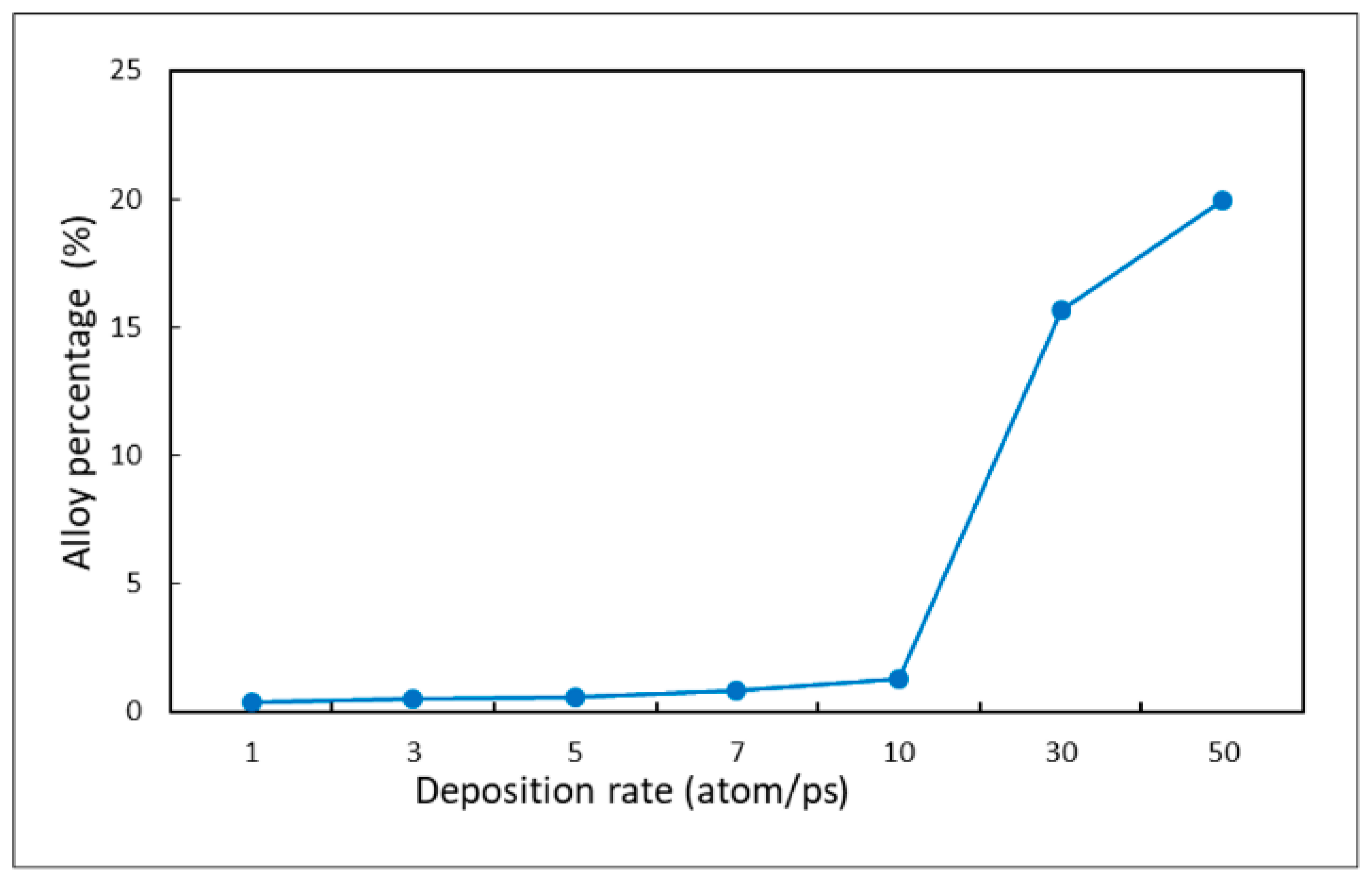
Under the circumstances of low deposition rate, by decreasing the deposition rate, there was no additional energy given by the depositing atoms for the atoms at the wing to break through the diffusion barrier energy, while Ostwald ripening caused the atoms on the top sidewall to flow towards the wing of the trench. This caused an increase in number of atoms at the wing and a decrease in number of atoms at the top sidewall, which also led to an increase of the necking. At the mid sidewall and lower sidewall, the increase of necking decreased the shadowing effect, which caused the depositing atoms at the mid sidewall and lower sidewall to increase. To the bottom of the trench, with the increasing necking, more atoms arrived at the bottom trench, and thus the number of atoms at the bottom center and bottom side increased. These phenomena led to the results of the step coverage, uniformity, necking, and bottom height shown in Figure 25, Figure 26 and Figure 27. It was also observed that as the deposition rate decreased, energy transferred from the depositing atoms to the substrate decreased, which decreased the alloy percentage significantly, as shown in Figure 28.

3.5. Crystal Plane

The dominant factor of different crystal planes is the diffusion barrier energy. Lower diffusion barrier energy increases the diffusivity of the atoms significantly. Various crystal planes on different trench surfaces were studied in this paper. The defined crystal planes studied in this paper are as follows:
  • (100): (100) at X direction, (010) at Y direction, (001) at Z direction.
  • (110) x: (110) at X direction, ( 1 ¯ 10) at Y direction, (001) at Z direction.
  • (110) z: (001) at X direction, (1 1 ¯ ,0) at Y direction, (110) at Z direction.
  • (111) x: (111) at X direction, ( 2 ¯ 11) at Y direction, (0 1 ¯ 1) at Z direction.
  • (111) z: (0 1 ¯ 1) at X direction, (2 1 ¯ 1 ¯ ) at Y direction, (111) at Z direction.
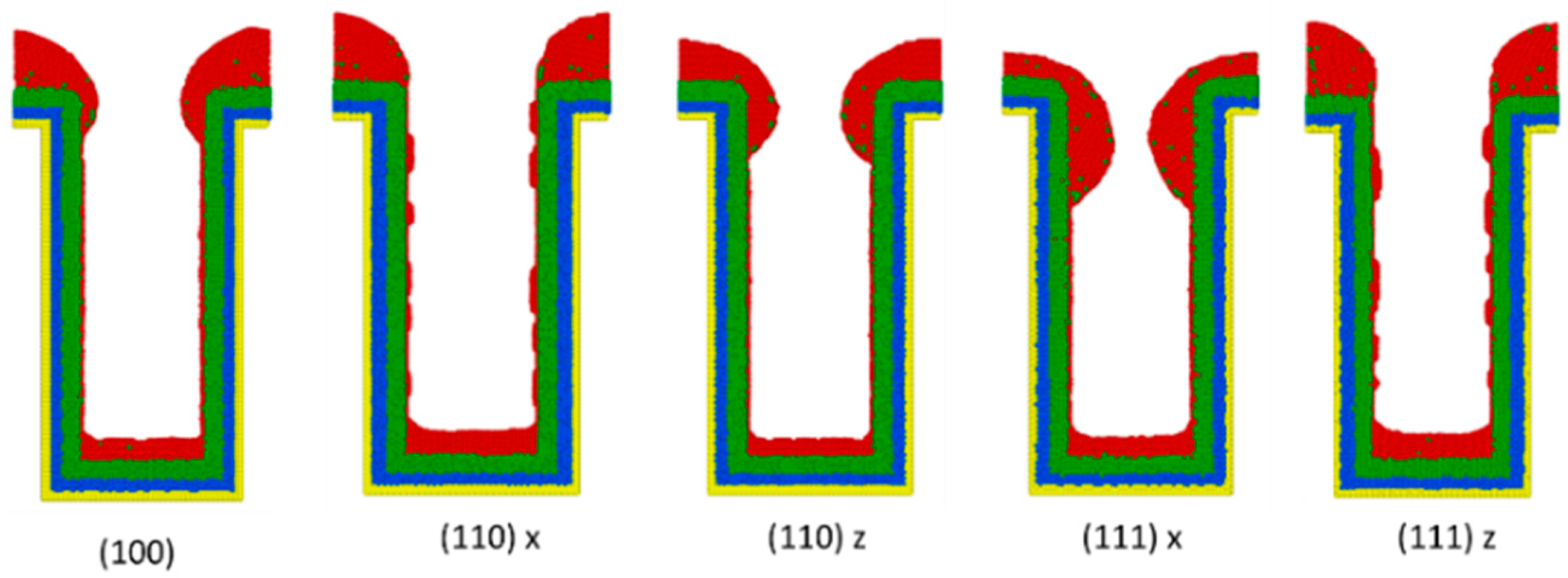
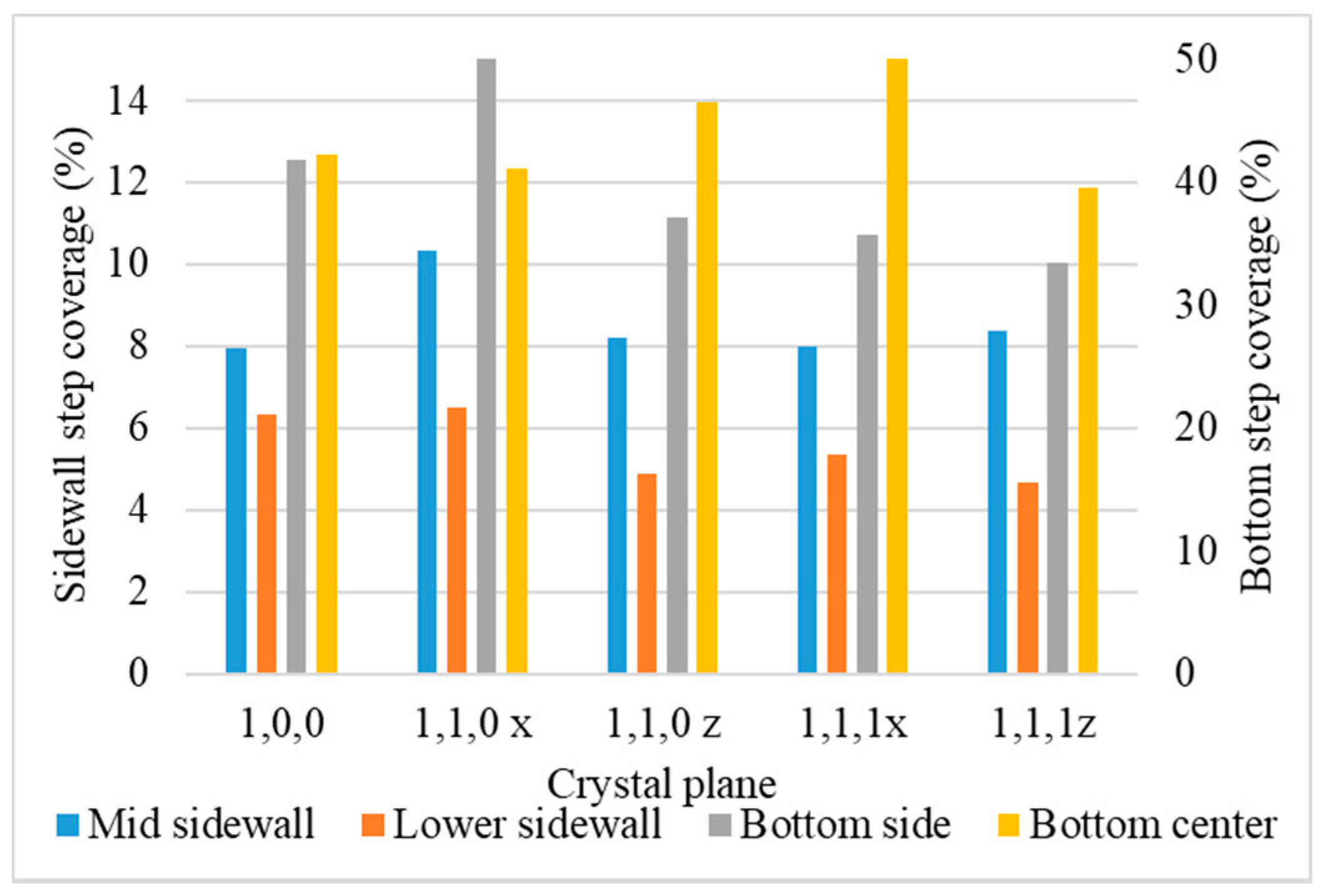
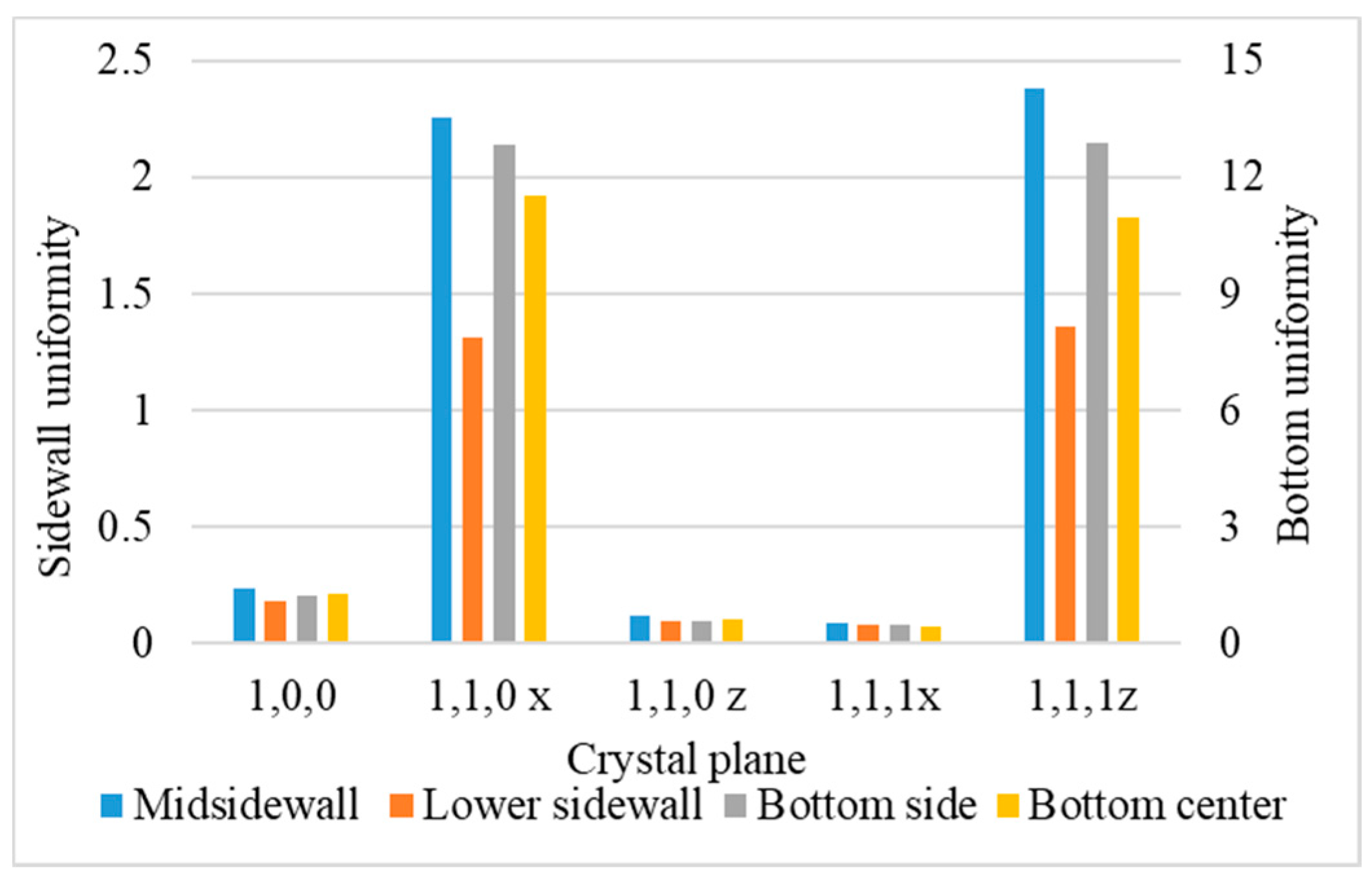
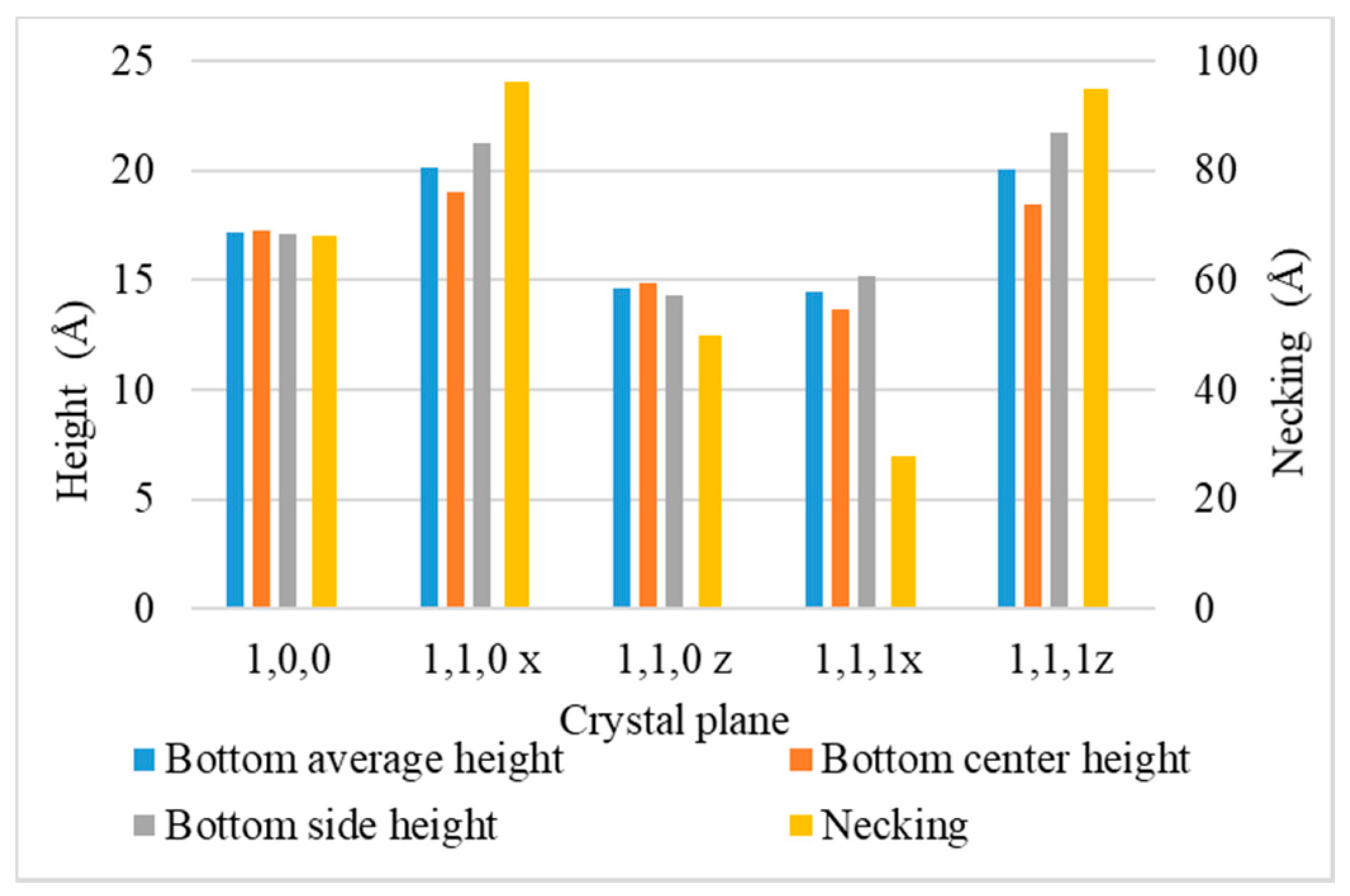
Figure 29 illustrates the copper seed layer with crystal planes. The step coverage and uniformity with different crystal planes are shown in Figure 30 and Figure 31, respectively. Diffusion barrier energy is dependent on the atomic structure of the surface, and it varies between different materials and surface orientations. As shown in Table 2, the diffusion barrier energy of (110) x and (111) z was relatively low in the x direction, while the diffusion barrier energy was high in the z direction, which led to the best uniformity for crystal plane (110) x and (111) z. This caused atoms to diffuse from the top sidewall to the wing more easily than from the wing to the top sidewall. In other words, atoms were more likely to flow from the top sidewall to the wing, rather than the other way around. This decreased the number of atoms accumulating at the top sidewall significantly, and consequently this led to an increase of the necking, as revealed in Figure 32. With the great increase of necking, the number of atoms at sidewalls and the bottom of the trench increased sufficiently. These mechanisms increased the uniformity of the copper seed layer.
The crystal plane of (111) x, however, had high diffusion barrier energy in the x direction and low diffusion barrier energy in the z direction. The low diffusion barrier energy at the wing increased the diffusivity of the atoms, allowing them to flow to the top sidewall, while the high diffusion barrier energy at the sidewall caused most of the atoms to accumulate at the top sidewall, forming huge clusters and decreasing the necking. With the decreased necking, atoms reaching the mid sidewall, lower sidewall, bottom center, and bottom side decreased, causing their uniformity to decrease. This crystal plane, however, led to relatively large step coverage, since the number of atoms at the wing decreased significantly.
It was noticed that crystal planes with larger lattice spacing, such as (111) x and (111) z, allowed the depositing atoms to impact deeper into the substrate, thus increasing the alloy percentage, and vice versa, as shown in Figure 33. In general, this shows that a greater diffusion barrier energy at the wing and lower diffusion barrier energy at the sidewall lead to better uniformity. These mechanisms are caused by the difference of diffusion barrier energy on various crystal surfaces of the trench.

3.6. Liner Materials

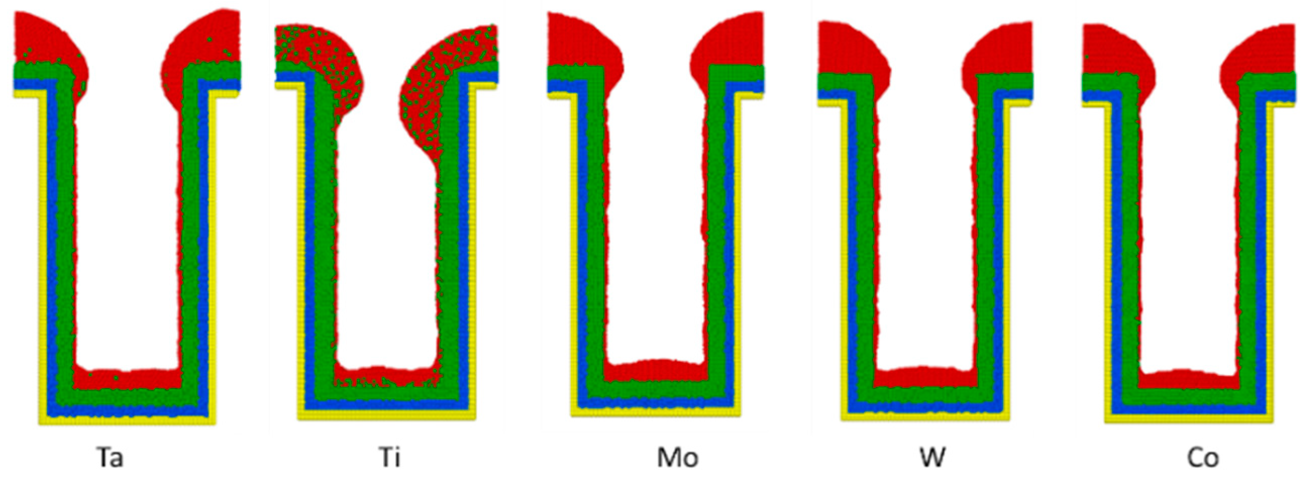
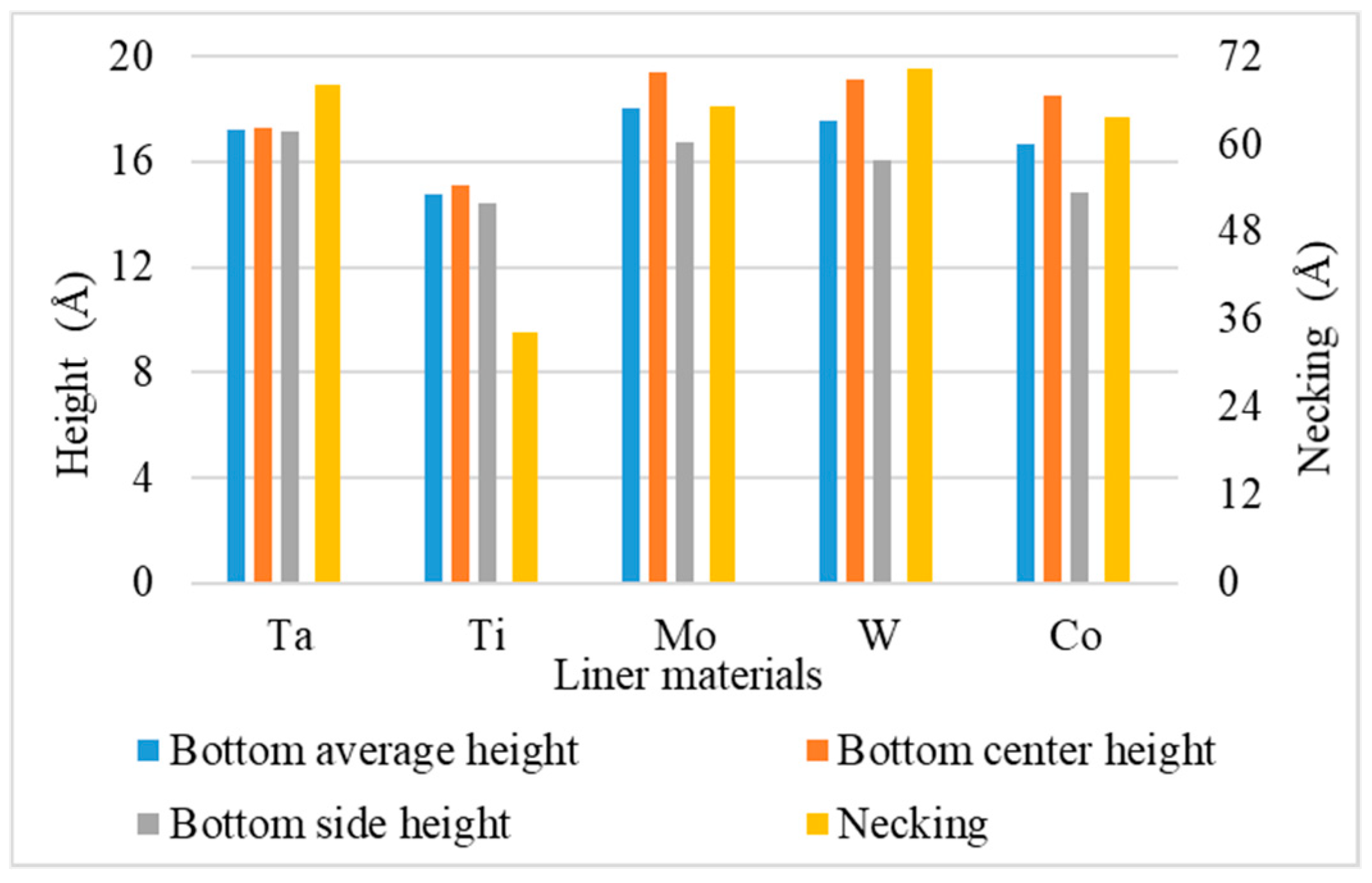
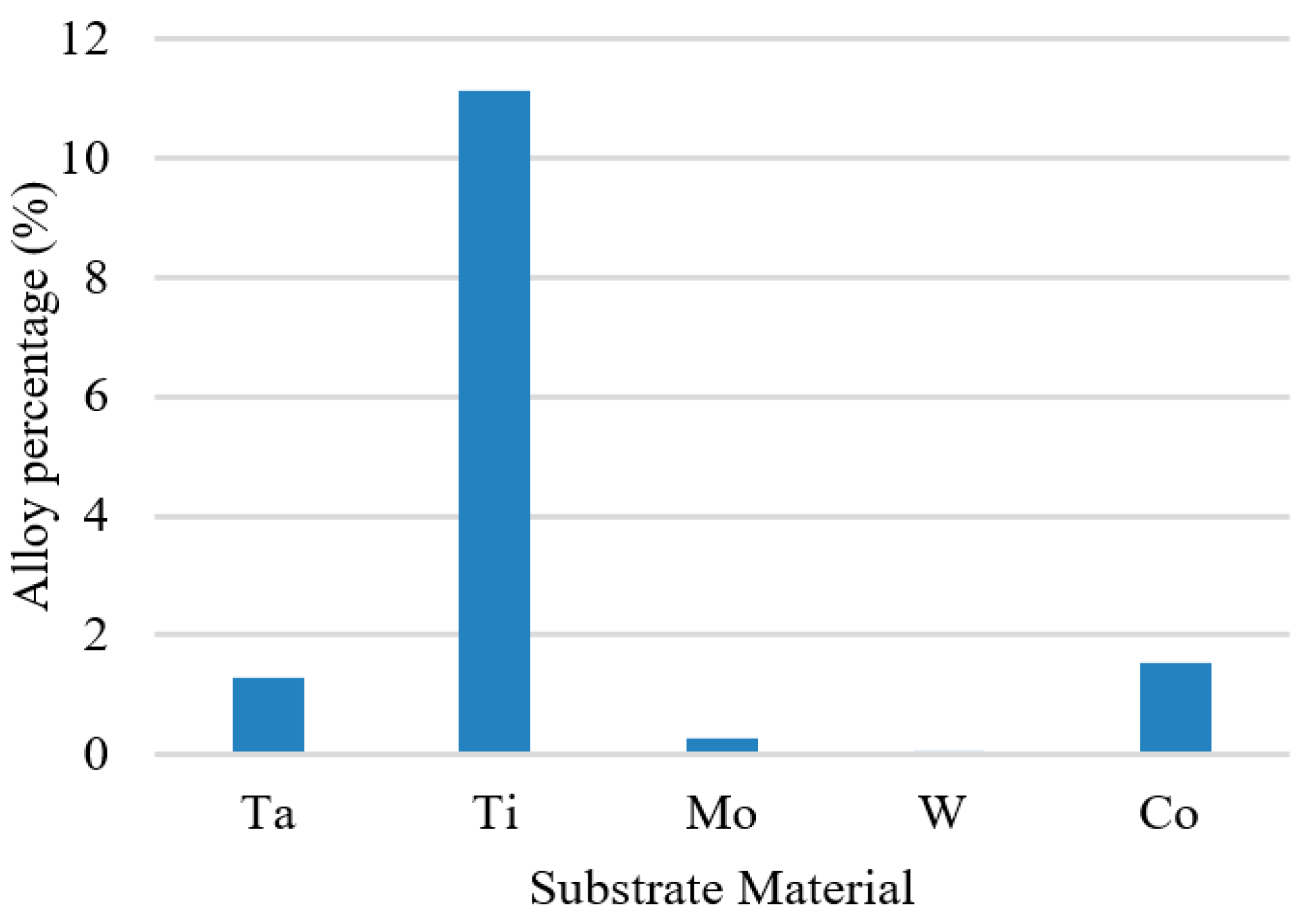
Each material has its unique properties that affect the quality of the copper seed layer. Parameters including surface energy, cohesive energy, interatomic potential, and lattice spacing are considered to be related. In this study, tantalum (Ta), titanium (Ti), molybdenum (Mo), tungsten (W), and cobalt (Co) were selected as the substrate material, while the other parameters were as follows: incident energy = 5 ev, deposition height = 5000 Å, incident angle = 30°, deposition rate = 10 atoms/ps, and substrate temperature = 600 K. The copper seed layer with different substrate materials is shown in Figure 34. The cohesive energy of titanium was low compared with tantalum, molybdenum, and tungsten. Moreover, its lattice spacing was larger than cobalt. Low cohesive energy means that it was easy to break the bond of titanium, while larger lattice spacing means that the incident copper was more likely to impact deeper into the substrate, transferring more energy to the substrate atoms; these mechanisms resulted in the largest alloy percentage of titanium. The best step coverage of different liner materials belonged to titanium, as illustrated in Figure 35.
The potential of pure copper is lower than the alloy potential, which means the alloy leads to an increase in diffusion barrier energy of copper atoms. Thus, the titanium alloy atoms of the copper seed layer caused the diffusivity to decrease, which decreased the diffusion of the atoms on the top sidewall to the wing. Atoms would then accumulate at the top sidewall and result in decreasing necking and uniformity.
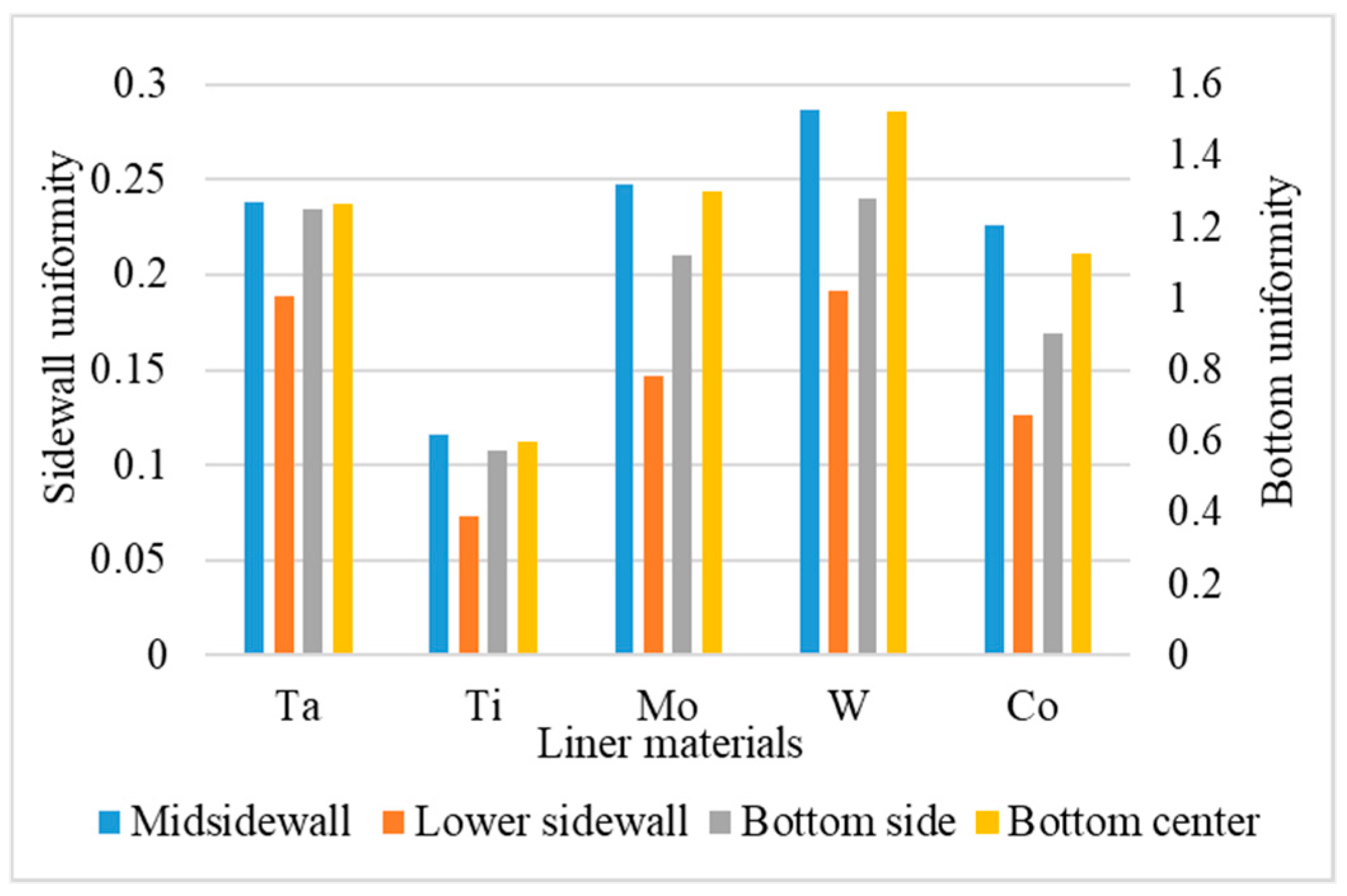
Tungsten had the best uniformity among the liner materials discussed in this study, as shown in Figure 36. The cohesive energy of tungsten was the largest, meaning that it was difficult to break the bonding of tungsten. This led to the lowest alloy percentage of tungsten. Without the effect of dragging diffusivity by alloy potential, the diffusivity of copper on tungsten substrates was larger than on other substrate materials, making the atoms at the top side wall easier to diffuse to the wing. This caused a decrease of the number of atoms at the top sidewall and an increase of necking as well as uniformity. Figure 37 shows the corresponding bottom height and necking of different substrate materials. The alloy percentage with different substrate materials is illustrated in Figure 38. In general, a larger cohesive energy, surface energy with lower lattice spacing, interatomic potential, and diffusion barrier energy leads to a better diffusion ability, which results in a more uniform copper seed layer.

4. Conclusions

The main objective of this study is to improve the quality of the copper seed layer. The low step coverage caused by atoms accumulating at the top sidewall can eventually be improved by the chemical–mechanical planarization (CMP) process. However, the poor uniformity caused by atoms accumulating at the top sidewall can only be improved by re-sputter or thermal reflow, which is less effective than CMP at the wing. Thus, uniformity is considered as the priority goal in this study.
From the results and discussion, remarks for depositing the copper seed layer for the interconnect metallization process are as follows:
  • The additional energy of atoms, such as increasing substrate temperature and increasing incident energy, leads the atoms at the wing to flow into the trench and mainly accumulate at the top sidewall. This increases the step coverage but decreases the uniformity.
  • Decreasing the deposition rate results in a better diffusion of deposited atoms to the substrate, thus increasing the effect of Ostwald ripening, which leads to better uniformity.
  • Different sections of the trench have optimal incident angles for receiving atoms, which are dependent on the size and features of the trench.
  • The necking of the copper seed layer can be increased by decreasing the substrate temperature, incident energy, incident angle, and deposition rate.
  • The overall bottom height of the copper seed layer can be increased by increasing the incident energy and decreasing the substrate temperature, incident angle, and deposition rate.
  • The alloy percentage can be decreased by decreasing the substrate temperature, incident energy, and deposition rate.
  • Surface diffusion barrier energy caused by the potential energy and lattice structure is the dominant factor of different crystal planes. A lower diffusion barrier energy at the sidewall direction of the trench with a larger diffusion barrier energy at the wing direction of the trench allows the atoms at the top sidewall to flow to the wing, while stopping atoms from flowing the other way. This increases the necking and leads to better uniformity.
  • For different liner materials, the alloy percentage of the copper seed layer is the dominant factor. With greater cohesive energy, the alloy percentage decreases and thus decreases the additional diffusion barrier energy from the alloy atoms, which results in atoms at the top sidewall flowing towards the wing. Consequently, the necking and uniformity are increased.
  • The wing and top sidewall are the dominant areas of the copper seed layer. If the atoms tend to flow from the top sidewall to the wing rather than the other way around, necking would increase. Atoms depositing into the trench would thus increase and result in better uniformity.
  • Among the parameters discussed in this study, the diffusion barrier of different crystal planes is the most decisive factor, which leads to good uniformity.
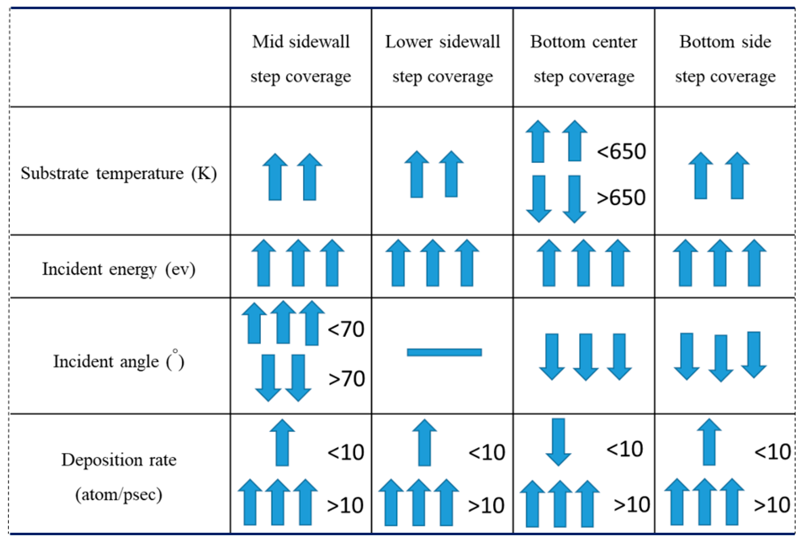
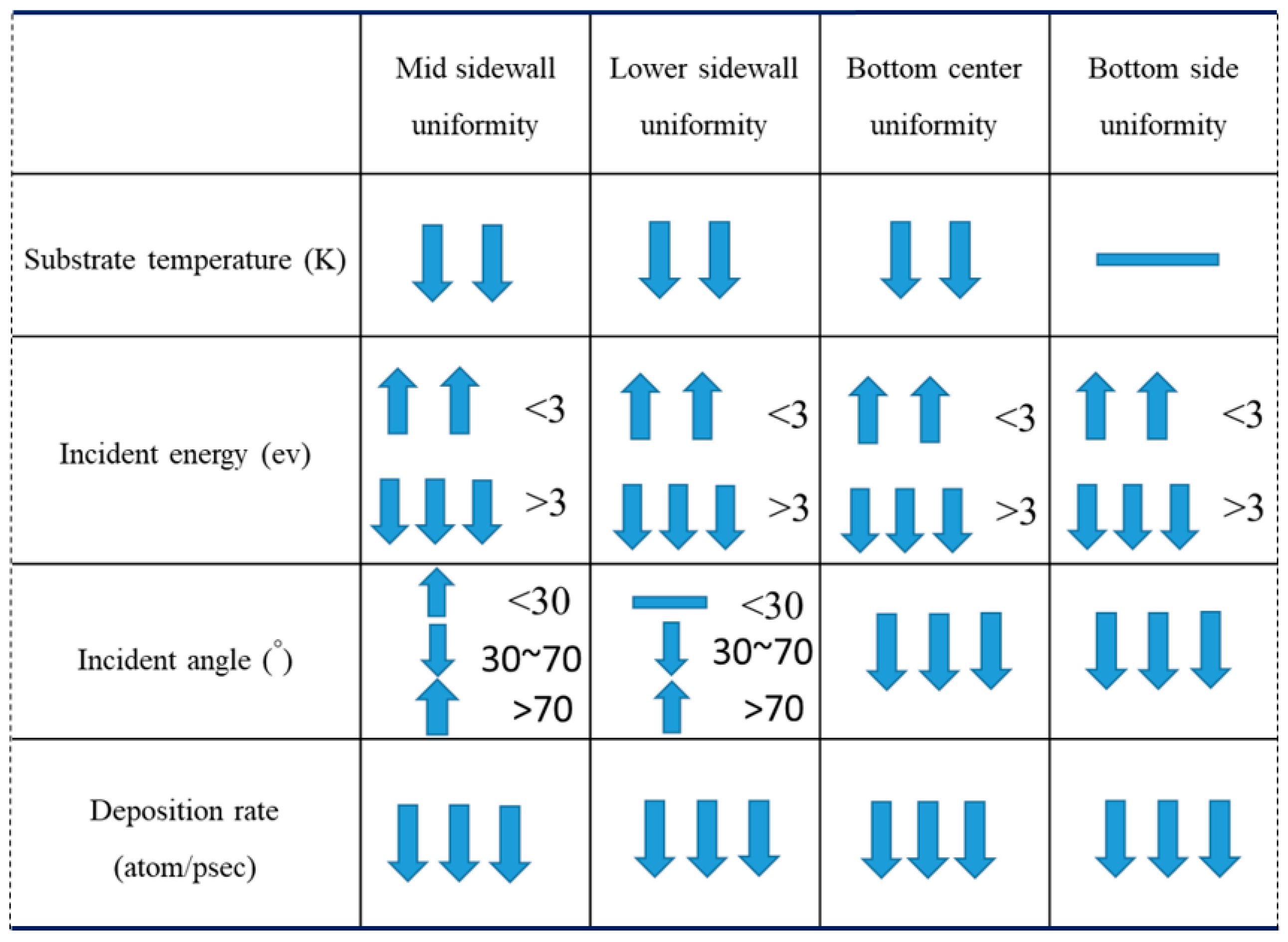
In general, optimization of process parameters and material properties requires online tuning to obtain the best quality copper seed layer under different circumstances. Based on the obtained results, valuable trend charts are developed for tuning recipe while depositing the copper seed layer. Crucial characteristics for evaluating the copper seed layer regarding different process parameters are included in the trend charts shown in Figure 39, Figure 40 and Figure 41, where up and down arrows denote positive and negative correlations, respectively, and the number of arrows indicates the strength of the correlation. It should be noted that the trends shown in the results are not always linear and might differ under different conditions.

Author Contributions

Conceptualization, C.-H.H., C.-K.C. and C.-L.C.; methodology, C.-K.C.; software, C.-H.H.; validation, C.-L.C. and C.-K.C.; formal analysis, C.-H.H.; data curation, C.-H.H.; writing—original draft preparation, C.-H.H. and C.-L.C.; writing—review and editing, C.-L.C.; supervision, C.-K.C.; funding acquisition, C.-L.C. All authors have read and agreed to the published version of the manuscript.

Funding

The work has been partly supported by the Ministry of Science and Technology, Taiwan, grant No. 106-2221-E-006-146.

Institutional Review Board Statement

Not applicable.

Informed Consent Statement

Not applicable.

Data Availability Statement

Not applicable.

Conflicts of Interest

The authors declare no conflict of interest.

References

  1. Motegi, N.; Kashimoto, Y.; Nagatani, K.; Takahashi, S.; Kondo, T.; Mizusawa, Y.; Nakayama, I. Long-throw low-pressure sputtering technology for very large-scale integrated devices. J. Vac. Sci. Technol. B 1995, 13, 1906–1909. [Google Scholar] [CrossRef]
  2. Rossnagel, S.M.; Mikalsen, D.; Kinoshita, H.; Cuomo, J.J. Collimated magnetron sputter deposition. J. Vac. Sci. Technol. A 1991, 9, 261–265. [Google Scholar] [CrossRef]
  3. Rossnagel, S.M.; Hopwood, J. Metal ion deposition from ionized magnetron sputtering discharge. J. Vac. Sci. Technol. B 1994, 12, 449–453. [Google Scholar] [CrossRef]
  4. Hopwood, J. Ionized physical vapor deposition of integrated circuit interconnects. Phys. Plasmas 1998, 5, 1624–1631. [Google Scholar] [CrossRef] [Green Version]
  5. Edelstein, D.; Uzoh, C.; Cabral, C., Jr.; DeHaven, P.; Buchwalter, P.; Simon, A. An optimal liner for copper damascene interconnects. In Proceedings of the Advanced Metallization Conference, Montreal, QC, Canada, 7–10 October 2001; pp. 541–547. [Google Scholar]
  6. Wu, W.; Wu, H.J.; Dixit, G.; Shaviv, R.; Gao, M.; Mountsier, T. Ti-based barrier for Cu interconnect applications. In Proceedings of the IEEE International Interconnect Technology Conference, Burlingame, CA, USA, 1–4 June 2008; pp. 202–204. [Google Scholar]
  7. Lanzillo, N.A.; Yang, C.C.; Motoyama, K.; Huang, H.; Cheng, K.; Maniscalco, J.; Van Der Straten, O.; Penny, C.; Standaert, T.; Choi, K. Exploring the Limits of Cobalt Liner Thickness in Advanced Copper Interconnects. IEEE Electron Device Lett. 2019, 40, 1804–1807. [Google Scholar] [CrossRef]
  8. Zhao, B.; Sun, K.; Song, Z.; Yang, J. Ultrathin Mo/MoN bilayer nanostructure for diffusion barrier application of advanced Cu metallization. Appl. Surf. Sci. 2010, 256, 6003–6006. [Google Scholar] [CrossRef]
  9. Ono, H.; Nakano, T.; Ohta, T. Diffusion Barrier Effects Against Cu of W-N Layer Formed by Electron Cyclotron Resonance Plasma Nitridation on W Layer. Jpn. J. Appl. Phys. 1995, 34, 1827–1830. [Google Scholar] [CrossRef]
  10. Yang, Y.G.; Zhou, X.W.; Johnson, R.A.; Wadley, H.G. Atomistic Simulations of Deep Submicron Interconnect Metallization. J. Vac. Sci. Technol. B 2002, 20, 622–630. [Google Scholar] [CrossRef] [Green Version]
  11. Lu, J.; Kushnerb, M.J. Trench filling by ionized metal physical vapor deposition. J. Vac. Sci. Technol. A 2001, 19, 2652–2663. [Google Scholar] [CrossRef] [Green Version]
  12. Ju, S.P.; Weng, C.I.; Hwang, C.C. Damascene process simulation using molecular dynamics. J. Appl. Phys. 2002, 92, 7062–7069. [Google Scholar] [CrossRef]
  13. Hong, R.T.; Yang, J.Y. Molecular Dynamics Study on Enhanced Cu Coverage of Trench Filling with Low-Index Ta Surfaces. Jpn. J. Appl. Phys. 2012, 51, 06FF14-1–06FF14-6. [Google Scholar] [CrossRef]
  14. Chan, K.Y.; Teo, B.-S. Sputtering power and deposition pressure effects on the electrical and structural properties of copper thin films. J. Mater. Sci. 2005, 40, 5971–5981. [Google Scholar] [CrossRef]
  15. Adrien Chauvin, A.; Horak, L.; Duverger-Nédellec, E.; Dopita, M.; Tessier, P.-Y.; El Mel, A.-A. Effect of the substrate temperature during gold-copper alloys thin film deposition by magnetron co-sputtering on the dealloying process. Surf. Coat. Technol. 2020, 383, 125220. [Google Scholar] [CrossRef]
  16. Li, Z.; Tian, Y.; Teng, C.; Cao, H. Recent Advances in Barrier Layer of Cu Interconnects. Materials 2020, 13, 5049. [Google Scholar] [CrossRef] [PubMed]
  17. Daw, M.S.; Baskes, M.I. Embedded-atom method: Derivation and application to impurities, surfaces, and other defects in metals. Phys. Rev. B 1984, 29, 6443–6453. [Google Scholar] [CrossRef] [Green Version]
  18. Johnson, R.A. Alloy Models with the Embedded-Atom Method. Phys. Rev. B 1989, 39, 12554–12559. [Google Scholar] [CrossRef] [PubMed]
  19. Zhou, X.W.; Johnson, R.A.; Wadley, H.N.G. Misfit-energy-increasing dislocations in vapor-deposited CoFe/NiFe multilayers. Phys. Rev. B 2004, 69, 144113. [Google Scholar] [CrossRef] [Green Version]
  20. Langevin, P. On the theory of Brownian motion. C. R. Acad. Sci. 1908, 146, 530–533. [Google Scholar]
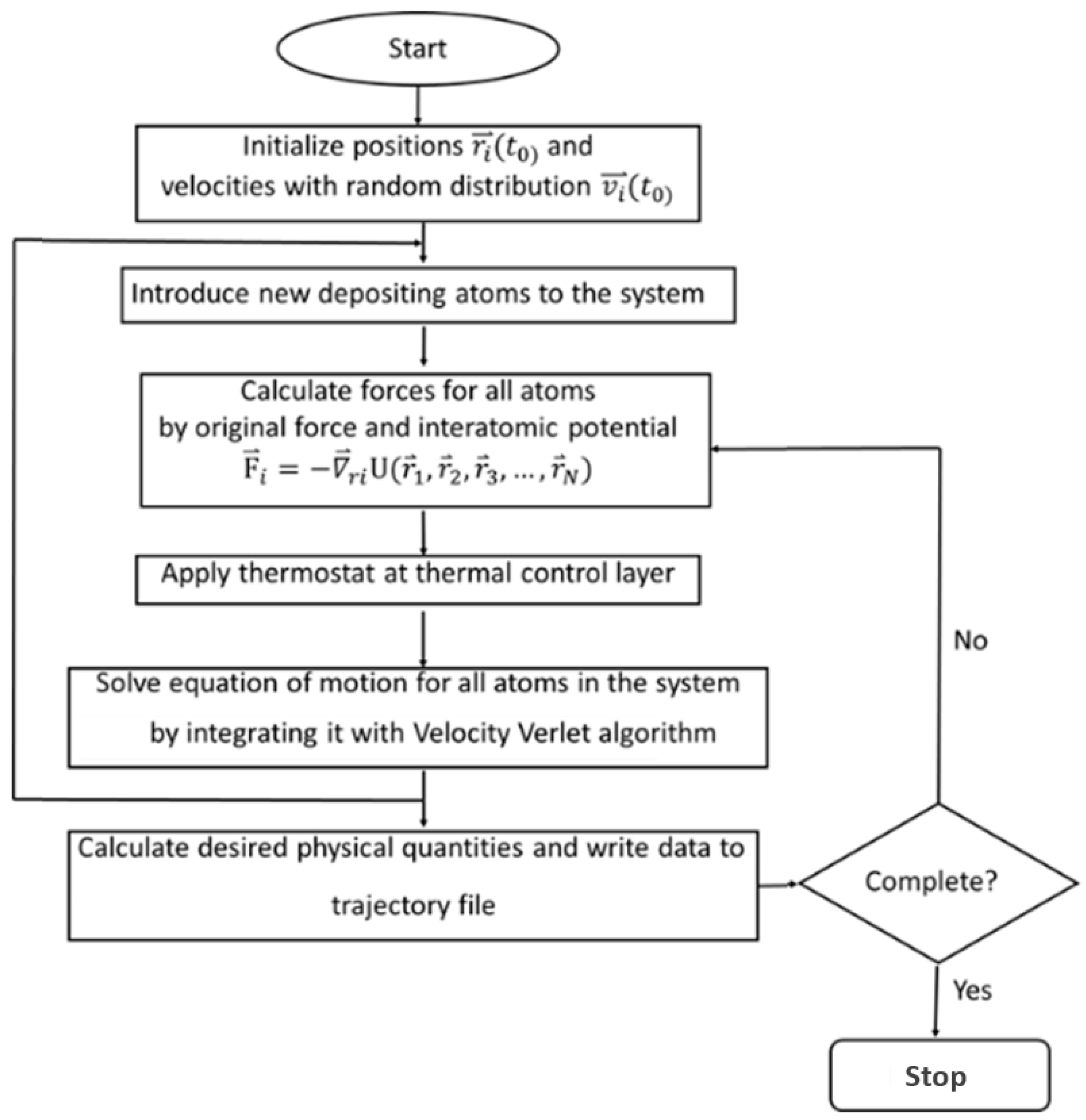
Figure 1. Flow chart of molecular dynamics simulation.
Applsci 11 09702 g001
Figure 2. Model of substrate trench.
Applsci 11 09702 g002
Figure 3. Model of copper deposition into substrate trench with cosine distribution of incident copper atoms.
Applsci 11 09702 g003
Figure 4. Defined regions of the trench model.
Applsci 11 09702 g004
Figure 5. Copper seed layers under different substrate temperatures.
Applsci 11 09702 g005
Figure 6. Overall distribution of the deposited copper atoms with respect to substrate temperatures.
Applsci 11 09702 g006
Figure 7. Step coverage with different substrate temperatures.
Applsci 11 09702 g007
Figure 8. Uniformity with different substrate temperatures.
Applsci 11 09702 g008
Figure 9. Bottom height and necking with different substrate temperatures.
Applsci 11 09702 g009
Figure 10. Alloy percentage with different substrate temperatures.
Applsci 11 09702 g010
Figure 11. Copper seed layer with different incident energy.
Applsci 11 09702 g011
Figure 12. Overall distribution of the deposited copper atoms with respect to incident energy.
Applsci 11 09702 g012
Figure 13. Bottom height and necking with different incident energy.
Applsci 11 09702 g013
Figure 14. Step coverage with different incident energy.
Applsci 11 09702 g014
Figure 15. Uniformity with different incident energy.
Applsci 11 09702 g015
Figure 16. Alloy percentage with different incident energy.
Applsci 11 09702 g016
Figure 17. Copper seed layer with different incident angles.
Applsci 11 09702 g017
Figure 18. Overall distribution of the deposited copper atoms with respect to incident angles.
Applsci 11 09702 g018
Figure 19. Step coverage with different incident angles.
Applsci 11 09702 g019
Figure 20. Uniformity with different incident angles.
Applsci 11 09702 g020
Figure 21. Bottom height and necking with different incident angles.
Applsci 11 09702 g021
Figure 22. Alloy percentage with different incident angles.
Applsci 11 09702 g022
Figure 23. Copper seed layer with different deposition rates.
Applsci 11 09702 g023
Figure 24. Overall distribution of the deposited copper atoms with respect to deposition rates.
Applsci 11 09702 g024
Figure 25. Step coverage with different deposition rates.
Applsci 11 09702 g025
Figure 26. Uniformity with different deposition rates.
Applsci 11 09702 g026
Figure 27. Bottom height and necking with different deposition rates.
Applsci 11 09702 g027
Figure 28. Alloy percentage with different deposition rates.
Applsci 11 09702 g028
Figure 29. Copper seed layer with different crystal planes.
Applsci 11 09702 g029
Figure 30. Step coverage with different crystal planes.
Applsci 11 09702 g030
Figure 31. Uniformity with different crystal planes.
Applsci 11 09702 g031
Figure 32. Bottom height and necking with different crystal planes.
Applsci 11 09702 g032
Figure 33. Alloy percentage with different crystal planes.
Applsci 11 09702 g033
Figure 34. Copper seed layer with different substrate materials.
Applsci 11 09702 g034
Figure 35. Step coverage with different substrate materials.
Applsci 11 09702 g035
Figure 36. Uniformity with different substrate materials.
Applsci 11 09702 g036
Figure 37. Bottom height and necking with different substrate materials.
Applsci 11 09702 g037
Figure 38. Alloy percentage with different substrate materials.
Applsci 11 09702 g038
Figure 39. Trend chart of sputtering process parameters and step coverage.
Applsci 11 09702 g039
Figure 40. Trend chart of sputtering process parameters and uniformity.
Applsci 11 09702 g040
Figure 41. Trend chart of sputtering process parameters and quality of copper seed layer.
Applsci 11 09702 g041
Table 1. Crystal structure and lattice parameters of different materials.
MaterialsCrystal StructureLattice Parameters (Angstroms)
Tantalum (Ta)BCC3.3, 3.3, 3.3
Titanium (Ti)HCP2.95, 2.95, 4.68
Molybdenum (Mo)BCC3.147, 3.147, 3.147
Cobalt (Co)HCP2.51, 2.51, 4.07
Tungsten (W)BCC3.17, 3.17, 3.17
Table 2. Diffusion barrier energy on different crystal planes of tantalum [13].
SurfaceLayersSurface Diffusion Barrier Energy (ev)
Ta (100)160.883
Ta (110)140.543
Ta (111)142.076
Publisher’s Note: MDPI stays neutral with regard to jurisdictional claims in published maps and institutional affiliations.