
In-Plane Monolithic Integration of Scaled III-V Photonic Devices

 , , and
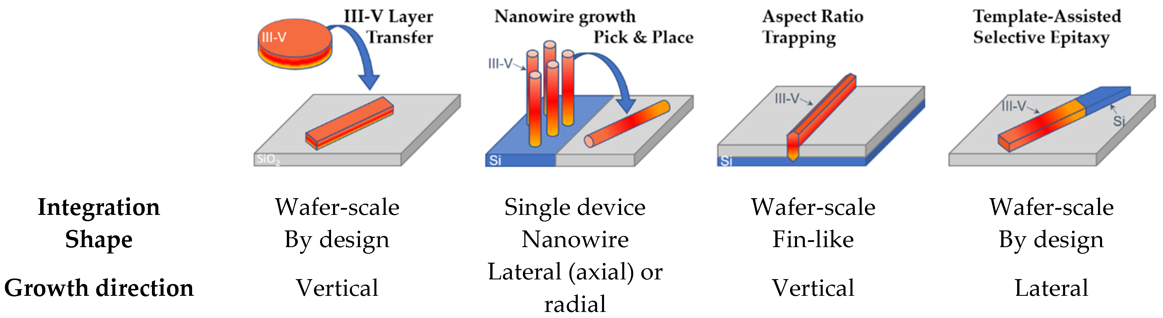
Abstract
:1. Introduction
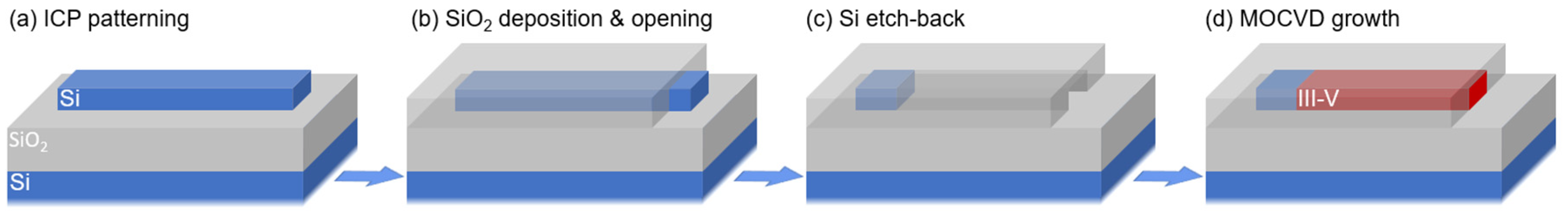
2. Template-Assisted Selective Epitaxy
3. Hybrid III-V/Si Photonic Crystal Cavity Lasers
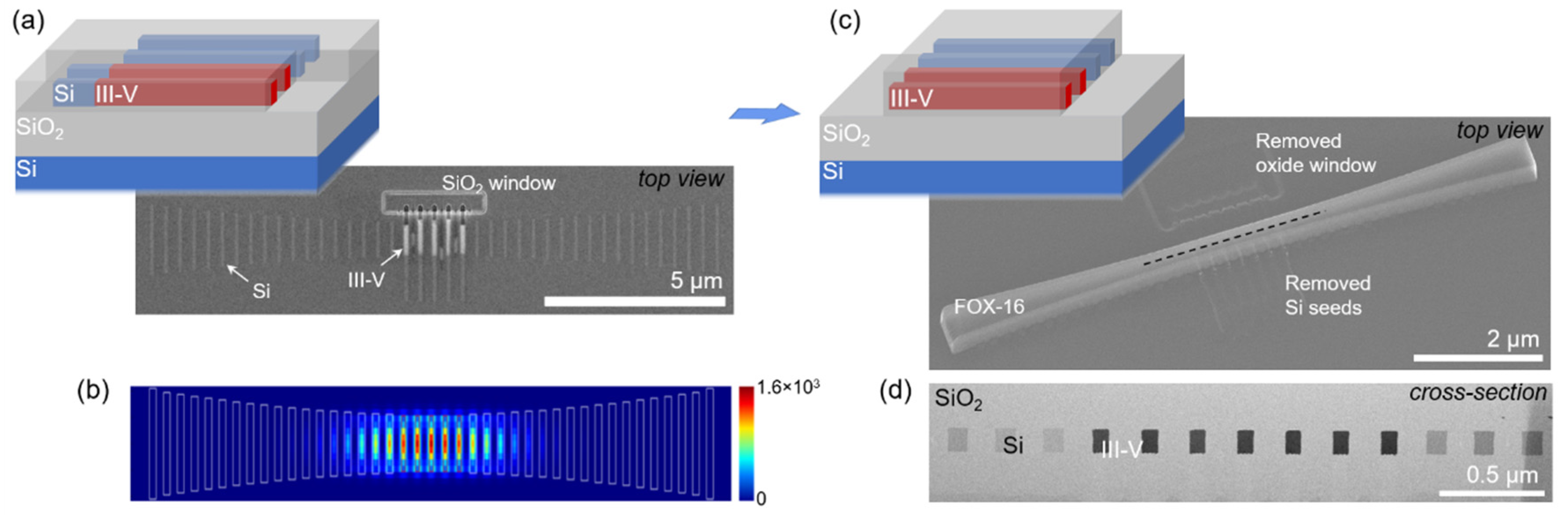
3.1. Design and Fabrication
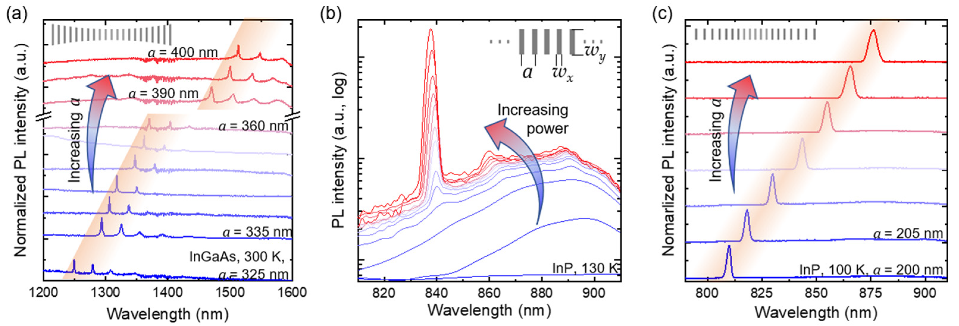
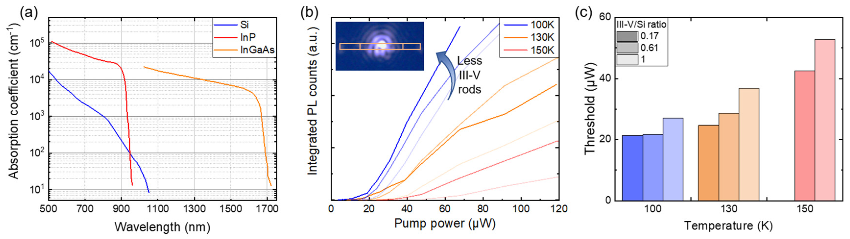
3.2. Characterization of Hybrid III-V/Si PhC Cavities
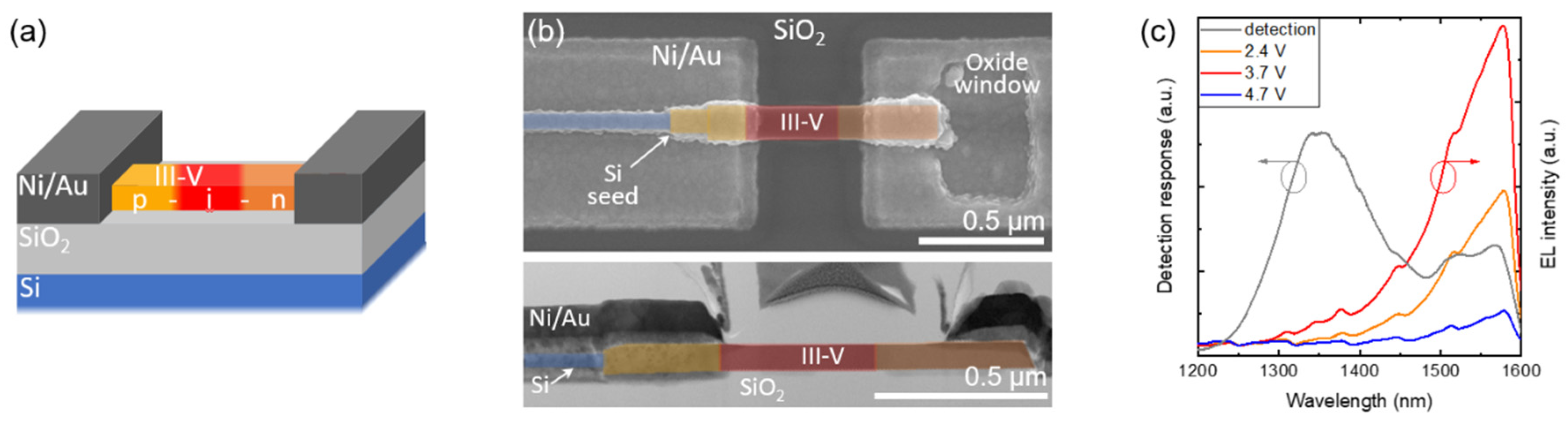
4. Monolithic Detectors
5. Conclusions
Author Contributions
Funding
Data Availability Statement
Acknowledgments
Conflicts of Interest
References
- Rahim, A.; Goyvaerts, J.; Szelag, B.; Fedeli, J.; Absil, P.; Aalto, T.; Harjanne, M.; Littlejohns, C.; Reed, G.; Winzer, G.; et al. Open-Access Silicon Photonics Platforms in Europe. IEEE J. Sel. Top. Quantum Electron. 2019, 25, 1–18. [Google Scholar] [CrossRef] [Green Version]
- Miller, S.A.; Yu, M.; Ji, X.; Griffith, A.G.; Cardenas, J.; Gaeta, A.L.; Lipson, M. Low-Loss Silicon Platform for Broadband Mid-Infrared Photonics. Optica 2017, 4, 707–712. [Google Scholar] [CrossRef]
- Crosnier, G.; Sanchez, D.; Bouchoule, S.; Monnier, P.; Beaudoin, G.; Sagnes, I.; Raj, R.; Raineri, F. Hybrid Indium Phosphide-on-Silicon Nanolaser Diode. Nat. Photonics 2017, 11, 297–300. [Google Scholar] [CrossRef]
- Tanabe, K.; Watanabe, K.; Arakawa, Y. III-V/Si Hybrid Photonic Devices by Direct Fusion Bonding. Sci. Rep. 2012, 2. [Google Scholar] [CrossRef] [PubMed]
- Hu, Y.; Liang, D.; Mukherjee, K.; Li, Y.; Zhang, C.; Kurczveil, G.; Huang, X.; Beausoleil, R.G. III/V-on-Si MQW Lasers by Using a Novel Photonic Integration Method of Regrowth on a Bonding Template. Light Sci. Appl. 2019, 8, 93. [Google Scholar] [CrossRef]
- Duprez, H.; Descos, A.; Ferrotti, T.; Sciancalepore, C.; Jany, C.; Hassan, K.; Seassal, C.; Menezo, S.; Bakir, B.B. 1310nm Hybrid InP/InGaAsP on Silicon Distributed Feedback Laser with High Side-Mode Suppression Ratio. Opt. Express OE 2015, 23, 8489–8497. [Google Scholar] [CrossRef] [PubMed]
- Fang, A.W.; Park, H.; Cohen, O.; Jones, R.; Paniccia, M.J.; Bowers, J.E. Electrically Pumped Hybrid AlGaInAs-Silicon Evanescent Laser. Opt. Express OE 2006, 14, 9203–9210. [Google Scholar] [CrossRef]
- Keyvaninia, S.; Muneeb, M.; Stankovic, S.; Veldhoven, P.J.; Thourhout, D.; Roelkens, G. Ultra-Thin DVS-BCB Adhesive Bonding of III-V Wafers, Dies and Multiple Dies to a Patterned Silicon-on-Insulator Substrate. Opt. Mater. Express 2013, 3. [Google Scholar] [CrossRef] [Green Version]
- Luo, X.; Cao, Y.; Song, J.; Hu, X.; Cheng, Y.; Li, C.; Liu, C.; Liow, T.-Y.; Yu, M.; Wang, H.; et al. High-Throughput Multiple Dies-to-Wafer Bonding Technology and III/V-on-Si Hybrid Lasers for Heterogeneous Integration of Optoelectronic Integrated Circuits. Front. Mater. 2015, 2. [Google Scholar] [CrossRef] [Green Version]
- Baumgartner, Y.; Caimi, D.; Sousa, M.; Hopstaken, M.; Salamin, Y.; Baeuerle, B.; Bitachon, B.I.; Leuthold, J.; Faist, J.; Offrein, B.J.; et al. High-Speed CMOS-Compatible III-V on Si Membrane Photodetectors. Opt. Express OE 2021, 29, 509–516. [Google Scholar] [CrossRef]
- Zhang, J.; De Groote, A.; Abbasi, A.; Loi, R.; O’Callaghan, J.; Corbett, B.; Trindade, A.J.; Bower, C.A.; Roelkens, G. Silicon Photonics Fiber-to-the-Home Transceiver Array Based on Transfer-Printing-Based Integration of III-V Photodetectors. Opt. Express 2017, 25, 14290. [Google Scholar] [CrossRef] [PubMed] [Green Version]
- Bower, C.A.; Bonafede, S.; Radauscher, E.; Pearson, A.; Raymond, B.; Vick, E.; Verreen, C.; Weeks, T.; Krongard, B.; Meitl, M. Emissive Displays with Transfer-Printed Microscale LEDs and ICs. In Proceedings of the Light-Emitting Devices, Materials, and Applications XXIV, San Francisco, CA, USA, 1–6 February 2020; Strassburg, M., Kim, J.K., Krames, M.R., Eds.; SPIE: San Francisco, CA, USA, 2020. [Google Scholar]
- Mayer, B.; Janker, L.; Loitsch, B.; Treu, J.; Kostenbader, T.; Lichtmannecker, S.; Reichert, T.; Morkötter, S.; Kaniber, M.; Abstreiter, G.; et al. Monolithically Integrated High-β Nanowire Lasers on Silicon. Nano Lett. 2016, 16, 152–156. [Google Scholar] [CrossRef]
- Tomioka, K.; Motohisa, J.; Fukui, T. Rational Synthesis of Atomically Thin Quantum Structures in Nanowires Based on Nucleation Processes. Sci. Rep. 2020, 10, 10720. [Google Scholar] [CrossRef]
- Kim, H.; Lee, W.-J.; Farrell, A.C.; Balgarkashi, A.; Huffaker, D.L. Telecom-Wavelength Bottom-up Nanobeam Lasers on Silicon-on-Insulator. Nano Lett. 2017, 17, 5244–5250. [Google Scholar] [CrossRef] [Green Version]
- Chang, T.; Kim, H.; Zutter, B.T.; Lee, W.; Regan, B.C.; Huffaker, D.L. Orientation-Controlled Selective-Area Epitaxy of III–V Nanowires on (001) Silicon for Silicon Photonics. Adv. Funct. Mater. 2020, 30, 2002220. [Google Scholar] [CrossRef]
- Rothman, A.; Dubrovskii, V.G.; Joselevich, E. Kinetics and Mechanism of Planar Nanowire Growth. PNAS 2020, 117, 152–160. [Google Scholar] [CrossRef]
- Fortuna, S.A.; Li, X. GaAs MESFET With a High-Mobility Self-Assembled Planar Nanowire Channel. IEEE Electron Device Lett. 2009, 30, 593–595. [Google Scholar] [CrossRef]
- Pozina, G.; Gubaydullin, A.R.; Mitrofanov, M.I.; Kaliteevski, M.A.; Levitskii, I.V.; Voznyuk, G.V.; Tatarinov, E.E.; Evtikhiev, V.P.; Rodin, S.N.; Kaliteevskiy, V.N.; et al. Approach to High Quality GaN Lateral Nanowires and Planar Cavities Fabricated by Focused Ion Beam and Metal-Organic Vapor Phase Epitaxy. Sci. Rep. 2018, 8, 7218. [Google Scholar] [CrossRef] [PubMed] [Green Version]
- Takiguchi, M.; Yokoo, A.; Nozaki, K.; Birowosuto, M.D.; Tateno, K.; Zhang, G.; Kuramochi, E.; Shinya, A.; Notomi, M. Continuous-Wave Operation and 10-Gb/s Direct Modulation of InAsP/InP Sub-Wavelength Nanowire Laser on Silicon Photonic Crystal. APL Photonics 2017, 2, 046106. [Google Scholar] [CrossRef] [Green Version]
- Takiguchi, M.; Sasaki, S.; Tateno, K.; Chen, E.; Nozaki, K.; Sergent, S.; Kuramochi, E.; Zhang, G.; Shinya, A.; Notomi, M. Hybrid Nanowire Photodetector Integrated in a Silicon Photonic Crystal. ACS Photonics 2020, 7, 3467–3473. [Google Scholar] [CrossRef]
- Vais, A.; Witters, L.; Mols, Y.; Hernandez, A.S.; Walke, A.; Yu, H.; Baryshnikova, M.; Mannaert, G.; Deshpande, V.; Alcotte, R.; et al. First Demonstration of III-V HBTs on 300mm Si Substrates Using Nano-Ridge Engineering. In Proceedings of the 2019 IEEE International Electron Devices Meeting (IEDM), San Francisco, CA, USA, 7–11 December 2019; pp. 9.1.1–9.1.4. [Google Scholar]
- Kunert, B.; Guo, W.; Mols, Y.; Tian, B.; Wang, Z.; Shi, Y.; Van Thourhout, D.; Pantouvaki, M.; Van Campenhout, J.; Langer, R.; et al. III/V Nano Ridge Structures for Optical Applications on Patterned 300mm Silicon Substrate. Appl. Phys. Lett. 2016, 109, 091101. [Google Scholar] [CrossRef]
- Shi, Y.; Wang, Z.; Campenhout, J.V.; Pantouvaki, M.; Guo, W.; Kunert, B.; Thourhout, D.V. Optical Pumped InGaAs/GaAs Nano-Ridge Laser Epitaxially Grown on a Standard 300mm Si Wafer. Optica 2017, 4, 1468–1473. [Google Scholar] [CrossRef]
- Han, Y.; Ng, W.K.; Ma, C.; Li, Q.; Zhu, S.; Chan, C.C.S.; Ng, K.W.; Lennon, S.; Taylor, R.A.; Wong, K.S.; et al. Room-Temperature InP/InGaAs Nano-Ridge Lasers Grown on Si and Emitting at Telecom Bands. Optica 2018, 5, 918. [Google Scholar] [CrossRef]
- Han, Y.; Yan, Z.; Ng, W.K.; Xue, Y.; Wong, K.S.; Lau, K.M. Bufferless 1.5µm III-V Lasers Grown on Si-Photonics 220nm Silicon-on-Insulator Platforms. Optica 2020, 7, 148–153. [Google Scholar] [CrossRef]
- Matsuo, S.; Takeda, K. λ-Scale Embedded Active Region Photonic Crystal (LEAP) Lasers for Optical Interconnects. Photonics 2019, 6, 82. [Google Scholar] [CrossRef] [Green Version]
- Schmid, H.; Borg, M.; Moselund, K.; Gignac, L.; Breslin, C.M.; Bruley, J.; Cutaia, D.; Riel, H. Template-Assisted Selective Epitaxy of III–V Nanoscale Devices for Co-Planar Heterogeneous Integration with Si. Appl. Phys. Lett. 2015, 106, 233101. [Google Scholar] [CrossRef]
- Borg, M.; Gignac, L.; Bruley, J.; Malmgren, A.; Sant, S.; Convertino, C.; Rossell, M.D.; Sousa, M.; Breslin, C.; Riel, H.; et al. Facet-Selective Group-III Incorporation in InGaAs Template Assisted Selective Epitaxy. Nanotechnology 2018, 30, 084004. [Google Scholar] [CrossRef]
- Cutaia, D.; Moselund, K.E.; Schmid, H.; Borg, M.; Olziersky, A.; Riel, H. Complementary III–V Heterojunction Lateral NW Tunnel FET Technology on Si. In Proceedings of the 2016 IEEE Symposium on VLSI Technology, Honolulu, HI, USA, 14–16 June 2016; pp. 1–2. [Google Scholar]
- Mauthe, S.; Vico Triviño, N.; Baumgartner, Y.; Sousa, M.; Caimi, D.; Stöferle, T.; Schmid, H.; Moselund, K.E. InP-on-Si Optically Pumped Microdisk Lasers via Monolithic Growth and Wafer Bonding. IEEE J. Sel. Top. Quantum Electron. 2019, 25, 1–7. [Google Scholar] [CrossRef]
- Mayer, B.F.; Wirths, S.; Mauthe, S.; Staudinger, P.; Sousa, M.; Winiger, J.; Schmid, H.; Moselund, K.E. Microcavity Lasers on Silicon by Template-Assisted Selective Epitaxy of Microsubstrates. IEEE Photonics Technol. Lett. 2019, 31, 1021–1024. [Google Scholar] [CrossRef]
- Mauthe, S.; Tiwari, P.; Scherrer, M.; Caimi, D.; Sousa, M.; Schmid, H.; Moselund, K.E.; Vico Triviño, N. Hybrid III–V Silicon Photonic Crystal Cavity Emitting at Telecom Wavelengths. Nano Lett. 2020, 20, 8768–8772. [Google Scholar] [CrossRef]
- Mauthe, S.; Baumgartner, Y.; Sousa, M.; Ding, Q.; Rossell, M.D.; Schenk, A.; Czornomaz, L.; Moselund, K.E. High-Speed III-V Nanowire Photodetector Monolithically Integrated on Si. Nat. Commun. 2020, 11, 4565. [Google Scholar] [CrossRef] [PubMed]
- Bologna, N.; Wirths, S.; Francaviglia, L.; Campanini, M.; Schmid, H.; Theofylaktopoulos, V.; Moselund, K.E.; Fontcuberta i Morral, A.; Erni, R.; Riel, H.; et al. Dopant-Induced Modifications of GaxIn(1–x)P Nanowire-Based p–n Junctions Monolithically Integrated on Si(111). ACS Appl. Mater. Interfaces 2018, 10, 32588–32596. [Google Scholar] [CrossRef]
- Mauthe, S.; Baumgartner, Y.; Sant, S.; Ding, Q.; Sousa, M.; Czornomaz, L.; Schenk, A.; Moselund, K.E. Ultra-Thin III-V Photodetectors Epitaxially Integrated on Si with Bandwidth Exceeding 25 GHz. In Proceedings of the Optical Fiber Communication Conference (OFC) 2020 (2020), paper M3D.3, San Diego, CA, USA, 8–12 March 2020; Optical Society of America: Washington, DC, USA, 2020; p. M3D.3. [Google Scholar]
- Matsuo, S.; Shinya, A.; Chen, C.-H.; Nozaki, K.; Sato, T.; Kawaguchi, Y.; Taniyama, H.; Notomi, M. 20-Gbit/s Directly Modulated Photonic Crystal Nanocavity Laser with Ultra-Low Power Consumption. Opt. Express OE 2011, 19, 2242–2250. [Google Scholar] [CrossRef]
- Nozaki, K.; Matsuo, S.; Fujii, T.; Takeda, K.; Shinya, A.; Kuramochi, E.; Notomi, M. Femtofarad Optoelectronic Integration Demonstrating Energy-Saving Signal Conversion and Nonlinear Functions. Nat. Photonics 2019, 13, 454–459. [Google Scholar] [CrossRef]
- Crosnier, G.; Sanchez, D.; Bazin, A.; Monnier, P.; Bouchoule, S.; Braive, R.; Beaudoin, G.; Sagnes, I.; Raj, R.; Raineri, F. High Q Factor InP Photonic Crystal Nanobeam Cavities on Silicon Wire Waveguides. Opt. Lett. 2016, 41, 579. [Google Scholar] [CrossRef] [PubMed]
- Quan, Q.; Loncar, M. Deterministic Design of Wavelength Scale, Ultra-High Q Photonic Crystal Nanobeam Cavities. Opt. Express 2011, 19, 18529. [Google Scholar] [CrossRef] [PubMed] [Green Version]
- Sakanas, A.; Mathiesen, K.S.; Yu, Y.; Semenova, E.; Ottaviano, L.; Mork, J.; Yvind, K. Threshold Power Investigations of Optically-Pumped Photonic Crystal Lasers with Buried Heterostructure Gain Regions. In Proceedings of the 2019 Conference on Lasers and Electro-Optics Europe (CLEO/Europe), Munich, Germany, 23–27 June 2019; p. 1. [Google Scholar]
- Yao, K.; Shi, Y. High-Q Width Modulated Photonic Crystal Stack Mode-Gap Cavity and Its Application to Refractive Index Sensing. Opt. Express 2012, 20, 27039. [Google Scholar] [CrossRef]
- Green, M.A. Self-Consistent Optical Parameters of Intrinsic Silicon at 300 K Including Temperature Coefficients. Sol. Energy Mater. Sol. Cells 2008, 92, 1305–1310. [Google Scholar] [CrossRef]
- Palik, E.D. Handbook of Optical Constants of Solids; Academic Press: Boston, MA, USA, 1998; ISBN 978-0-12-544422-4. [Google Scholar]
- Poli, C.; Bellec, M.; Kuhl, U.; Mortessagne, F.; Schomerus, H. Selective Enhancement of Topologically Induced Interface States in a Dielectric Resonator Chain. Nat. Commun. 2015, 6, 6710. [Google Scholar] [CrossRef] [Green Version]
- Parto, M. Edge-Mode Lasing in 1D Topological Active Arrays. Phys. Rev. Lett. 2018, 120. [Google Scholar] [CrossRef] [Green Version]


Publisher’s Note: MDPI stays neutral with regard to jurisdictional claims in published maps and institutional affiliations. |
© 2021 by the authors. Licensee MDPI, Basel, Switzerland. This article is an open access article distributed under the terms and conditions of the Creative Commons Attribution (CC BY) license (http://creativecommons.org/licenses/by/4.0/).
Share and Cite
Scherrer, M.; Vico Triviño, N.; Mauthe, S.; Tiwari, P.; Schmid, H.; Moselund, K.E. In-Plane Monolithic Integration of Scaled III-V Photonic Devices. Appl. Sci. 2021, 11, 1887. https://doi.org/10.3390/app11041887
Scherrer M, Vico Triviño N, Mauthe S, Tiwari P, Schmid H, Moselund KE. In-Plane Monolithic Integration of Scaled III-V Photonic Devices. Applied Sciences. 2021; 11(4):1887. https://doi.org/10.3390/app11041887
Chicago/Turabian StyleScherrer, Markus, Noelia Vico Triviño, Svenja Mauthe, Preksha Tiwari, Heinz Schmid, and Kirsten E. Moselund. 2021. "In-Plane Monolithic Integration of Scaled III-V Photonic Devices" Applied Sciences 11, no. 4: 1887. https://doi.org/10.3390/app11041887