Article

An LLC Converter with Capacitive Insulation

1
Department of Ph.D. Program, Prospective Technology of Electrical Engineering and Computer Science, National Chin-Yi University of Technology, Taichung 41170, Taiwan
2
Department of Electrical Engineering, National Chin-Yi University of Technology, Taichung 41170, Taiwan
3
Asian Power Device Inc., Taoyuan 33058, Taiwan
*
Author to whom correspondence should be addressed.
Appl. Sci. 2022, 12(10), 4950; https://doi.org/10.3390/app12104950
Submission received: 13 April 2022 / Revised: 10 May 2022 / Accepted: 11 May 2022 / Published: 13 May 2022
(This article belongs to the Special Issue Advanced Power Converter and Applications in Electric Vehicles)

Abstract

:
Offline power converter products must apply for and pass the national electrical safety code before they can be marketed. The transformers of offline power converters must be made from certificated materials with a high voltage rating and high electrical insulation, which increases the volume of the transformers and the printed circuit boards. In most studies, the miniaturization of a power converter is usually achieved by increasing the conversion efficiency and reducing the heat sink, or by increasing the switching frequency to reduce the size of the transformers. In this paper, the insulation material is reduced to miniaturize the transformer of the LLC converter. The resonant capacitor of the LLC converter is used to meet the requirements of insulation voltage, leakage current, creepage, and clearance. A prototype with the specifications of 12 V and 10 A rated output was built to verify the proposed method.

1. Introduction

Offline power converter products must apply for and pass the national electrical safety code before they can be marketed. That means the transformer must be designed and manufactured with certified materials with high voltage rating and high electrical insulation. Therefore, the volume of the transformer and the printed circuit board (PCB) increase. In this paper, the insulation material is reduced to miniaturize the volume of the transformer of the LLC converter. The resonant capacitor of the LLC converter is used to meet the requirements of the electrical safety regulations.

1.1. Safety Capacitors

Typically, for offline converters, safety capacitors are required to suppress the conducted interference due to the electromagnetic interference (EMI) in the alternating current (AC) input. The AC power input is divided into three terminals: line, neutral, and earth ground. The safety capacitors in the line–earth or neutral–earth and the primary side to the secondary side are referred to as Y capacitors, and these capacitors should be certified for safety certification [1].
Y capacitors can be divided into four classes, Y1 to Y4, according to different withstand voltage levels. The smaller the number is, the higher the safety level, as shown in Table 1. Briefly, class Y1 and class Y2 are more commonly used: the Y2 capacitor, called Y2-cap, is used on line–earth or neutral–earth, and the Y1 capacitor, called Y1-cap, should be used on the primary side to the secondary side. In addition, the Y1 capacitor is marked with a rated withstand voltage of 250 V or 275 V. However, the peak pulse withstand voltage of the Y1 capacitor is as high as 8 kV, and the peak pulse withstand voltage of the Y2 capacitor is as high as 5 kV, as shown in Table 1.
Many previous studies have presented circuit architectures using Class Y capacitors as isolation components and these capacitors replace transformers as energy transfer components. However, this is only for LED lighting [2,3,4,5,6,7,8] or electric vehicle chargers [9,10], and is characterized by the fact that the secondary side is not in contact with the human body.

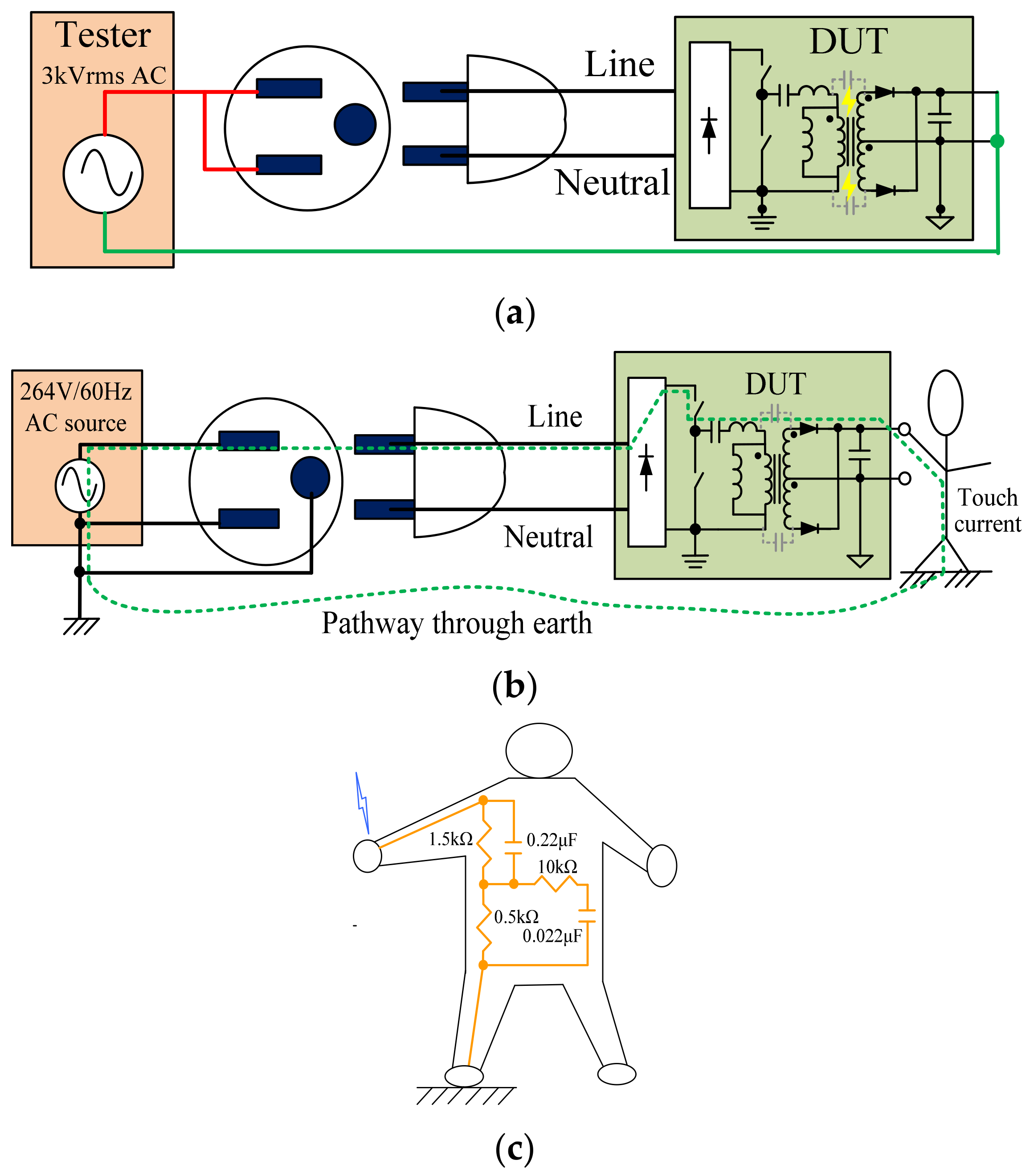
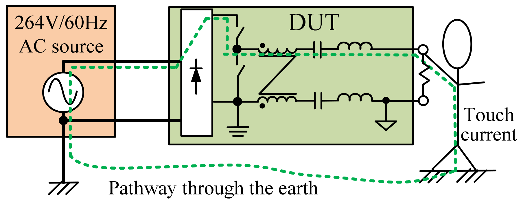
1.2. Test Methods and Requirements of Electrical Safety

For a commercial converter product, it is necessary to satisfy the requirements of the electrical safety test. There are two important certification items as shown in Figure 1: the dielectric strength test and touch current, which is also called the hipot test earth leakage current.
In the design process of a commercial converter product, it is important to satisfy the requirements of electrical safety. For example, for information and communication equipment products, the Underwriters Laboratories Inc. (UL), (Northbrook, IL, USA) and the International Electrotechnical Commission (IEC) define the standard documents of UL60950-1 [11] and IEC62368-1 [12], respectively. One of the requirements in these two standards is the dielectric strength test, commonly called a “dielectric withstand” or “hipot” test. The hipot test is a stress test of the insulation of a device under test (DUT).
As shown in Figure 1a, the hipot test applies a voltage that is much higher than the normal operating voltage to the DUT. For reinforced insulation products with a universal input voltage ranging from 85 Vac to 264 Vac, the required test voltages [11] may be 3000 Vac or equivalent to 4242 Vdc. When the equipment operates, the DUT is applied with a high voltage between the primary side and the secondary side or the earth ground to test its insulation breakdown status.
Table 2 and Figure 1b simply illustrate the touch current defined in the standards [11,12,13]. The touch current test simulates the effect of a person touching exposed metal parts of a product and detects whether or not the safe level of leakage current flows through the body to the earth. A high enough leakage current can cause an uncontrolled muscular spasm or shock. The equivalent circuit of the human body in [11,12,13] is defined in Figure 1c.
Converters used in data centers or communication centers are defined as grounded products, so the maximum touch current is 3.5 mA. The maximum touch current for an ungrounded (2 pin plug) product is 0.25 mA.
The creepage distance and clearance distance are also specified in the standard documents [11,12,14], as shown in Table 3. In offline converters used in homes or businesses, components such as PCBs, photo couplers, Y capacitors, transformers, etc., are required to comply with the electrical insulation system standards specified in safety regulations [11,12,14], and must have sufficient clearance distance and creepage distance, as shown in Table 3. In general, the primary-side winding to the secondary-side winding adopts double insulation or reinforced insulation, and the primary-side winding to the core adopts basic insulation. In order to reach a high insulation voltage, the insulation materials [15,16] and internal structure of a transformer are critical. The transformer contains many insulating materials, such as insulation tape [15], bobbins, margin spacers, and triple insulation wire [16], and so the transformer is bulky.

1.3. Prior Arts of Capacitive Insulation in Power Converters

As shown in Figure 2, a high-inductance common-mode choke in [17] works as a line-frequency low-pass filter to suppress touch current under the requirement limitations. However, the high-inductance common-mode choke on the DC output path usually induces lower conversion efficiency and higher cost. The experimental result of touch current is 0.734 mA. The hipot test is not discussed in [17]. In [18], there are two Y3 capacitors used as secondary-side switch zero voltage switching (ZVS) auxiliary components. Because the Y3 capacitors [19] cannot satisfy the requirement for reinforced or double insulation shown in Table 1, the main safety insulation and the energy transmission path are still via the transformer.
The traditional LLC converter is widely used because of its simple circuit structure and ZVS function. The basic structure is shown in Figure 3a. The resonance between the capacitor Cr, the resonant inductor Lr, and the transformer magnetizing inductance Lm can realize the ZVS of the switches Q1 and Q2, achieving high conversion efficiency. In many low-power applications, the leakage inductance Llk of the transformer is also used as the resonant inductor Lr. On the other hand, the resonant capacitor Cr generally adopts the plastic film capacitor, which is characterized by its high capacitance and low cost.
In the LLC converter presented in [20], the resonant capacitor Cr is replaced by the Y1 capacitor [21] to meet the clearance and creepage isolation requirements defined by the safety regulations. However, considering the design of EMI common mode noise, insulation current, and LLC voltage gain curve, the transformer is retained, but the transformer does not need to adhere to the electrical isolation requirements. The transformer as a whole can be regarded as a secondary component and only requires a basic insulation grade. Therefore, this transformer does not use triple insulated wire, and can use high-efficiency wires such as Litz wire and flat wires that are not reinforced insulation grades to minimize the insulation material in the transformer. Hence, the transformer structure and volume can be reduced so that a compact design of the magnetic component can be achieved.
In addition, since the rated withstand voltage of a typical triple insulated wire is only 3 kVac, applications requiring higher-voltage insulation such as power supplies for industrial equipment requiring 4.2 kVac [22] or auxiliary power supplies for solid state transformer systems with an insulation voltage of 25 kV [23] require expensive transformer insulation materials, resulting in more volume and cost. The proposed method only requires increasing the number of Y-capacitors in series to achieve higher insulation voltage without redesigning the transformer design.

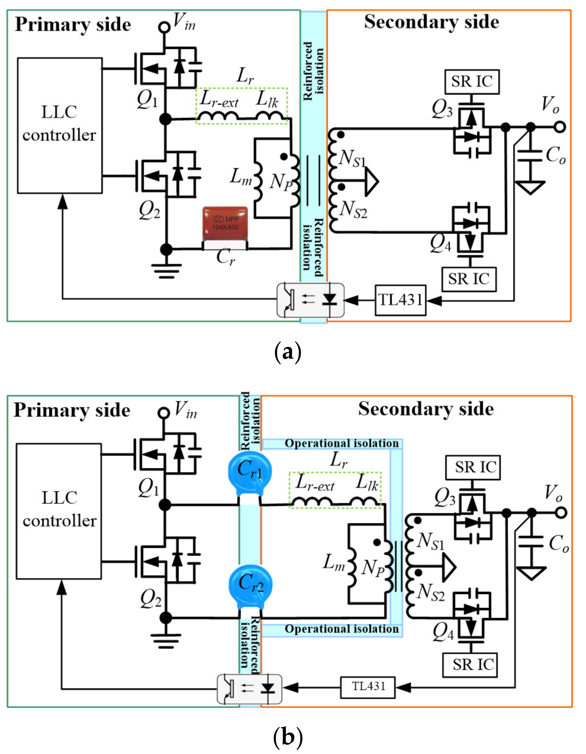
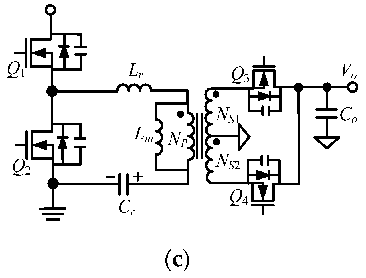
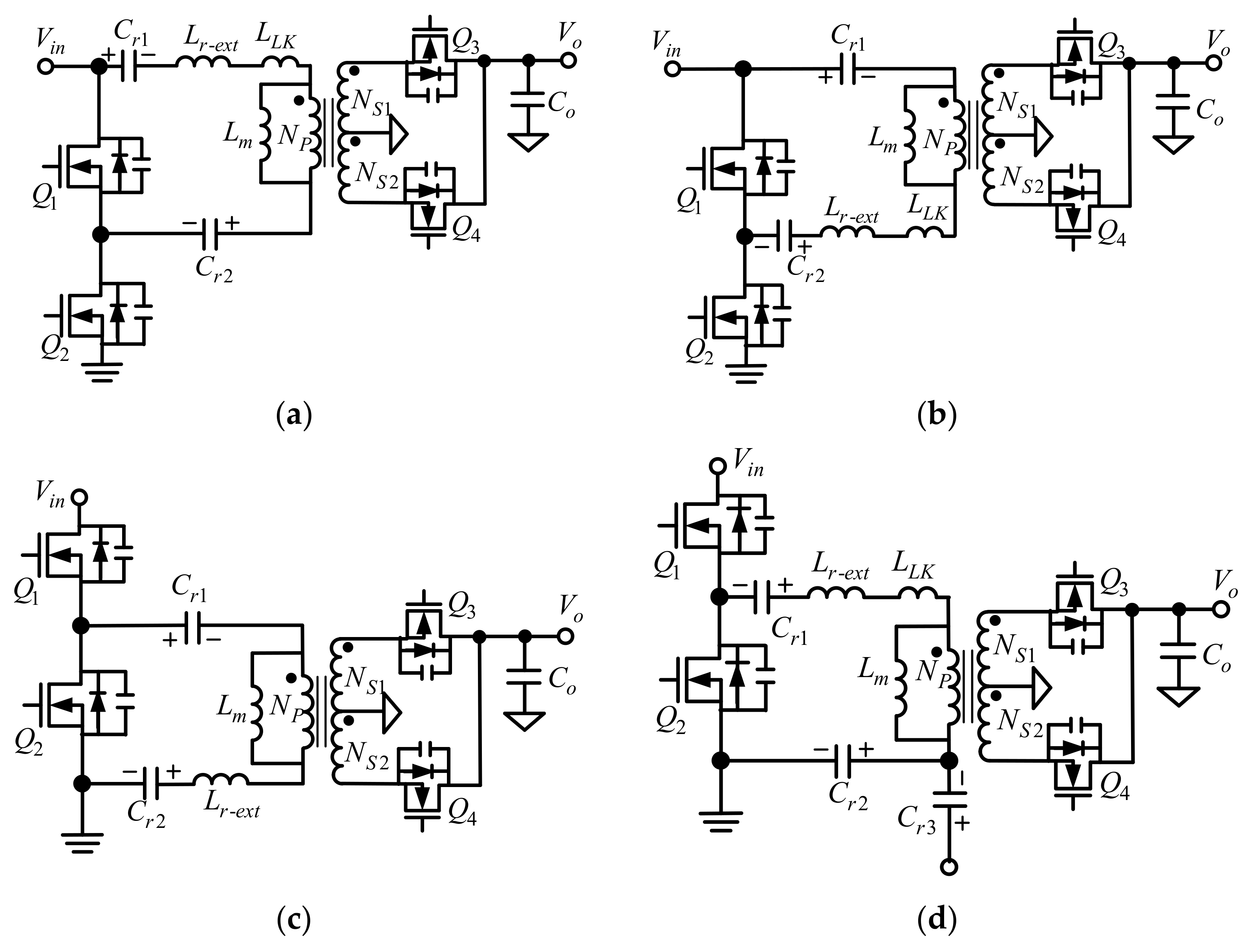
2. Proposed Circuit Configuration

Figure 3a shows the circuit structure of a typical LLC converter. The plastic film capacitor Cr works as a resonant capacitor, which is usually connected between the primary winding of the transformer and the primary side ground.
The proposed circuit is shown in Figure 3b. The single resonant capacitor is divided into two Y1 capacitors, named Cr1 and Cr2, so that safety regulations can be met. In the proposed LLC converter, the transformer plays a role in the functions of the resonant tank, voltage gain design, and common mode touch current blocker. The transformer is necessary for the reasons above. However, the volume and power density of the transformer are still improved via the reduction in transformer insulation materials.
Since the proposed method can keep the original transformer and minimize the insulation material in the transformer, the touch current is solved by isolation and the size is reduced. The circuits in Figure 3a,b have the same equivalent circuit shown in Figure 3c.
Compared with the method in [24], the mathematical theory of the proposed method is the same as the conventional LLC converter, so it can be driven by existing LLC control ICs and can be easily implemented for industrial applications.

3. Design Considerations

For design convenience, the components are chosen based on the traditional LLC converter and then the capacitor equivalent theorem to obtain Cr1 and Cr2. Table 4 shows the circuit specifications.

3.1. Design of Transformer T1

For the minimization of the LLC converter, the ferrite core LP22 with material JPP95 is chosen as T1, with a saturation flux density of 0.35 T at 120 °C according to the data sheet. Considering the component tolerance and the de-rating operation for mass production, the maximum flux density is designed to be 0.28 T. The minimum primary turns of T1 are designed as below:
N P ( min ) = V i n · D m a x 4 · B m a x · A e · f s w ( min ) = 25.3   Turns ,
For the convenience of production of the windings, the secondary turns are set as NS1 = NS2 = 2. It is suitable to design the turn ratio of T1 as an integer such that the value of NP is chosen as 28 turns to obtain a turn ratio of 14.

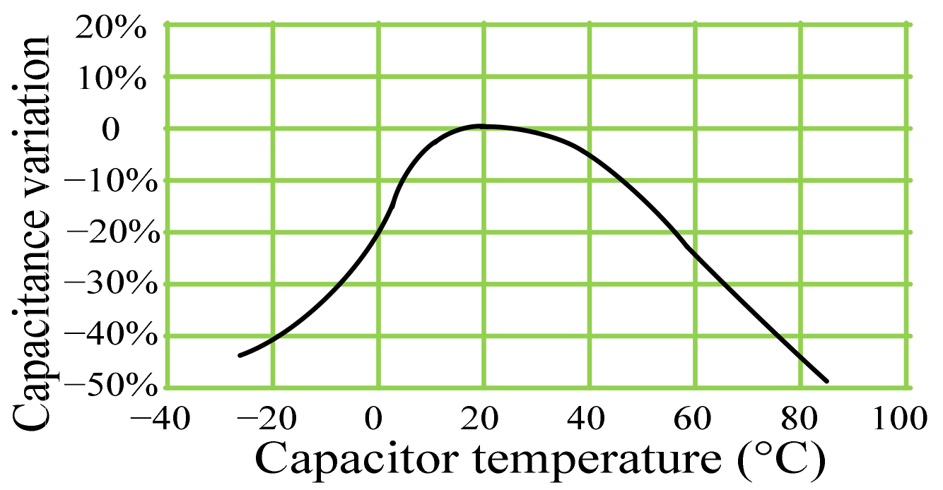
3.2. Design of Resonant Tank

By considering the unpredictable parasitic impedance caused by PCB traces, in practice, the voltage gain operating point at full load is usually set to be slightly lower than 1, generally 0.98. Based on NP = 28, the equivalent load impedance Rac-FL at full load and the equivalent load impedance Rac-LL at light load can be determined as follows:
R a c - F L = 8 · N P 2 π 2 · R o = 190.6   Ω ,
R a c - L L = 10 · 8 · N P 2 π 2 · R o = 1960.5   Ω ,
Compared to conventional LLC converters, which generally use a film capacitor as a resonant capacitor, the capacitance of the film capacitor has a low temperature coefficient of ±5%, so the capacitance can be considered a constant value when designing a conventional LLC converter. The proposed circuit uses Y1 capacitors for the resonant tank. Considering that the capacitance of the Z5U grade capacitor will change with the temperature, the higher the temperature is, the lower the capacitance. According to its data sheet [21], the capacitance variation curve is built in Figure 4 to establish that the capacitance of the 4.7 nF Y1 capacitor at a high temperature of 70 °C and 85 °C will decline by 35% and 50%, respectively, which is a critical point for designing the resonant tank.
The relationship between Cr1, Cr2 and Cr is as follows:
C r 1 = C r 2 = 2 C r ,
Since the maximum capacitance of the Y1 capacitor is 4.7 nF, considering the capacitance and volume, both Cr1 and Cr2 are designed as 9.4 nF (two 4.7 nF Y1 capacitors paralleled) in this prototype. Then, the value of Lr can be worked out as follows:
L r = 1 2 · π 2 · f r 2 · C r = 160   μ H ,
The value of Lm and the value of Llk are as follows:
L m = 4 · L r = 640   μ H ,   L l k = 17.6   μ H ,
Eventually, the resonance frequencies fs and fp, and the corresponding quality factors can be calculated as follows:
f s = 1 2 π L r · C r = 229.7   kHz ,
f p = 1 2 π ( L m + L r ) · C r = 102.7   kHz ,
Q F L = L r C r R a c - F L = 1.211 ,
Q L L = L r C r R a c - L L = 0.1211 ,

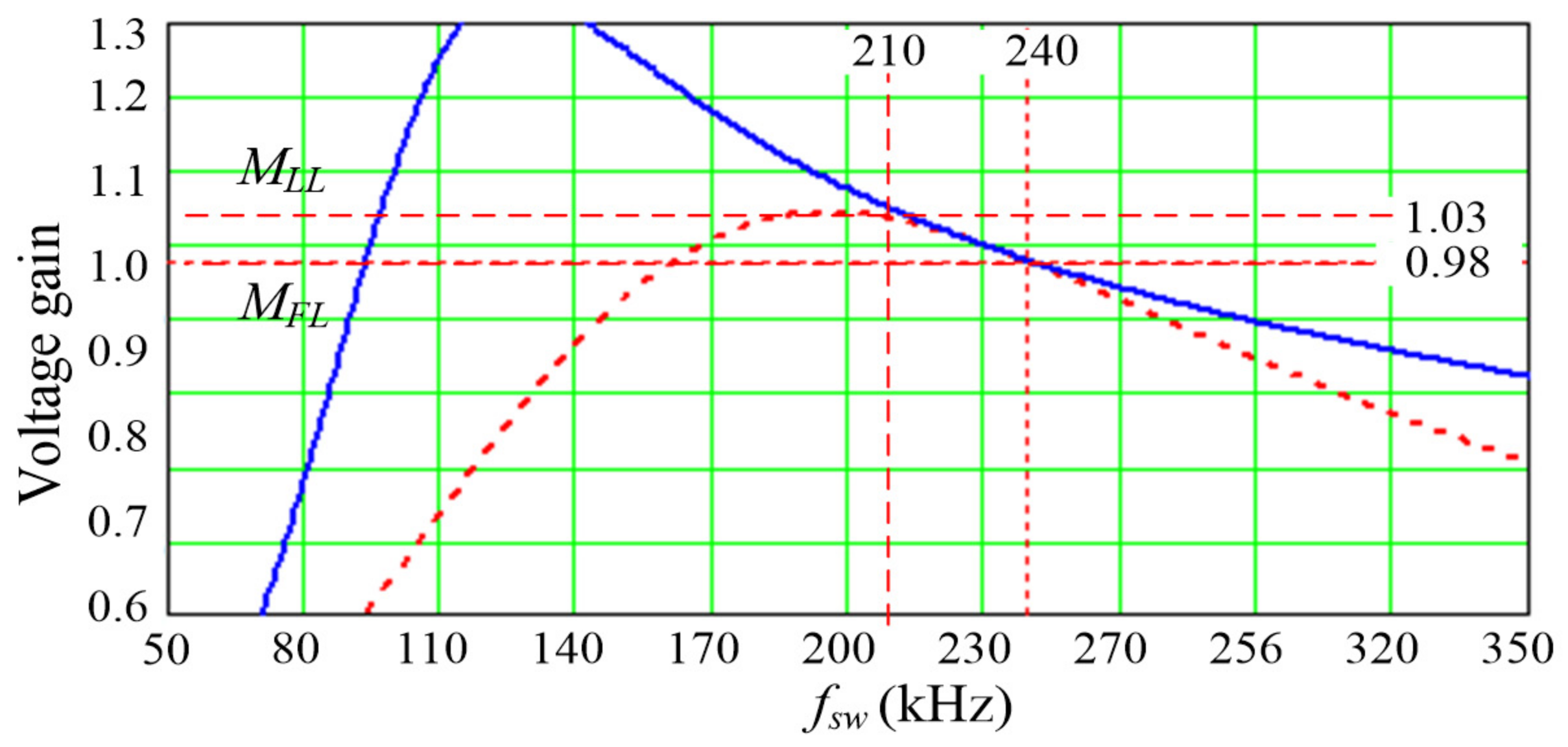
3.3. Voltage Gain for Light and Full Load

As shown in Figure 5, the voltage gain curves at 10% load and 100% load can be obtained. From this figure, it can be seen that the minimum Vin at 100% load is 380 V/1.03 = 369 V, corresponding to the circuit specifications shown in Table 2. In addition, the full-load voltage gain and the light-load voltage gain can be expressed as follows, where ω = 2πf:
M F L = ω 2 ω p 2 · k 1 + k i · ω ω s · 1 ω 2 ω s 2 · Q F L · k + 1 ω 2 ω p 2 ,
M L L = ω 2 ω p 2 · k 1 + k i · ω ω s · 1 ω 2 ω s 2 · Q L L · k + 1 ω 2 ω p 2 ,

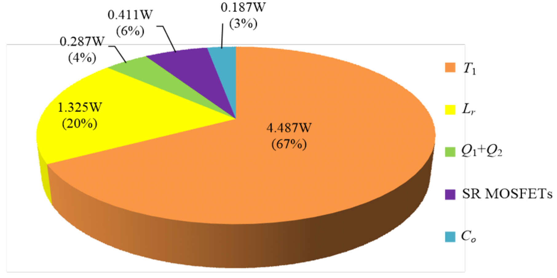
3.4. Loss Breakdown Analysis

The existing commercial 150 W LLC module from Asian Power Device Inc. (Taipei, Taiwan) is used as a reference in this paper. In order to make a fair comparison, the proposed prototype in this paper will adopt the same controller IC and MOSFETs as a reference. The proposed prototype only miniaturizes the magnetic component and replaces the resonant capacitor Cr using the film capacitor with high-side and low-side capacitors using Y1 capacitors. Due to the much lower capacitance of Y1 capacitors than that of film capacitors, the resonant tank parameter is redesigned to enhance the output power with higher switching frequency. The current of primary winding and the current of secondary winding can be calculated as follows:
i L ( pk ) = n · V o 4 · L m · f r = 0.285   A ,
i L r ( rms ) = V o 2 8 · n 2 · L m · f r 2 + π n · R o 2 = 0.819   A ,
i N s 1 ( rms ) = i N s 2 ( rms ) = I o · π 4 = 3.535   A ,
i C o ( rms ) = I o · π 2 2 2 I o 2 = 4.838   A ,
The magnetic flux of Lm also can be calculated as in (17).
B m a x - L m = L m · i L m ( pk ) N P · A e ( T 1 ) = 0.274   T ,
Based on the manufacturability of the T1, the NP is determined to be made with 28 turns of Litz wire with a diameter of 0.1 mm and 30 strands. NS1 and NS2 are both made with two turns of Litz wire with a diameter of 0.1 mm and 120 strands.
Eventually, the DC resistance of each winding is measured to be DCRNP = 9.2 mΩ and DCRNS1 = DCRNS2 = 164 μΩ so as to obtain the copper loss of T1, as shown in (18) and (19). The core loss of T1 is also obtained from (20) with core characteristics: Ve(T1) = 2480 mm3 and PCV(T1) = 1800 kW/m3.
P c o p p - N p = D C R N p i L r ( pk ) 2 2 = 6.16   mW ,
P c o p p - N s = D C R N s 1 i S R ( rms ) 2 + D C R N s 2 i S R ( rms ) 2 = 17   mW ,
P c o r e - T 1 = V e ( T 1 ) · P C V ( T 1 ) = 4.464   W ,
P T 1 = P c o p p - N p + P c o p p - N s + P c o r e - T 1 = 4.487   W ,
The voltage ratings of the resonant capacitors Cr1 and Cr2 are determined by (22) to (25):
v C r ( min ) = V i n n · V o I o · π 2 · n 2 i L m ( pk ) 2 C r L r = 65.4   V ,
v C r 1 ( min ) = v C r 2 ( min ) = 1 2 · v C r ( min ) = 32.7   V ,
v C r ( max ) = V i n v C r ( min ) = 452   V ,
v C r 1 ( max ) = v C r 2 ( max ) = 1 2 · v C r ( max ) = 226   V ,
The peak current and the RMS current of Lr-ext can be calculated as shown in (26) and (27):
i L r ( pk ) = i C r 1 ( pk ) = i C r 2 ( pk ) = V i n n · V o v C r ( min ) · L r C r = 1.158   A ,
i L r ( rms ) = i C r 1 ( rms ) = i C r 2 ( rms ) ,
In (5), it is known that Lr is 160 μH and Llk is 17.6 μH, and so the required value of Lr-ext should be 142.4 μH. Hence, an RM6 ferrite core is chosen with material JPP95 with the following key characteristics: Ae(Lr-ext) = 37.5 mm2 and Ve(Lr-ext) = 1090 mm3. Set Bmax-Lr = 0.28 T; then, the minimum number of turns required is calculated as follows:
N L r - e x t = L r - e x t · i L r ( pk ) B m a x · A e ( L r - e x t ) = 16.1   Turns ,
Based on the manufacturability of Lr-ext, NP is determined to be made with 30 turns of Litz wire with a diameter of 0.1 mm and 20 strands. Finally, the measured DC resistance of Lr-ext is DCRLr = 0.33 Ω to obtain the copper loss of Lr-ext, as shown in (29). The core loss of Lr-ext is also obtained as shown in (31) with the following core characteristics: Ae(Lr-ext) = 36.6 mm2, Ve(Lr-ext) = 1090 mm3, and PCV(Lr-ext) = 500 kW/m3:
P c o p p - L r - e x t = D C R L r i L r ( pk ) 2 2 = 0.235   W ,
B m a x - L r = L r - e x t · i L r ( pk ) N L r - e x t · A e ( L r - e x t ) = 0.15   T ,
P c o r e - L r - e x t = V e ( L r - e x t ) · P C V ( L r - e x t ) = 1.09   W ,
Finally, the total loss of Lr-ext is 1.325 W, as shown in (32):
P L r - e x t = P c o p p - L r - e x t + P c o r e - L r - e x t = 1.325   W ,
Here, we set the key parameters as Ron1 = Ron2 = 0.33 Ω, Qg1 = Qg2 = 13 nC, and vgs1 = vgs2 = 11 V for Q1 and Q2 to design the driving loss and conduction loss, which can be calculated as shown in (33) and (34). Due to the ZVS turn-on function of the LLC converter, the switching loss is unnecessary to consider:
P d r i v i n g ( Q 1 , Q 2 ) = 2 · Q g ( Q 1 , Q 2 ) · V g s ( Q 1 , Q 2 ) · f r = 66   mW ,
P c o n d ( Q 1 , Q 2 ) = 2 · R o n ( Q 1 , Q 2 ) · i L r ( rms ) 2 2 = 0.221   W ,
P Q 1 , Q 2 = P c o n d ( Q 1 , Q 2 ) + P d r i v i n g ( Q 1 , Q 2 ) = 0.287   W ,
Here, the key parameters, namely, Ron3 = Ron4 = 2.65 mΩ, Qg3 = Qg4 = 37 nC, and vgs3 = vgs4 = 8 V for Q3 and Q4, can be set to design the driving loss, and conduction loss can be determined as shown in (36) and (37). Due to the ZVS turn-on function of SR switches, the switching loss is unnecessary to consider. Two 470 μF/25 V solid capacitors are applied to the output capacitor Co. The data sheet provided by the manufacturer shows that the ESR of this capacitor is 16 mΩ and the corresponding ripple current capability is 4.65 A. Co needs to withstand the 4.83 A current ripple, as shown in (39). The combinational ESRCo is 8 mΩ. Therefore, the loss of the Co is shown in (40). Eventually, the total loss of the proposed LLC converter is shown in (41). Additionally, the estimated efficiency is 94.7%. The analysis of the loss breakdown is shown in Figure 6. The component list of the prototype is shown in Table 5.
P d r i v i n g ( S R ) = 2 · Q g ( S R ) · V g s ( S R ) · f r = 0.136   W ,
P c o n d ( S R ) = 2 · R o n ( S R ) · i S R ( rms ) 2 = 0.275   W ,
P S R = P c o n d ( S R ) + P d r i v i n g ( S R ) = 0.411   W ,
i C o ( rms ) = i S R ( rms ) 2 I o 2 = 4.83   A
P C o = i C o ( rms ) 2 · E S R C o = 0.187   W
P t o t a l = P T 1 + P L r - e x t + P Q 1 , Q 2 + P S R + P C o = 6.697   W

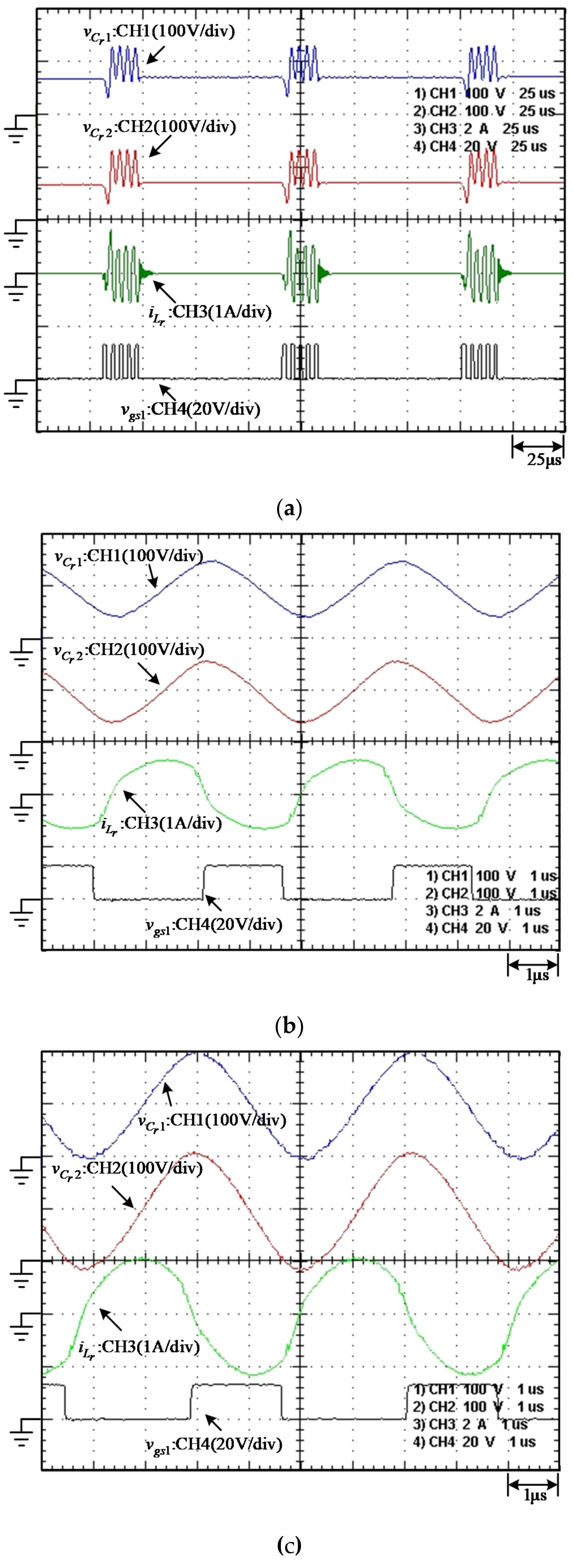
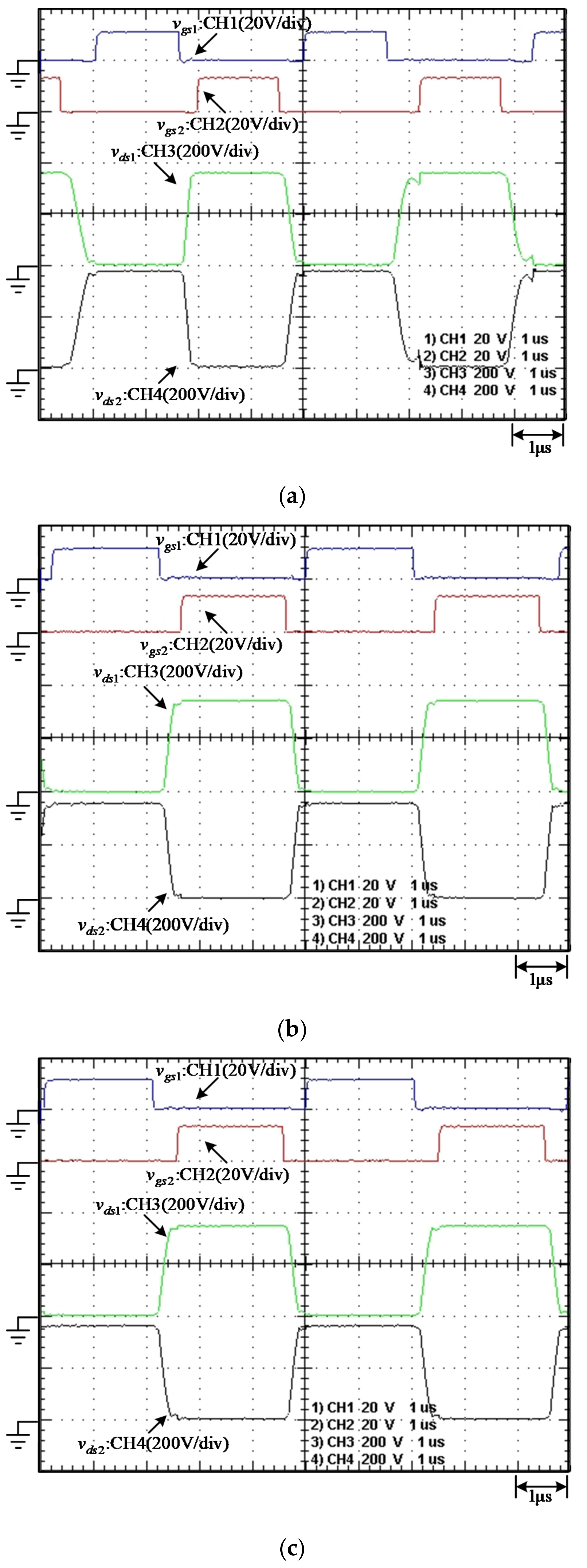
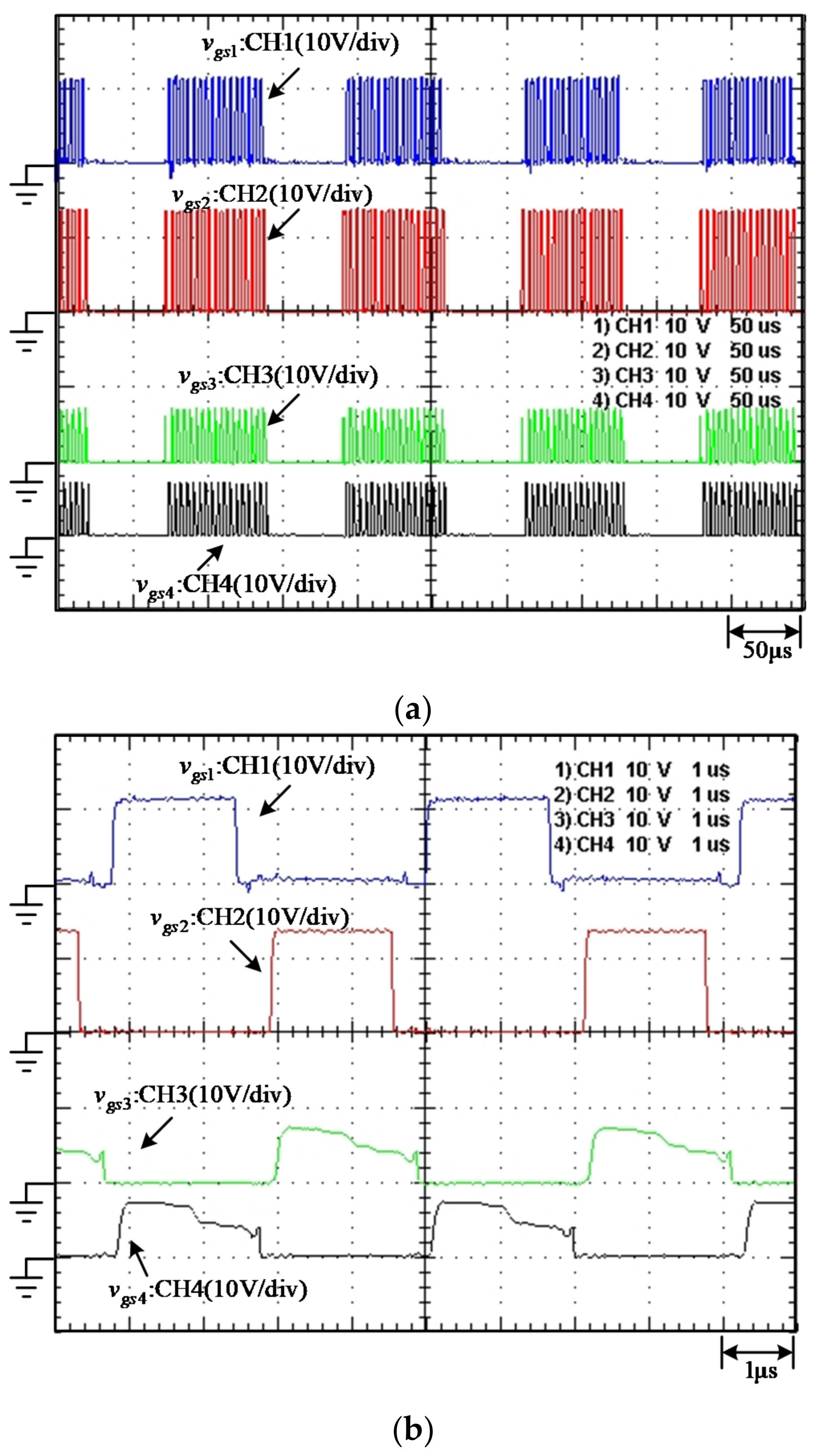
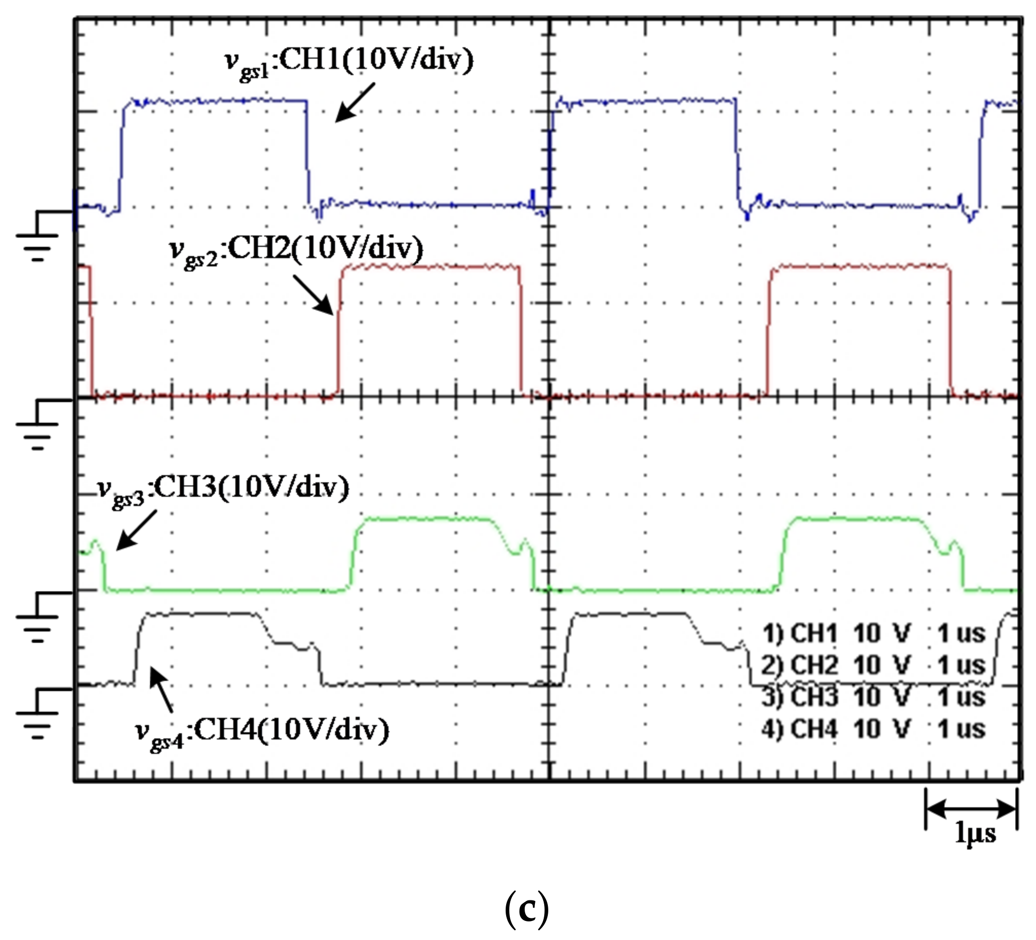
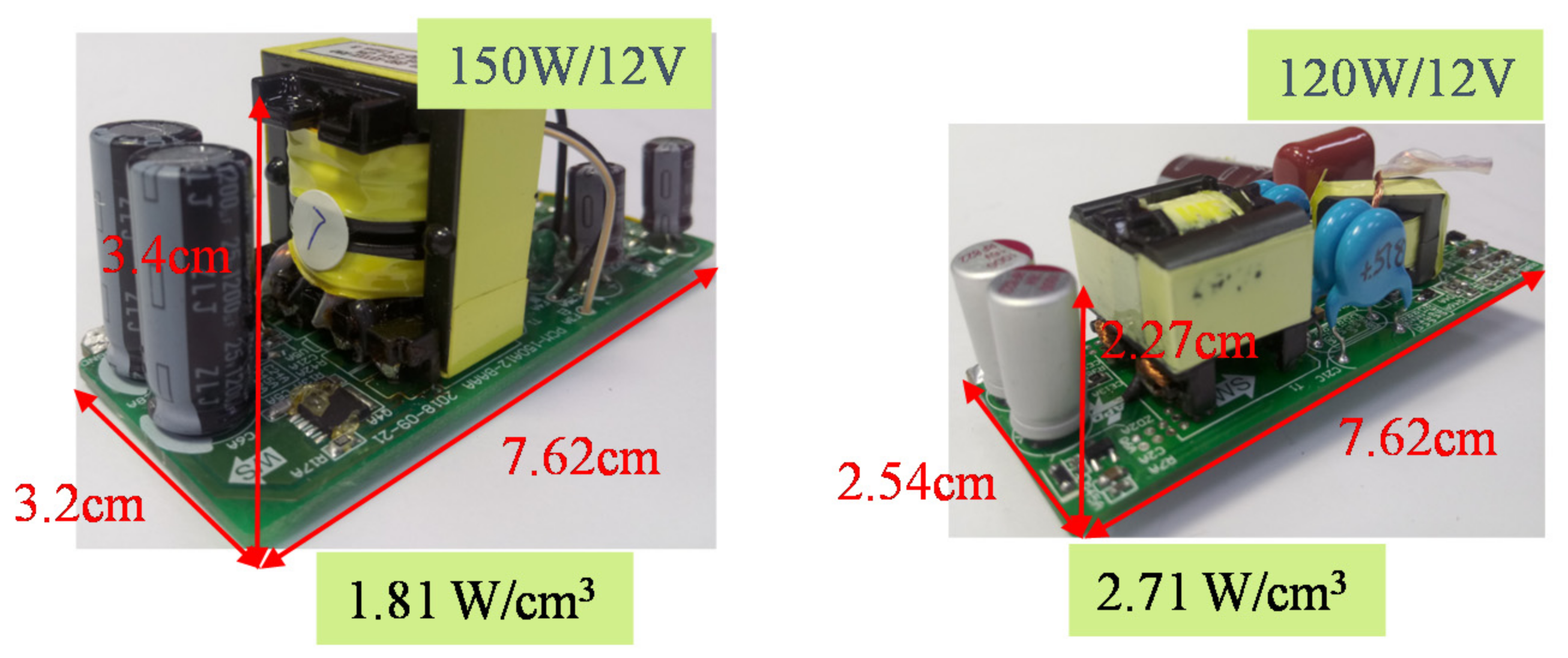
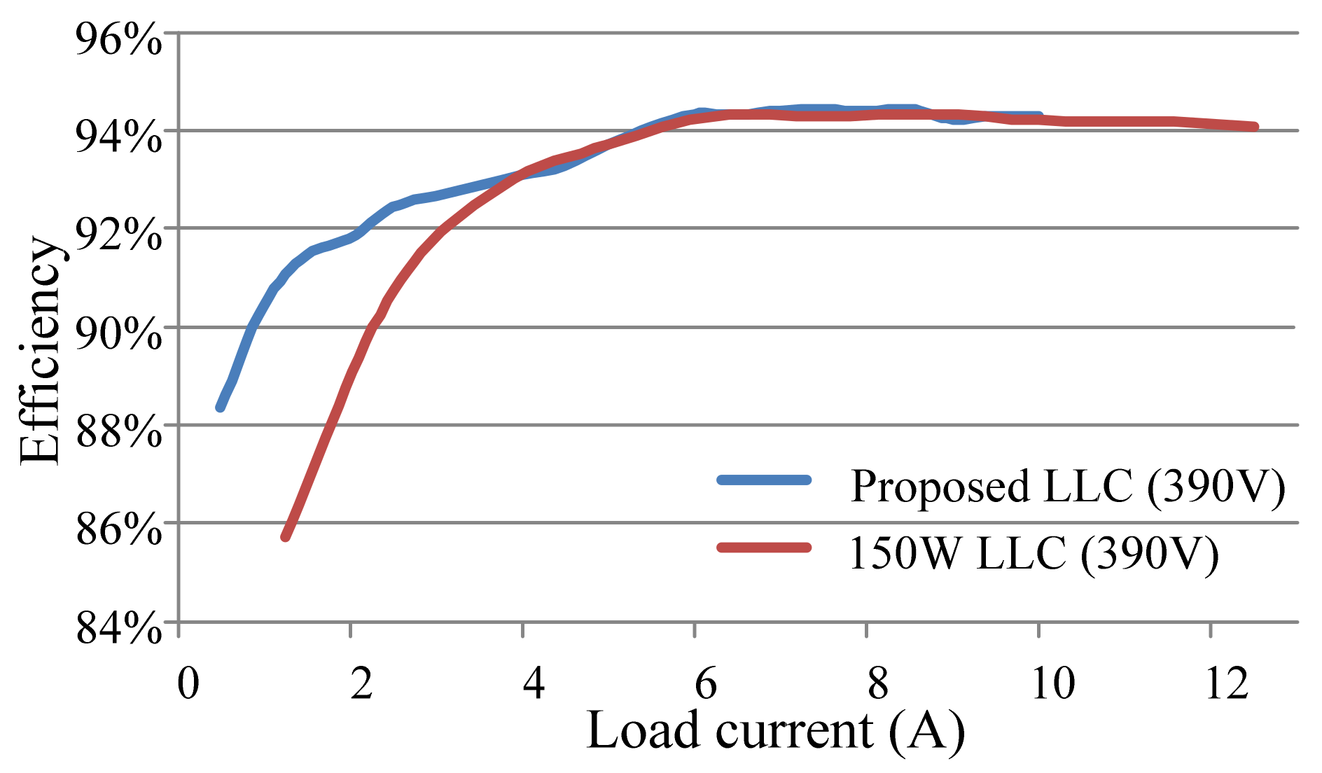
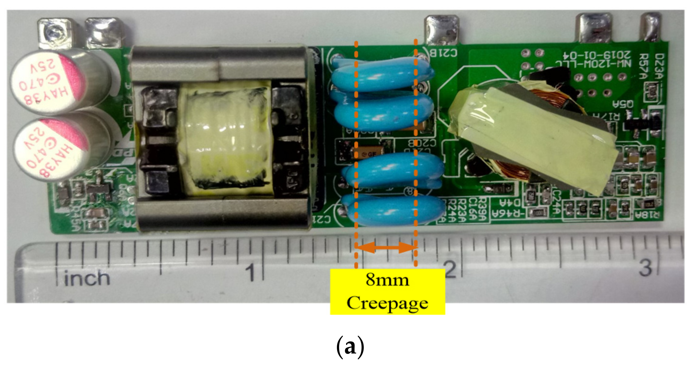
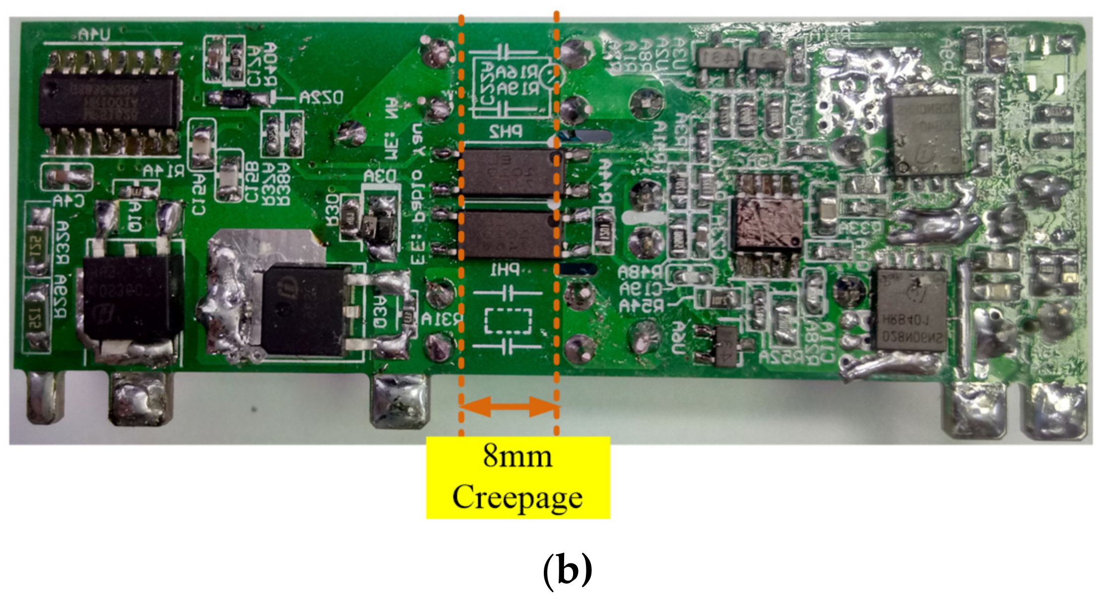
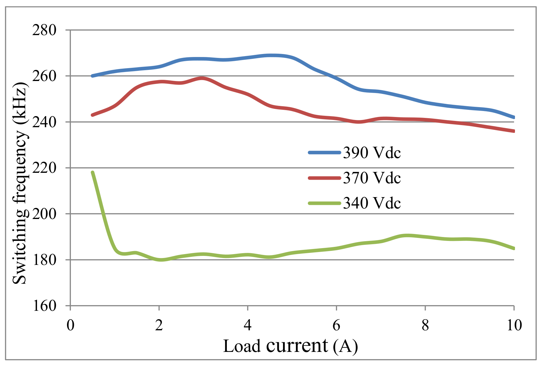
4. Experimental Results

The traditional circuit shown in Figure 7a and the proposed circuit shown in Figure 7b adopt individual Y1 capacitors, named CY, to remove common-mode EMI without affecting circuit behavior. These two have the same input voltage, output voltage, primary-side LLC controller IC, secondary-side SR controller IC, and MOSFETs, except for resonant parameters and transformer parameters.
Figure 8a–c present the measured waveforms of vcr1, vcr2, iLr, and vgs2 at 10%, 50%, and 100% load, respectively. It can be seen that when the load is lower than 40%, the converter enters burst mode operation, which is a common technology that improves the efficiency of the LLC at a light load for the commercial LLC IC in industry applications. As the load current increases, the amplitudes of vCr1, vCr2, and iLr will increase. It can be observed that the operation of the burst mode allows the light-load frequency to be reduced to maintain a relatively high iLr, so that the resonant tank has enough energy for the output capacitance Coss of the MOSFET to be charged and discharged, as well as to obtain near-ZVS. As the load increases, iLr increases, and complete ZVS can be achieved. Figure 9a–c show the measured waveforms of vgs1, vgs2, vds1, and vds2 at 10%, 50, and 100% load, respectively. Both switches are near-ZVS or ZVS.
Figure 10a–c display the measured waveforms of vgs1, vgs2, vgs3, and vgs4 at 10%, 50%, and 100% load, respectively. All the switches operate as the traditional LLC converter. The reduction in the voltages on vgs3 and vgs4 is a patented driving mechanism [25]. This mechanism can keep vds3 and vds4 at around −40 mV, even when the current through the MOSFET is low. This function puts the gate driving voltage at a low level when the synchronous MOSFET is turned off, which shortens the turn-off time. When vds3 or vds4 rises to trigger the turn-off threshold of +40 mV, the gate driving voltage drops to zero rapidly.
All the measured efficiency results do not include the front-end bridge rectifier and power factor correction stage. From Figure 11, it can be observed that the efficiency throughout the load range is above 87.5% and can be up to 95%. Even though the prototype is designed with a specification of DC input voltage from 370 V to 390 V, the final prototype can still work with lower input voltage down to 340 V DC and perform similar conversion efficiency, which is helpful to extend the hold-up time further.
The proposed prototype is compared with the 150 W LLC DC-DC module product from Asian Power Device Inc. (Taipei, Taiwan). Their LLC controller, primary-side switches, and SR switches are all the same.
As shown as Figure 12, the former LLC DC-DC module is a 150 W product from Asian Power Device Inc. with a power density of 1.81 W/cm3, and the latter is a 120 W product with a power density of 2.71 W/cm3. The proposed prototype has a higher power density than the traditional circuit due to the reduction in the size of the transformer.
The efficiency comparison is shown in Figure 13. The proposed prototype has the same efficiency performance when the load current is above 4 A. The prototype has higher efficiency under light load conditions due to the burst mode setting point at 40% load.
The experimental setup of the safety test method is shown in Figure 1 and Figure 7. The front-end bridge rectifier and the power factor correction stage are included during the safety test. Finally, the leakage current of the proposed circuit with 3 kV/60 Hz hipot test conditions is 80 μA. The leakage current test is operated with a working DUT with an input voltage of 264 V/60 Hz and full load conditions. The experimental leakage current of the proposed circuit is only 10 μA, which is far below the limitation of 0.5 mA.
Figure 14a,b show the photos from the top view and bottom view, respectively. The resonant capacitors Cr1 and Cr2 provide 8 mm creepage to meet the reinforced insulation requirements [13,14,26]. The two photo couplers work as signal isolators on the feedback path.
The resonant capacitors used in this paper are ceramic capacitors, which generally have a high temperature coefficient, so the capacitance value is affected by component temperature, and this should be taken into consideration in the circuit design. Figure 15a,b correspondingly show the thermography photos from the top view and bottom view under full load operation and natural convection, respectively. As shown as Figure 15, the actual operation of Cr1 and Cr2 is around 56 °C to obtain capacitance variation of −20%. The hotpot is at the SR control IC, which is located too close to the heat sources of T1, Q3, and Q4.
In a conventional LLC converter design, the switching frequency decreases as the output load increases, and the switching frequency shifts to region II to increase the voltage gain. The higher the output power, the higher the thermal radiation from Lr and T1, the higher the temperature of Cr1 and Cr2, the lower the capacitance of Cr1 and Cr2, and the higher the fs will rise, causing the fsw to move to region II. When the rate of increase in fs due to the decrease in capacitance is equal to the decrease in fsw due to the increase in the output load, it can be observed that the fsw decreases insignificantly after the half load of the proposed circuit, as shown in Figure 16.
In terms of circuit design, the temperature of the components can be obtained from the heat flow simulations by the mechanical engineer, and then the temperature change curve provided by the data sheet can be used to estimate the change in capacitance caused by the temperature. In addition, during the period of the PCB layout, the capacitor should be placed upwind of the cooling air flow to avoid being close to heat-generating components such as switch devices or magnetic components to reduce the temperature rise.
If a more stable capacitance value is required, the X7R grade capacitor [27,28] is recommended, with a capacitance variation of less than 15% and 20% over the temperature range of −55 °C to +125 °C, respectively.
Table 6 shows the comparison between the proposed and the existing methods. It can be found that the proposed method can satisfy the safety requirement of the IEC60950-1 standard and achieve higher conversion efficiency and power density.
Figure 17 shows the four possible derivative circuits of the proposed circuit in this research. Because they all have the same operating principles, they are considered to have high feasibility.

5. Conclusions

In this paper, the resonant capacitor is cut into two resonant capacitors, which are used to share the isolation capacity of the transformer. The benefits of the proposed method are as follows. First, the creepage of the transformer is effectively transferred to the Y1 capacitor by the proposed method. The volume of the transformer is significantly reduced. The proposed converter has a higher power density than the traditional converter. The proposed prototype with 120 W was briefly compared with the traditional prototype with 150 W to verify the feasibility of the proposed isolated structure. Second, the rated insulation voltage of a normal three-layer insulated wire is only 3 kVac. However, some applications require higher insulation voltage, such as power supplies for industrial equipment or the auxiliary power supplies for solid state transformer systems, where the insulation voltage required is up to 25 kV. The proposed approach only requires an increase in the number of Y-capacitors in series to achieve a higher insulation voltage without modifying the transformer design.

Author Contributions

Conceptualization, Y.-T.Y.; methodology, Y.-T.Y.; software, Y.-T.Y.; validation, T.-L.H.; formal analysis, Y.-T.Y.; investigation, T.-L.H.; resources, T.-L.H.; data curation, T.-L.H.; writing—original draft preparation, Y.-T.Y.; writing—review and editing, Y.-T.Y.; visualization, Y.-T.Y.; supervision, Y.-T.Y.; project administration, Y.-T.Y.; funding acquisition, T.-L.H. All authors have read and agreed to the published version of the manuscript.

Funding

This research was supported by the Ministry of Science and Technology, Taiwan, under the Grant Number: MOST 109-2222-E-167-003-MY3.

Institutional Review Board Statement

Not applicable.

Informed Consent Statement

Not applicable.

Data Availability Statement

No new data were created or analyzed in this study. Data sharing is not applicable to this article.

Conflicts of Interest

The authors declare no conflict of interest.

Abbreviations

Q1, Q2Main switches
Q3, Q4SR switches
CoOutput capacitor
T1Main transformer
NPPrimary winding of T1
NS1, NS2Secondary windings of T1
nTurn ration of T1
LrResonance inductor
LlkLeakage inductance of Np of T1
Lr-extAdditional resonance inductor
CrResonant capacitor
Cr1High-side resonant capacitor
Cr2Low-side resonant capacitor
DmaxMaxima duty cycle
BmaxMaxima flux density of T1
fpResonant frequency of Lr, Lm, and Cr
fsResonant frequency of Lr and Cr
fswSwitching frequency (Hz)
QFL, QLLQuality factor of full load and light load, respectively
RoEquivalent resistance of output load
Rac-FL, Rac-LLReflected load resistance of output load at full load and light load, respectively
ωSwitching frequency (rad/sec)
ωpResonance frequency of parallel resonant converter
ωsResonance frequency of series resonant converter
MFL, MLLVoltage gain of the output and input at full load and light load, respectively
AeEffective core area
vCrVoltage cross Cr
vCr(min)Minima voltage of Cr
vCr(max)Maxima voltage of Cr
iCr1(pk)Peak current of Cr1
vCr1Voltage cross Cr1
vCr1(min)Minima voltage of Cr1
vCr1(max)Maxima voltage of Cr1
iCr2(pk)Peak current of Cr2
vCr2Voltage cross Cr2
vCr2(min)Minima voltage of Cr2
vCr2(max)Maxima voltage of Cr2
Np(min)Minima required turns of Np
iNp(rms)RMS current of Np
iNs1(rms), iNs2(rms)RMS current of Ns1 and Ns2, respectively
Bmax-LmMaxima flux density of Lm
iLm(pk)Peak current of Lm
DCRNpDCRNp resistance of Np
DCRNs1, DCRNs2DCRNp resistance of Ns1 and Ns2
Ae(T1)Effective core area of T1
Ve(T1)Effective core volume of T1
Pcopp-NpCopper loss of Np
Pcopp-NsCopper loss of Ns
Pcore-T1Core loss of T1
PCV(T1)Unit core loss of T1
PT1Total loss of T1
iLr(pk)Peak current of Lr
NLr-extWinding turns of Lr-ext
Lr-extAdditional resonant inductor
Ae(Lr-ext)Effective core area of Lr-ext
Bmax-LrMaxima flux density of Lr-ext
Ve(Lr-ext)Effective core volume of Lr-ext
PCV(Lr-ext)Core loss of unit volume of Lr-ext
DCRLrDC resistance of Lr-ext
iLr(rms)RMS current of Lr-ext
Pcore-Lr-extCore loss of Lr-ext
Pcopp-Lr-extCopper loss of Lr-ext
PLr-extTotal loss of Lr-ext
Ron(Q1,Q2)Conduction resistance of Q1 and Q2
Pcond(Q1,Q2)Conduction loss of Q1 and Q2
Vgs(Q1,Q2)Maxima driving voltage of Q1 and Q2
Qg(Q1,Q2)Gate charge of Q1 and Q2
Pdriving(Q1,Q2)Driving loss of Q1 and Q2
PQ1,Q2Total loss of Q1 and Q2
Ron(SR)Conduction resistance of Q3 and Q4
iSR(rms)RMS current of Q3 and Q4
Pcond(SR)Conduction loss of Q3 and Q4
Qg(SR)Gate charge of Q3 and Q4
Vgs(SR)Maximum driving voltage of Q3 and Q4
Pdriving(SR)Driving loss of Q3 and Q4
Pcond(SR)Conduction loss of Q3 and Q4
PSRTotal loss of Q3 and Q4
iCo(rms)RMS ripple current of Co at low line and high line Vin
ESRCoEquivalent series resistance of Co
PCoTotal loss of Co
PtotalTotal loss of system

References

  1. UL60384-14; Fixed Capacitors for Use in Electronic Equipment—Part 14: Sectional Specification: Fixed Capacitors for Electromagnetic Interference Suppression and Connection to the Supply Mains. UL Standard: Northbrook, IL, USA, 2013.
  2. Bazarov, A.; Abramovitz, A.; Shmilovitz, D. Multi-string capacitively isolated quasi-resonant LED driver. In Proceedings of the Conference Record of the IEEE International Aegean Conference on Electrical Machines and Power Electronics & International Conference on Optimization of Electrical and Electronic Equipment (OPTIM & ACEMP), Istanbul, Turkey, 8–10 September 2011; pp. 711–716. [Google Scholar]
  3. Kline, M.; Izyumin, I.; Boser, B.; Sanders, S. A transformerless galvanically isolated switched capacitor LED driver. In Proceedings of the Conference Record of the IEEE Applied Power Electronics Conference and Exposition (APEC), Orlando, FL, USA, 5–9 February 2012; pp. 2357–2360. [Google Scholar]
  4. Dos Santos Filho, E.E.; Miranda, P.H.A.; Sa, E.M.; Antunes, F.L.M. A LED driver with switched capacitor. IEEE Trans. Ind. Appl. 2014, 50, 3046–3054. [Google Scholar] [CrossRef]
  5. Zhang, J.; Wang, J.; Wu, X. A capacitor-isolated LED driver with inherent current balance capability. IEEE Trans. Ind. Electron. 2012, 59, 1708–1716. [Google Scholar] [CrossRef]
  6. Eloi, E.; Sá, E.M., Jr.; dos Santos, R.L.; Miranda, P.A.; Antunes, F.L. Single stage switched capacitor LED driver with high power factor and reduced current ripple. In Proceedings of the Conference Record of the IEEE Applied Power Electronics Conference and Exposition (APEC), Charlotte, NC, USA, 15–19 March 2015; pp. 906–912. [Google Scholar]
  7. Shmilovitz, D.; Abramovitz, A.; Reichman, I. A family of bridgeless quasi-resonant LED drivers. IEEE Trans. Power Electron. 2016, 31, 1833–1836. [Google Scholar] [CrossRef] [Green Version]
  8. Kline, M.; Izyumin, I.; Boser, B.; Sanders, S. Capacitive power transfer for contactless charging. In Proceedings of the Conference Record of the IEEE Applied Power Electronics Conference and Exposition (APEC), Fort Worth, TX, USA, 6–10 March 2011; pp. 1398–1404. [Google Scholar]
  9. Musavi, F.; Edington, M.; Eberle, W. Wireless power transfer a survey of EV battery charging technologies. In Proceedings of the Conference Record of the IEEE Energy Conversion Congress and Exposition (ECCE), Raleigh, NC, USA, 15–20 September 2012; pp. 1804–1810. [Google Scholar]
  10. Rozario, D.; Azeez, N.A.; Williamson, S.S. Comprehensive review and comparative analysis of compensation networks for capacitive power transfer systems. In Proceedings of the Conference Record of the IEEE International Symposium on Industrial Electronics (ISIE), Santa Clara, CA, USA, 8–10 June 2016; pp. 823–829. [Google Scholar]
  11. UL 60950-1; Information Technology Equipment-Safety—Part 1: General Requirements. UL Standard: Northbrook, IL, USA, 2007.
  12. IEC 62368-1; Audio-Video, Information and Communication Technology Equipment. IEC Standard: Geneva, Switzerland, 2018.
  13. IEC60990; Methods of Measurement of Touch Current and Protective Conductor Current. UL Standard: Northbrook, IL, USA, 2016.
  14. UL 840; Insulation Coordination Including Clearances and Creepage Distances for Electrical Equipment. UL Standard: Northbrook, IL, USA, 2005.
  15. Datasheet of 3M Polyester Film Electrical Tape 1351-1 with Acrylic Adhesive. Available online: https://multimedia.3m.com/mws/media/86183O/3m-polyester-film-electrical-tape-1351-1-data-sheet-78-8125-9439-4-b.pdf (accessed on 1 April 2021).
  16. UL 2353; Single- and Multi-Layer Insulated Winding Wire. UL Standard: Northbrook, IL, USA, 2016.
  17. Zhu, J.; Xu, M.; Sun, J.; Wang, C. Novel capacitor-isolated power converter. In Proceedings of the Conference Record of the IEEE Energy Conversion Congress and Exposition (ECCE), Atlanta, GA, USA, 12–16 September 2010; pp. 1824–1829. [Google Scholar]
  18. Lim, S.; Hanson, A.J.; Santiago-González, J.A.; Perreault, D.J. Capacitively aided switching technique for high-frequency isolated bus converters. In Proceedings of the Conference Record of the IEEE Applied Power Electronics Conference and Exposition (APEC), Long Beach, CA, USA, 20–24 March 2016; pp. 98–105. [Google Scholar]
  19. Application Note of Safety Considerations in Power Supply Design. Available online: https://www.ti.com/seclit/ml/slup227/slup227.pdf (accessed on 1 January 2005).
  20. Yau, Y.T.; Hung, T.-L.; Hwu, K.I. A capacitive isolated LLC converter. In Proceedings of the Conference Record of the IEEE Applied Power Electronics Conference and Exposition (APEC), Online, 14–17 June 2021. [Google Scholar]
  21. Reliability Test Data of DE1E3KX472M. Available online: https://search.murata.co.jp/Ceramy/image/img/A01X/RTD-E0440EB_DE1E3KX472M%5E%5E%5EN01F.pdf (accessed on 1 January 2005).
  22. MKE15-HI Datasheet. Available online: www.minmax.com.tw/en/download/files/1718/MKE15-HI_Datasheet.pdf (accessed on 3 September 2020).
  23. Liu, J.; Zhong, S.; Zhang, J.; Ai, Y.; Zhao, N.; Yang, J. Auxiliary power supply for medium-/high-voltage and high-power solid-state transformers. IEEE Trans. Power Electron. 2020, 35, 4791–4803. [Google Scholar] [CrossRef]
  24. Kehler, L.B.; Kaminski, A.M.; Pinheiro, J.R.; Rech, C.; Marchesan, T.B.; Emmel, R.R. Auxiliary power supply for solid state transformers. In Proceedings of the Conference Record of the IEEE International Conference on Electronics Circuits and Systems (ICECS), Monte Carlo, Monaco, 11–14 December 2016; pp. 193–196. [Google Scholar]
  25. MP6924 Datasheet. Available online: https://www.monolithicpower.com/en/documentview/productdocument/index/version/2/document_type/Datasheet/lang/en/sku/MP6924GS-Z/document_id/4899/ (accessed on 15 September 2017).
  26. GB 4943. 1-2011; Information Technology Equipment-Safety—Part 1: General Requirements. National Standard of the People’s Republic of China: Beijing, China, 2011.
  27. Datasheet of Ceramic Chip Safety Capacitors Class X and Y. Available online: https://www.kekon.com/pdf/ceramichipsafety.pdf (accessed on 1 January 2005).
  28. Datasheet of Type RB Safety Standard Certified Lead Type Disc Ceramic Capacitors for General Purpose. Available online: https://search.murata.co.jp/Ceramy/image/img/A01X/G101/ENG/DE1_RB_R01F_E.pdf (accessed on 1 January 2005).
Figure 1. Electrical safety test: (a) hipot, (b) touch current, (c) human body model.
Applsci 12 04950 g001
Figure 2. Conventional capacitor isolation converter.
Applsci 12 04950 g002
Figure 3. Circuit structures: (a) traditional LLC converter, (b) proposed architecture, (c) simplified architecture of (a,b).
Applsci 12 04950 g003aApplsci 12 04950 g003b
Figure 4. Capacitance change curve of Cr1 and Cr2.
Applsci 12 04950 g004
Figure 5. Voltage gain curves at 10% load and 100% load.
Applsci 12 04950 g005
Figure 6. Loss breakdown analysis.
Applsci 12 04950 g006
Figure 7. Actual circuit structure: (a) traditional; (b) proposed.
Applsci 12 04950 g007
Figure 8. Measured waveforms: vcr1, vcr2, iLr, and vgs2 under (a) 10% load, (b) 50% load, and (c) 100% load.
Applsci 12 04950 g008
Figure 9. Measured waveforms: vgs1, vgs2, vds1, and vds2 under (a) 10% load, (b) 50% load, and (c) 100% load.
Applsci 12 04950 g009
Figure 10. Measured waveforms: vgs1, vgs2, vgs3, and vgs4 under (a) 10% load, (b) 50% load, and (c) 100% load.
Applsci 12 04950 g010aApplsci 12 04950 g010b
Figure 11. Curves of efficiency versus load current.
Applsci 12 04950 g011
Figure 12. Power density comparison.
Applsci 12 04950 g012
Figure 13. Curves of efficiency versus load current for proposed LLC and 150 W LLC.
Applsci 12 04950 g013
Figure 14. Photos of the proposed prototype: (a) top view, (b) bottom view.
Applsci 12 04950 g014aApplsci 12 04950 g014b
Figure 15. Thermography photos of the proposed prototype: (a) top view, (b) bottom view.
Applsci 12 04950 g015
Figure 16. Measured curves of switching frequency.
Applsci 12 04950 g016
Figure 17. Derivation of the proposed circuit structure: (a) Type 1, (b) Type 2, (c) Type 3, (d) Type 4.
Applsci 12 04950 g017
Table 1. Classification of class Y capacitors.
SubclassType of Insulation BridgedRange of Rated VoltagesPeak Impulse Voltage before Endurance Test
Y1Double insulation or reinforced insulation≤500 V8.0 kV
Y2Basic insulation or supplementary insulation≥150 V
≤300 V
5.0 kV
Y3Basic insulation or supplementary insulation≥150 V
≤250 V
None
Y4Basic insulation or supplementary insulation≤150 V2.5 kV
Table 2. Limitation of touch current.
Type of EquipmentMaximum Touch Current
Information equipment without earth ground connection0.25 mA
Hand-held information equipment with earth ground connection0.75 mA
Stationary, pluggable information equipment with earth ground connection3.5 mA
Table 3. Creepage distance and clearance distance.
Insulation LevelCreepage DistanceClearance Distance
Basic or supplementary insulation3.2 mm2.0 mm
Double or reinforced insulation6.4 mm4.0 mm
Table 4. Circuit specifications.
ParameterSpecification
Rated input voltage (Vin)370 V~390 V
Rated output voltage (Vo)12 V
Rated output current (Io)10 A
Resonant frequency (fs)230 kHz
Minimum switching frequency (fsw(min))210 kHz
Magnetizing inductance divided by resonant inductance (k)4
Maxima duty cycle (Dmax)0.42
Estimated efficiency (η)96%
Table 5. Component specifications.
SymbolsDescription
Cr1, Cr24.7 nF//4.7 nF, DE1E3KX472M, Murata, Kyoto, Japan, 300 Vac Class Y1 Reinforced Insulation Capacitors with IEC384-14 Safety Recognized
Lr-extRM6, 142.4 μH, JPP95, A-core Inc., Jiangmen, China
T1LP22, 640 μH, 28:2:2, JPP95, A-core Inc., Jiangmen, China
Q1, Q2IPD60R360P7S, DPAK, Infineon AG, Warstein, Germany
Q3, Q4BSC028N06NS, TDSON8, Infineon AG, Warstein, Germany
Co470 μF//470 μF; Conductive Polymer Aluminum Cap, APAQ Co., Maioli, Taiwan
LLC Controller ICHR1001A, Monolithic Power Systems Inc., Kirkland, WA, USA
SR Controller ICMP6924, Monolithic Power Systems Inc., Kirkland, WA, USA
Table 6. Comparison of the proposed and conventional methods.
[18][17]Conventional LLCProposed Method
Rated power36 W
(12 V, 3 A)
85 W
(165 V, 0.51 A)
150 W
(12 V, 12.5 A)
120 W
(12 V, 10 A)
Efficiency at full load94.5%85.5%94.1%94.3%
Efficiency at half load94.5%84%94.3%93.7%
Switching frequency
at full load
1.4 MHz65 kHz~100 kHz~240 kHz
Active switchesGaN FETSi-MOSFETSi-MOSFETSi-MOSFET
Power density18.3 W/cm3Not available1.81 W/cm32.71 W/cm3
Touch current test
(264 Vac, 60 Hz)
Not available734 μA10 μA80 μA
High pot test
(3 kVac, 60 Hz, 60 s)
Fail
(Y3 cap)
Not availablePassPass
Publisher’s Note: MDPI stays neutral with regard to jurisdictional claims in published maps and institutional affiliations.

