Communication

Current-Feedback Instrumentation Amplifier Using Dual-Chopper Fill-In Technique

Department of Electronics Engineering, Chungnam National University, Daejeon 34134, Korea
*
Author to whom correspondence should be addressed.
Appl. Sci. 2022, 12(20), 10471; https://doi.org/10.3390/app122010471
Submission received: 13 September 2022 / Revised: 14 October 2022 / Accepted: 15 October 2022 / Published: 17 October 2022
(This article belongs to the Section Electrical, Electronics and Communications Engineering)

Abstract

:
In this study, we describe a dual-chopper glitch-reduction current-feedback instrumentation amplifier (CFIA) with a ripple reduction loop. The amplifier employs the chopping technique to reduce low-frequency noise, such as 1/f noise. A glitch caused by chopping occurs at each chopper clock edge and results in intermodulation distortion (IMD). Owing to the input offset, the chopping technique also produces ripples. In this study, the glitch-induced IMD was reduced using a fill-in technique whereby only neat signals were alternately used as outputs by avoiding the glitch section with dual-chopping channel CFIA. To avoid using a high-order, low-frequency filter, a ripple reduction loop was implemented to reduce the ripple generated by chopping. The CFIA is based on a low-noise chopper fully differential difference amplifier with a cascode stage and a Monticelli-class AB output stage, which can drive a larger load and increase power efficiency. The proposed dual-chopper CFIA was fabricated using a 0.18 µm CMOS standard process, and its current consumption with a 1.8-V power supply is 29.5 μA. The proposed CFIA has a gain of 51 V/V, input referred noise of 53.3 nV/√Hz at 1 Hz, and a noise efficiency factor of 4.48.

1. Introduction

An instrumentation amplifier (IA) is among the most crucial components of high-precision analog front-end (AFE) circuits [1,2]. Particularly for sensor applications, the primary requirements of IAs are low noise, low offset, low gain error, and high input impedance characteristics [3]. Current-feedback instrumentation amplifiers (CFIAs) with a chopper structure, as depicted in Figure 1 [4], are among the IA structures of the sensor AFE that can satisfy these criteria.
The input signal of the CFIA is converted to current via transconductance (Gm1), and the output feedback voltage forms negative feedback by supplying current to the output of (Gm1) via transconductance (Gm2). The gain (Gm3) eliminates the difference between the output power currents of the transconductances (Gm1 and Gm2) and the output voltage (Vout) shown in Figure 1 and expressed in Equation (1).
V o u t ( C F I A ) = G m 1 G m 2 · 1 + 2 · R 2 R 1 · V i n
As shown in Equation (1), the closed-loop gain of the CFIA is determined by the degree of matching between the input transconductances (Gm1 and Gm2) and resistors R1 and R2.
The chopper CFIA has a higher common-mode rejection ratio (CMRR) because the input common-mode can be isolated by converting the input differential voltage signal into the input differential current. By averaging the input mismatch using the input chopper, a higher-input CMRR can be achieved.
In addition, the power consumption can be reduced because the input signal path (from Gm1 to Gm3) and feedback signal path (from Gm2 to Gm3) share the output stage (Gm3).
When the junction capacitances of the chopper switches are disregarded, it is possible to obtain a high-input impedance in the CFIA because the gates of the input MOSFET differential pair form the input nodes. The input impedance of the CFIA can be expressed as Equation (2).
Z I N ( C F I A ) = 2 s C g = 2 2 π f C H C g ,
where Cg is the gate input capacitance of the input transconductance (Gm1), and fCH is the chopper clock frequency.
The CFIA, with such a simple structure, has numerous advantages. However, it can still degrade the performance, owing to DC offset caused by the mismatch of MOSFETs at the input stage or flicker noise caused by dangling bonds at the interface of the gate oxide and silicon substrates in MOSFETs [5].
Therefore, the CFIA requires a dynamic offset compensation (DOC) technique for high-precision sensors. Auto-zeroing (AZ) and chopping are prevalent DOC techniques used in amplifiers [6].
Figure 2 shows two popular DOC methods: AZ and chopping. AZ is a sampling-based method used to remove the input end offset of an op amp. As shown in Figure 2a, the AZ is controlled by clocks P1 and P2, which are the offset sampling and amplifying phases, respectively. By storing the offset in the offset sampling capacitor (Cs) during sampling phase P1 and subtracting the offset from Cs in amplifying phase P2, it is possible to reduce the effect of the offset on the output. However, there is a disadvantage in that the high-frequency thermal noise is folded into the low-frequency band and integrated due to aliasing due to the use of offset sampling in the capacitor.
In the chopping technique, as shown in Figure 2b, the frequency bands of the signal and noise are separated using amplitude modulation to implement the low noise characteristics of the circuit. To prevent the amplification of low-frequency noise, signals are modulated at high frequencies using chopper frequencies and amplified. Subsequently, low-frequency noise is sent to high frequencies through demodulation, and signals are sent back to low-frequency bands to achieve low-noise characteristics.
In contrast to the AZ technique, the chopping technique does not generate aliasing owing to sampling, allowing for the implementation of lower-noise characteristics. CFIA was therefore implemented using the chopping technique in this study.
The chopper amplifier can achieve lower noise without requiring noise folding in the AZ amplifier, although it is subject to two major drawbacks: ripple and glitch. A ripple is the upmodulated offset resulting from the chopper operation. In Figure 3a, the offset of the operational transconductance amplifier (OTA) is converted to current like a red signal, and then changed to high frequency ripple component at the same frequency as the chopper frequency (fch), like a pink signal. When a low-frequency filter (LPF) is used to eliminate ripple, the overall bandwidth is reduced below the chopper frequency, and a large area becomes necessary, owing to the large RC constants.
Figure 3b demonstrates that a chopper glitch also occurs at the edge of the chopper clock, owing to the delay caused by the finite bandwidth of the operational OTA. The blue signal through chopper is delayed in voltage to current conversion, as is the red signal, due to the finite bandwidth of the OTA. After that, the signal that went through chopper again has a glitch in the form of a pink signal. WThis results in input signal distortion at a frequency twice the chopper clock frequency (2fch). During the up- and downconversion operations of the chopper, chopper glitches and their harmonics produce intermodulation distortion (IMD). Recent reports indicate that fill-in techniques reduce glitches and glitch-induced IMD [7]. In [7], chopped AZ amplifiers were used in a ping-pong manner; however, in this study, we employed a dual chopper amplifier with a ripple rejection loop. Because the chopper amplifier does not experience noise folding owing to sampling operations, this amplifier can achieve a low-noise floor that is nearly limited by the thermal noise level. Moreover, the correlated noise components of the dual-channel chopper amplifier can be reduced [8], resulting in a reduced noise level.
In the dual-path structure, the layout matching of the switch and amplifier causes similar offsets and charge injections for the two paths, accounting for much of the switching noise. The noise caused by non-ideal switch behavior can then be eliminated by the adder. Moreover, the adder can mitigate other sources of common mode noise in the two paths, such as supply noise. Figure 4 depicts the noise structure, which is comprised of two paths and an adder.
The equivalent noise at the output of the adder is expressed as:
V 2 n e q ( r m s ) = V 2 n 1 ( r m s ) + V 2 n 2 ( r m s ) 2 α V n 1 ( r m s ) · V n 2 ( r m s ) · A 2 ,
where A is the gain of the adder, and α is the correlation efficiency between the noise source path, ranging from 0 to 1. The proposed fill-in technique uses a dual path with α greater than 0. Therefore, additional noise reduction is possible, as shown in Equation (3).
A low-noise CFIA employing a dual-chopper fill-in technique with a ripple reduction loop (RRL) is proposed in this study. Conventional chopper amplifiers suffer from glitches due to the chopper operation and the amplifier phase delay. In the proposed circuit, the glitch can be reduced by using the dual-channel fill-in technique. Glitch-induced IMD reduction was achieved using the fill-in technique. A wider bandwidth was also achieved by relaxing the LPF requirement using the RRL and glitch reduction. Using the chopping technique, noise folding was prevented, and a low-noise characteristic was implemented. An additional noise reduction was achieved through a noise correlation factor between the dual channels.

2. Proposed Chopper Fill-In Instrumentation Amplifier

In this section, we discuss the proposed low-noise CFIA using the chopper glitch reduction fill-in technique. The top architecture, fill-in timing logic, operating principle, and proposed CFIA are discussed in Section 2.1. In Section 2.2, we discuss the specific configuration of the CFIA and RRL.

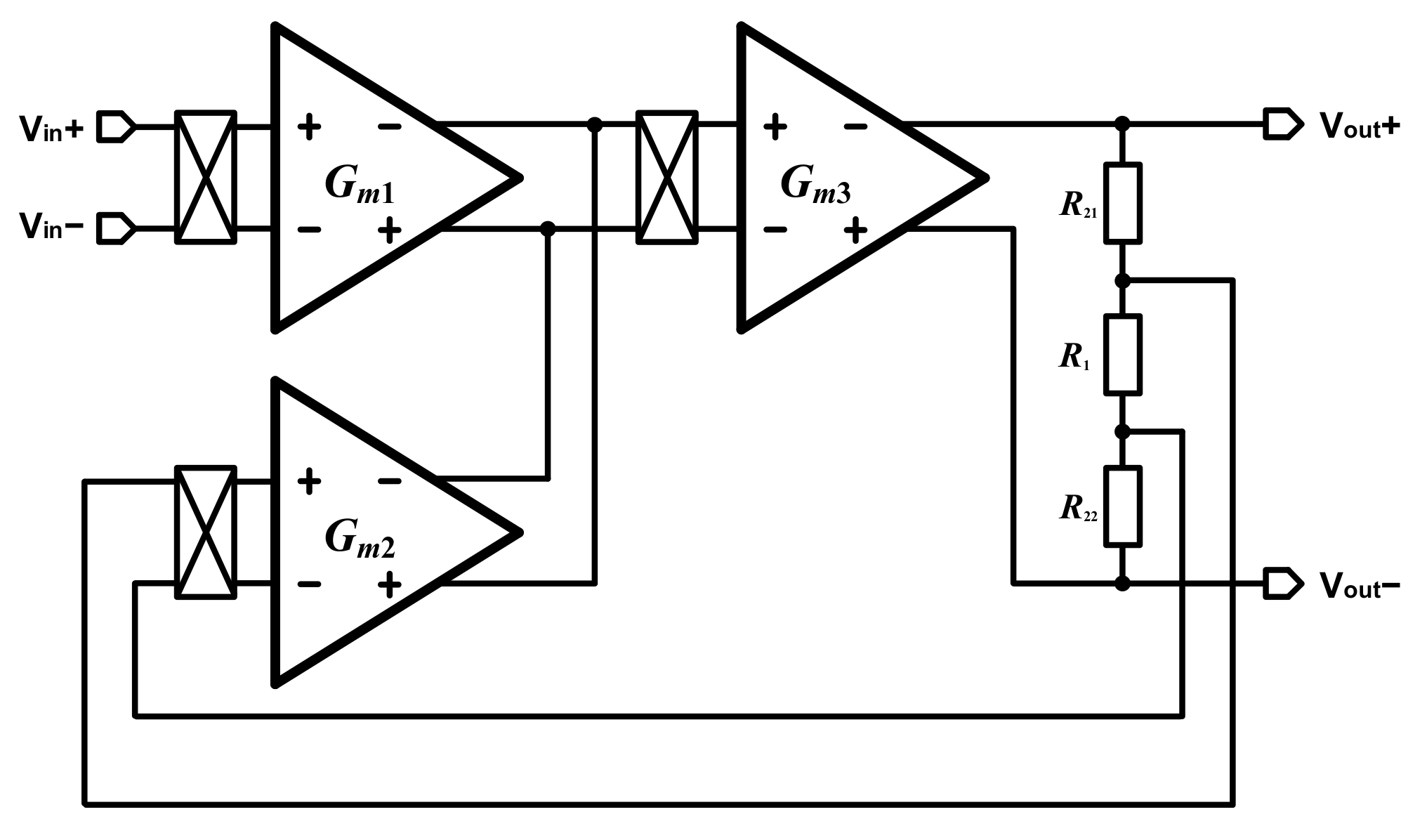
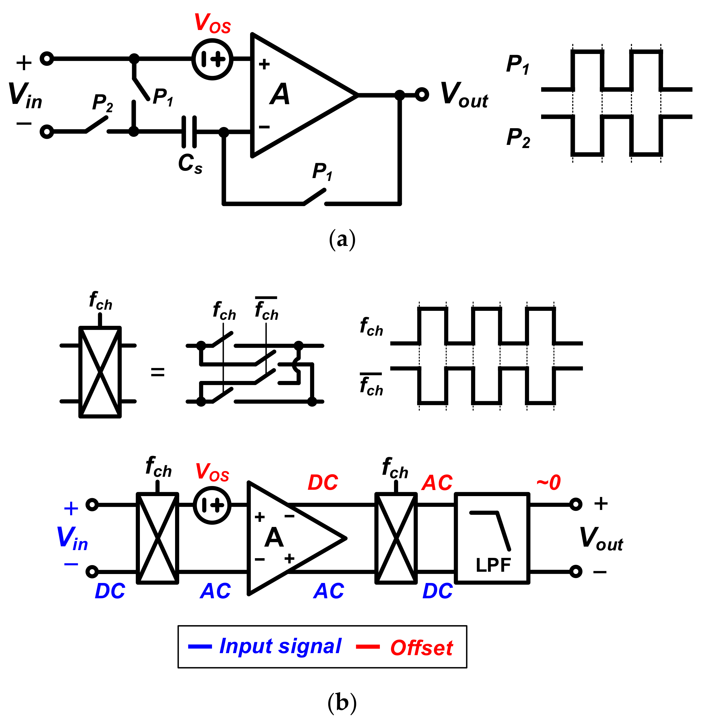
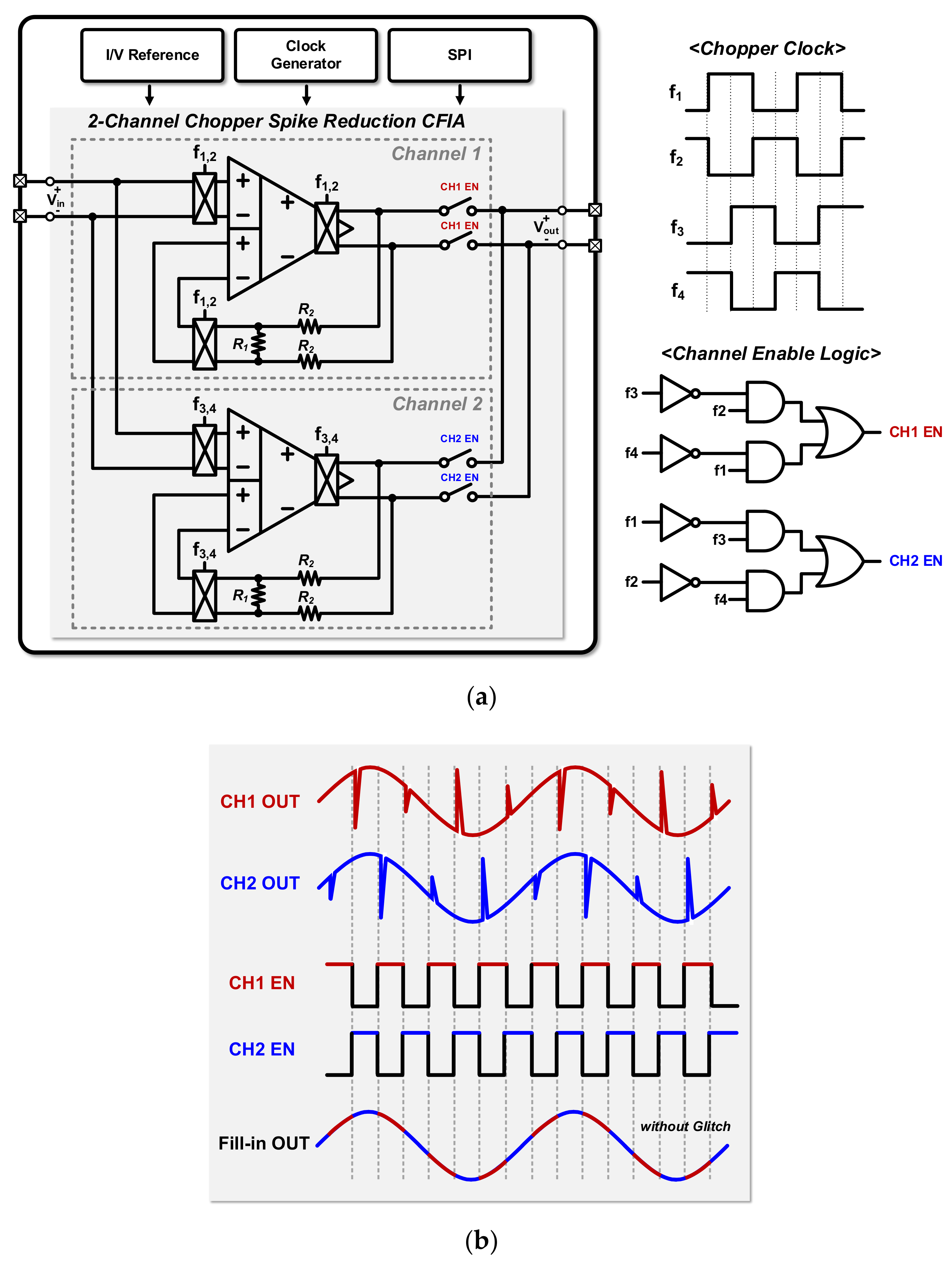
2.1. Top Architecture and Fill-In Technique of the Proposed CFIA

The top architecture of the proposed CFIA is illustrated in Figure 5a.
An on-chip I/V reference, clock generator, and SPI are included in the two-channel CFIA. The clock generator generates an 18 kHz chopper clock. Figure 5b illustrates the channel-enabled logic and timing. Each CFIA uses a different chopper clock (f1 and f2; f3 and f4). The chopper clock of channel 2 is delayed by 1/4 period relative to that of channel 1, as shown in Figure 5b. The glitch is generated at the end of each chopper clock, distorting the original signal. Enabling the two channels to send signals to the output alternately eliminates the glitch section and reduces distortion. Consequently, the final output signal does not contain a glitch.

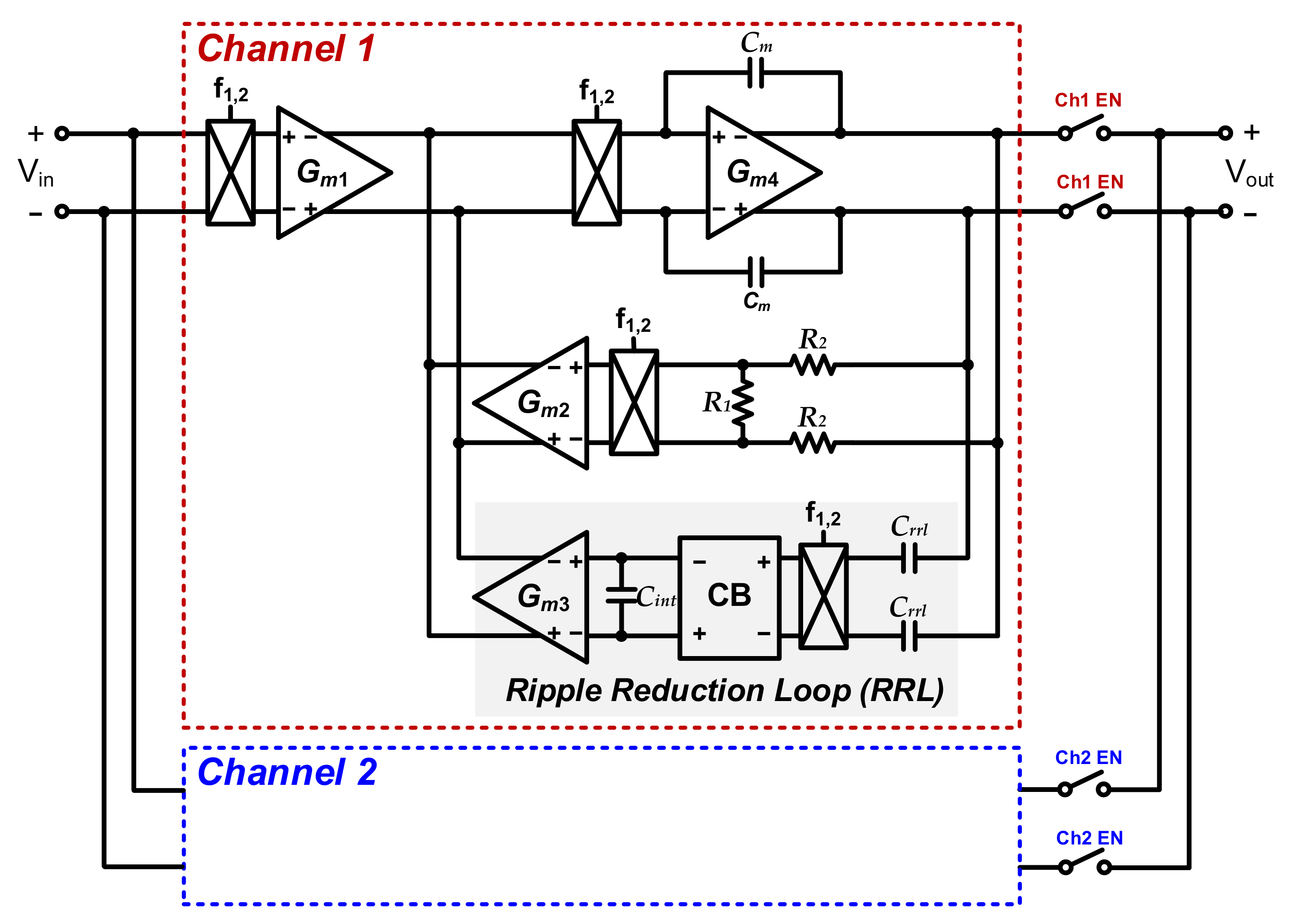
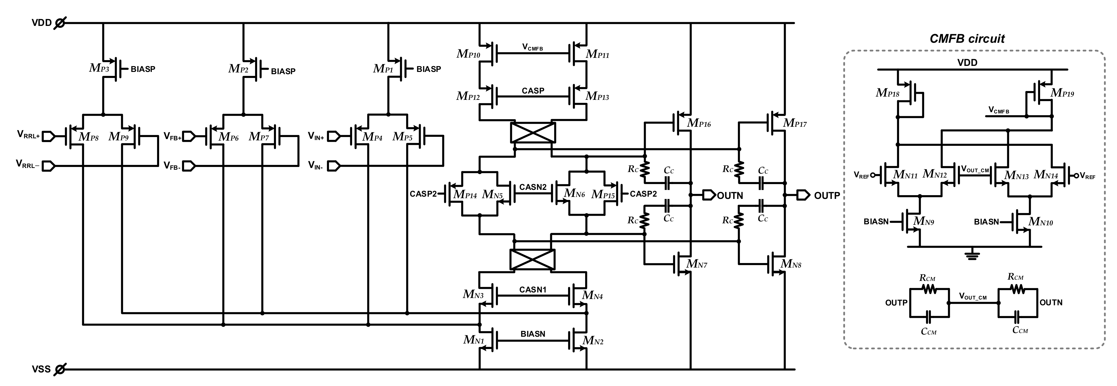
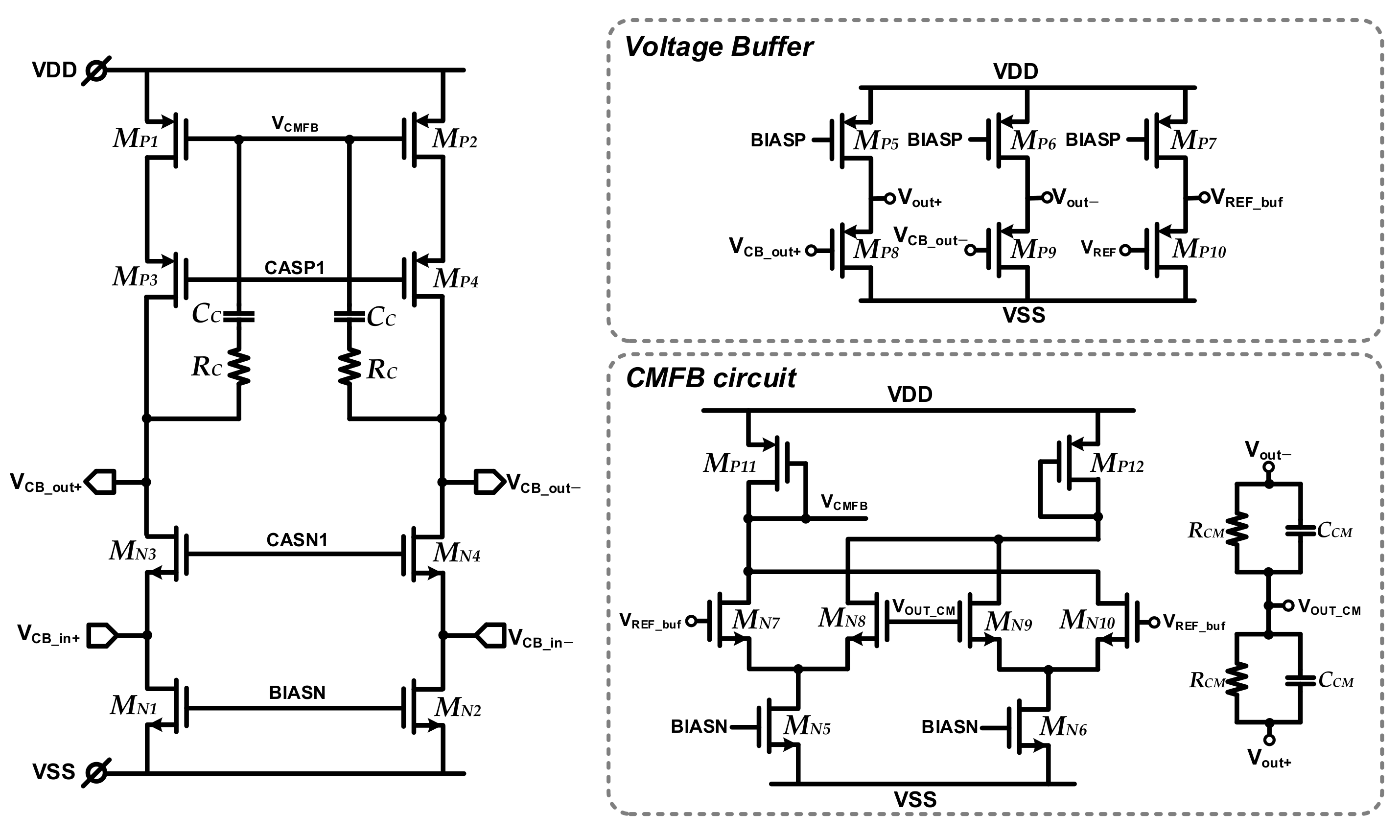
2.2. Configuration of the CFIA and RRL

A chopper was used at the input and before the integrator. The chopper-induced ripple caused by the input offset is one of the major drawbacks of the chopping technique. As shown in Figure 6, an RRL was added in this study to reduce ripple.
CH2 modulates the input offset of Gm1 to the chopper frequency as the offset current changes. After passing through the integrator, the ripple is displayed as a voltage at the output of Gm4. The capacitance (Crrls) detects the integrated ripple and converts it to current, followed by CH3 demodulation of the current offset. After passing through the current buffer, Cint converts the offset current to voltage, and Gm3 adds the opposite current to the offset current before sending it to the main amplifier.
Figure 7 depicts a schematic of the proposed CFIA at the transistor level. It includes a PMOS input stage, a folded cascode, and a Monticelli class-AB output stage. In addition, the RCMs and CCMs detect the output common-mode voltage in the common-mode feedback (CMFB) circuit. The current-mode error amplifier generates the control voltage (VCMFB), which adjusts the common-mode output voltage by biasing the gates of MP10 and MP11. A high open-loop gain of more than 100 dB reduces the finite gain error. In addition, a nested Miller capacitor was added to the CMFB stage and primary simplifier to ensure frequency stability with a 50° phase margin. Table 1 and Table 2 list the values of the transistors and the passive elements of the CFIA.
Figure 8 shows a schematic of the proposed current buffer used in the RRL. Table 3 and Table 4 list the values of the transistors and passive components in the current buffer, respectively.
Table 5 is about the noise contribution of the proposed circuit. Most noise source is the thermal noise of the transistor and also has a flicker noise component in the feedback resistor of the CFIA.
Figure 9 shows the glitch reduction simulation results. Figure 9a shows that the fill-in differential output reduced chopper glitches in the time domain. The simulation results for glitch reduction in the frequency domain are displayed in Figure 9b. The fill-in differential output reduced chopper glitch by 78 dB compared with the differential output of each channel when using an 18 kHz chopper frequency with 10 mV and 1 kHz sine input.
Figure 10 shows the corner simulation of the CMRR and power supply rejection ratio (PSRR). The value of the CMRR and PSRR at 10 Hz varies from 247.3 dB (at the FF 70 °C) to 271.9 dB (at the TT 27 °C) and 233.9 dB (at the FF 70 °C) to 258 dB (at the TT 27 °C), respectively. Figure 11 and Figure 12 show the Monte Carlo simulation result of the CMRR, PSRR, and input offset. The value of the CMRR and PSRR at 100 Hz with mismatch is 128.7 dB and 105.3 dB, respectively. The input mean offset has a value of 4.7 μV with the 200 samples.

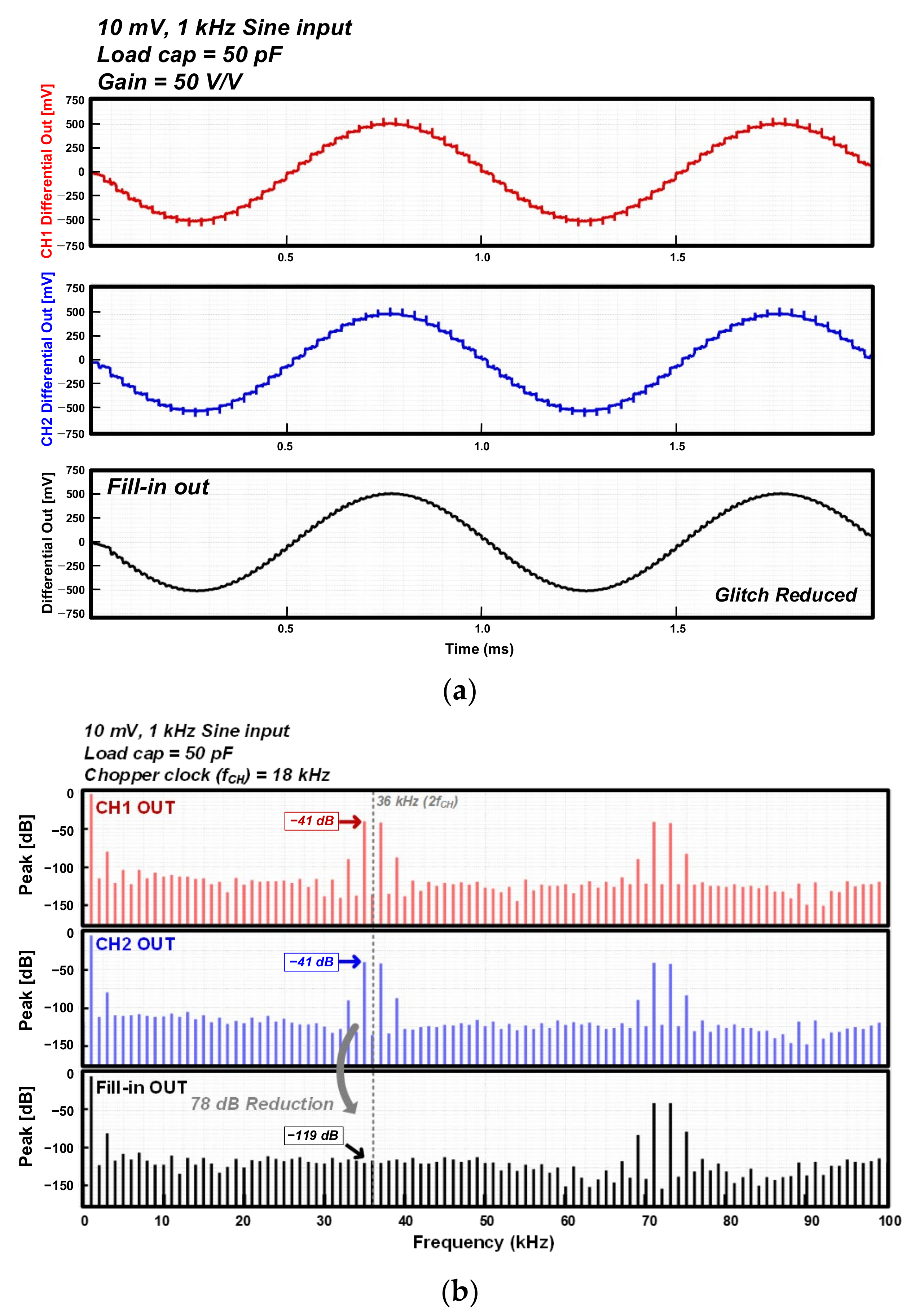
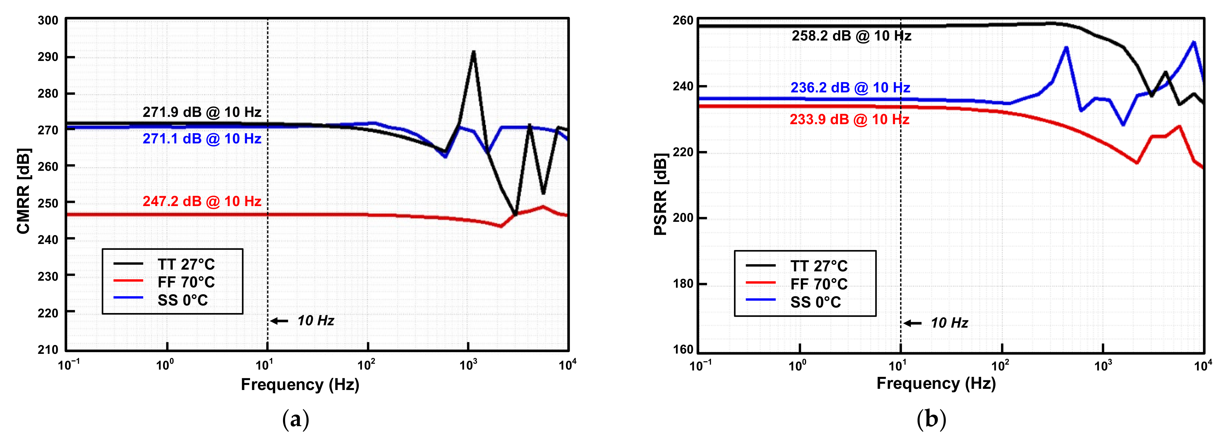
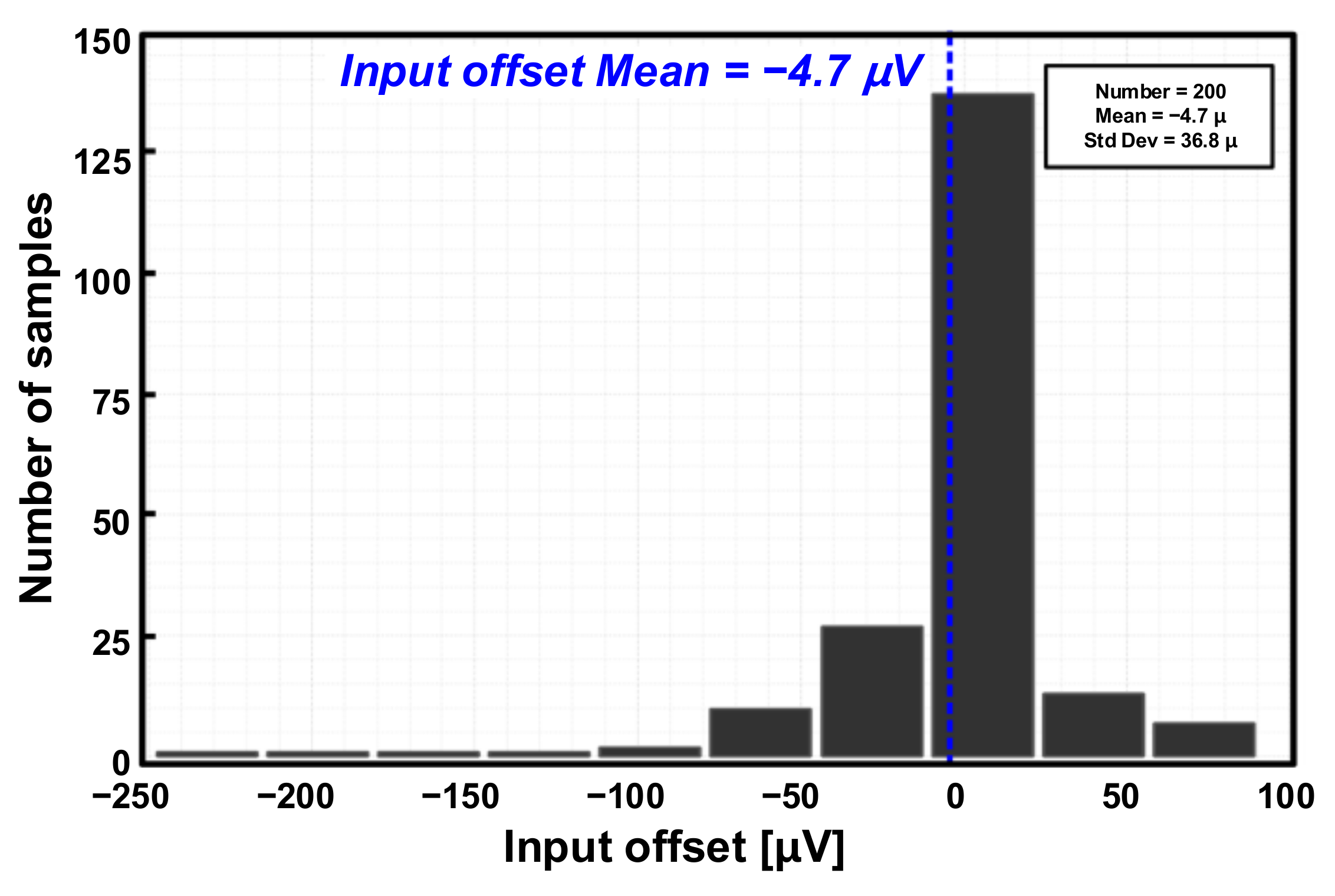
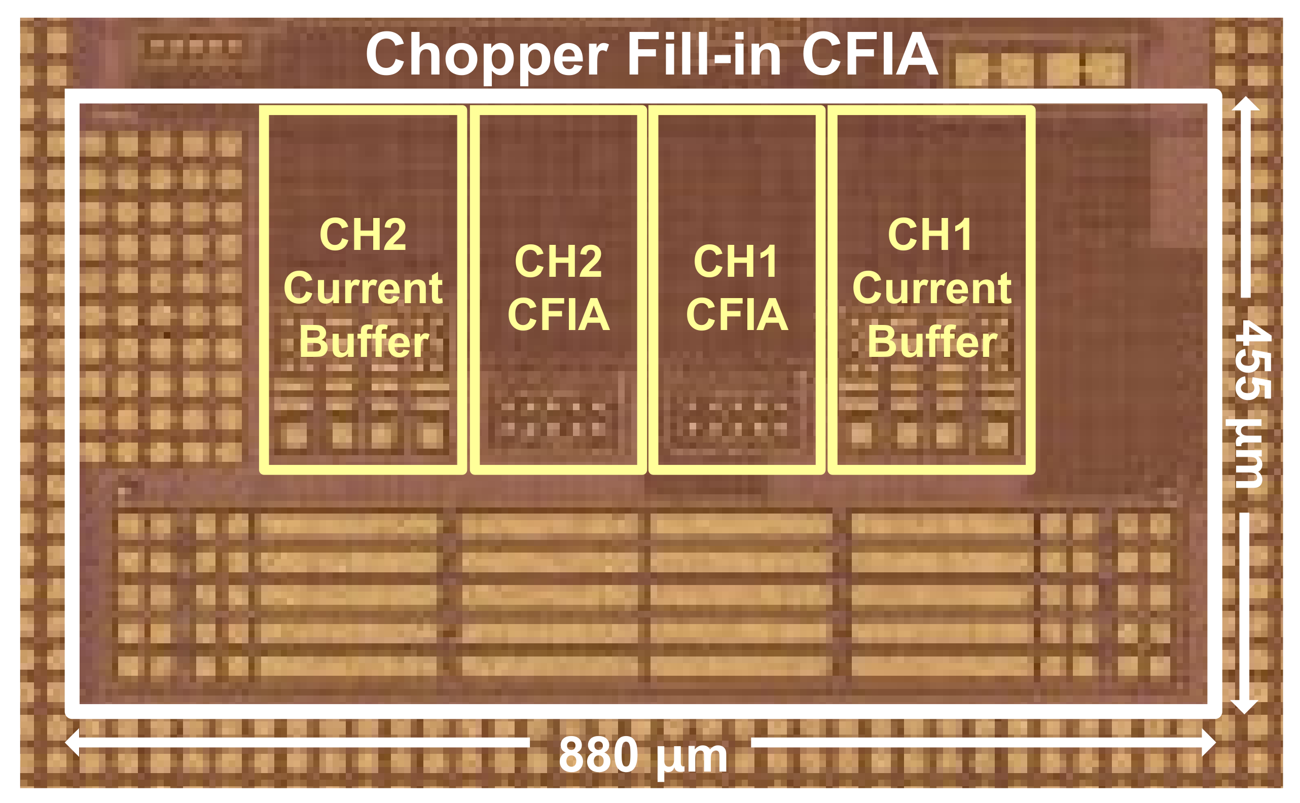
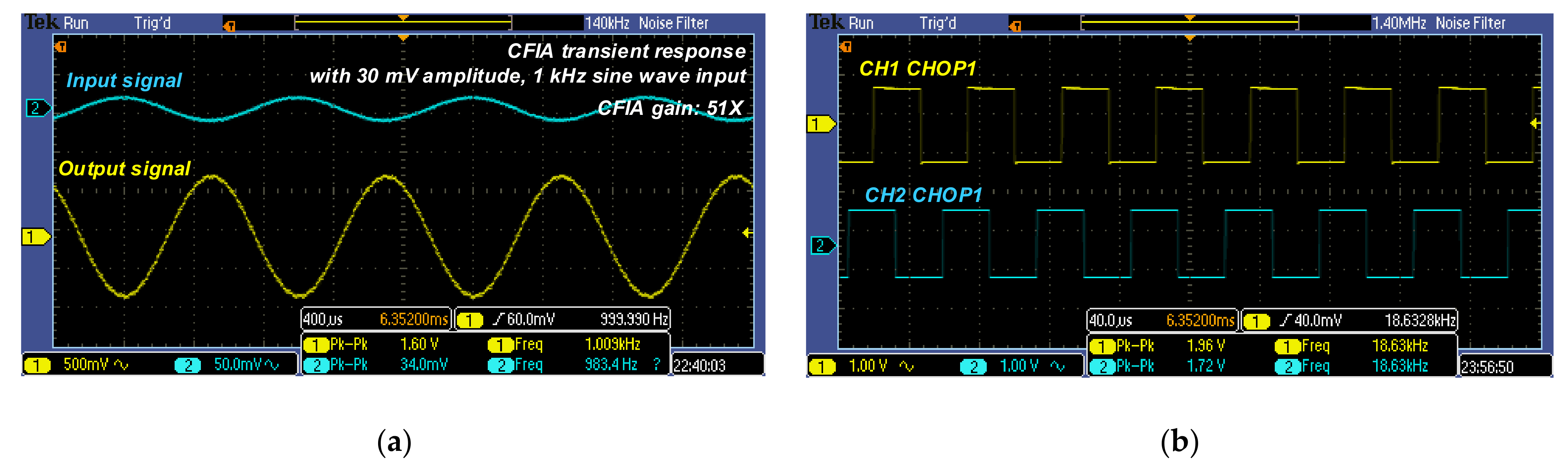
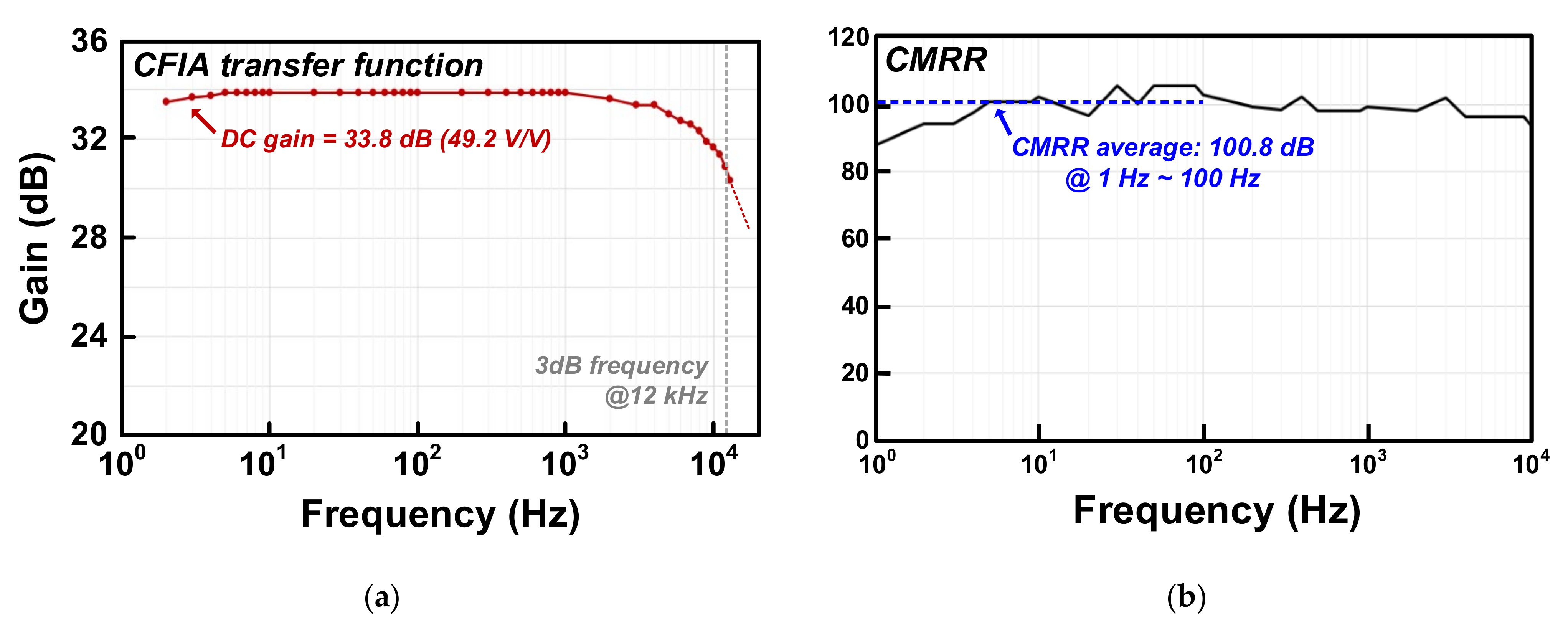
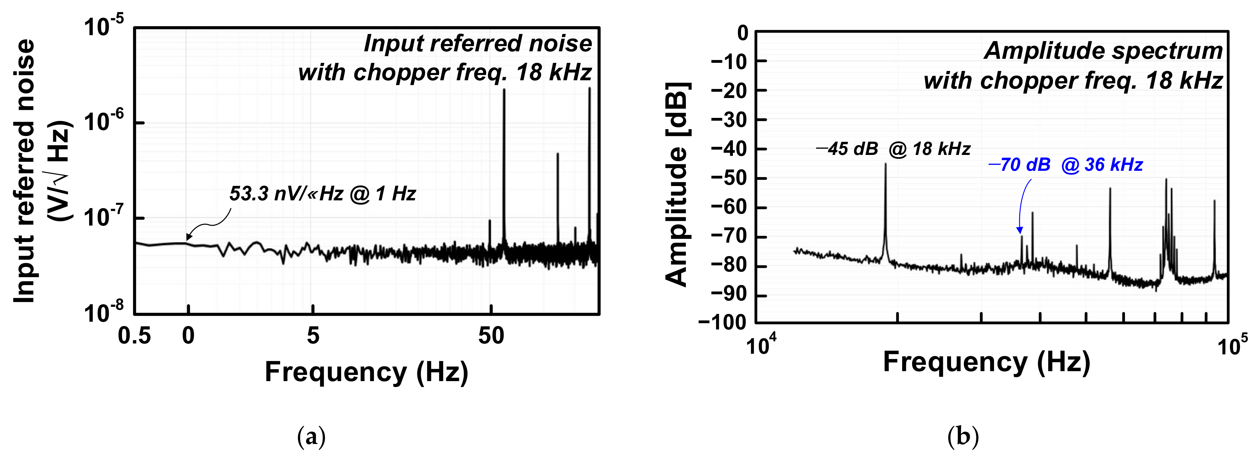
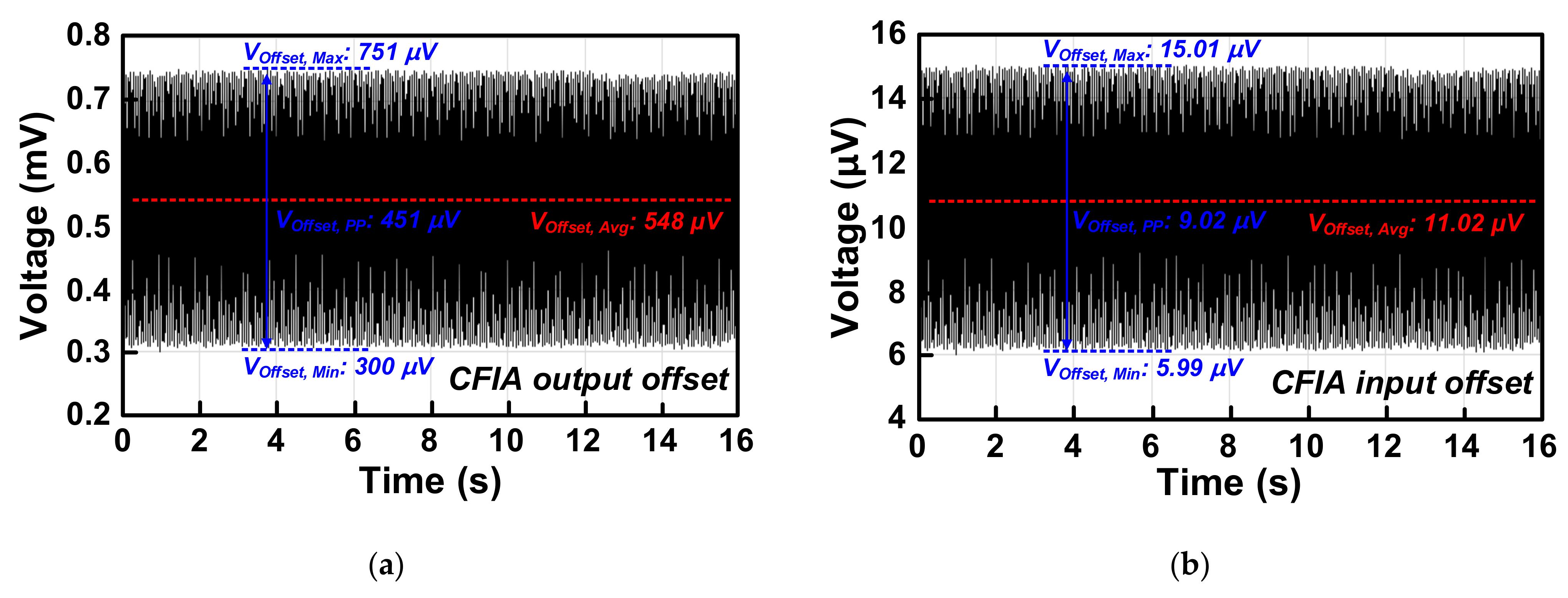
3. Measurement Results

A die photograph of the proposed CFIA is shown in Figure 13. The circuit was fabricated using a 0.18 µm CMOS process, and the area of the proposed chopper fill-in CFIA circuit is 455 × 880 µm.
Figure 14 depicts the test board and measurement environment used to evaluate the performance of the proposed CFIA using a printed circuit board.
The transient result of the proposed CFIA is shown in Figure 15. The proposed CFIA had an ideal gain of 51 V/V. As shown in Figure 15a, an input sine signal of 30 mVpeak-to-peak and 1 kHz was amplified to a 1.6-Vpeak-to-peak sine signal. The chopper clocks of channels 1 and 2 have a 1/4 phase difference, as shown in Figure 15b, and the proposed circuit uses a chopper frequency of 18 kHz.
Figure 16a represents the measurement results of the proposed CFIA transfer function. The transfer function has an average DC gain of 33.8 dB (49.2 V/V) and a 3-dB frequency of 12 kHz at 30.9 dB, resulting in a gain bandwidth (GBW) of 420 kHz. Figure 16b shows the CMRR measurement results of the proposed CFIA. The average CMRR from 1 Hz to 100 Hz is 100.8 dB.
Figure 17a presents the measured input-referred noise of the proposed CFIA; at 1 Hz, its value was 53.3 nV/√Hz. For the IMD tone amplitude measurement, 1 kHz and 10 mV sine inputs were used. As shown in Figure 17b, the measured amplitude of the IMD tone a twice the chopper frequency of 36 kHz with a chopper frequency of 18 kHz is −70 dB.
The measured output and input offset of the proposed CFIA is shown in Figure 18. The output offset measurement result shows that an average offset of 548 µV is present in the output of the CFIA and has a peak-to-peak value of 451 µV. Figure 18b shows the result of converting the measured output offset of the CFIA into input offset, which has an input average offset of 11.02 µV.
The calculated noise efficiency factor (NEF) for the proposed CFIA is 4.4. Table 6 shows a performance summary and comparison of the proposed circuit with other previous works on low-noise CFIAs.

4. Conclusions and Discussion

In this study, we present a dual-chopper CFIA with an RRL for glitch reduction. The chopping technique was used to obtain noise characteristics in the amplifier. However, glitches caused by chopping occur at each edge of the chopper clock, resulting in glitch-induced IMD. Owing to the input offset, the chopping technique also produces ripples.
Glitch-induced IMD was reduced in this study using a fill-in technique, whereby only neat signals were alternately used as outputs by avoiding the glitch section with a dual-chopping channel CFIA. By using the dual channel, it was possible to obtain an effect of noise reduction according to the noise correlation factor between channels. The RRL was implemented to reduce the ripple caused by chopping so that a high-order LPF was not required.
The proposed CFIA is based on a low-noise chopper fully differential difference amplifier with a cascode stage and a Monticelli class-AB output stage, which can drive a larger load and increase power efficiency.
The proposed dual-chopper CFIA was constructed using a standard 0.18 µm CMOS process, occupying an effective area of 1.28 mm2, and its current consumption with a 1.8-V power supply is 29.5 μA. The proposed CFIA had a gain of 51 V/V and GBW of 420 kHz. The input-referred noise at 1 Hz was 53.3 nV/√Hz, and integrated noise was 24.7 nV/√Hz, with an NEF of 4.48. The CMRR and PSRR have values of 108.8 dB and 105.3 dB at 100 Hz, respectively. The input offset is 11 μV, with a 51 V/V gain. The IMD amplitude at the chopper frequency harmonic is -70 dB.

Author Contributions

Conceptualization and supervision, H.K.; investigation and writing—original draft preparation, G.C.; writing—review and editing, K.N., M.Y., S.K., B.J., K.K. and H.S. All authors have read and agreed to the published version of the manuscript.

Funding

This work was supported (funded) by Nanomedical Devices Development Project of NNFC (CP22021M). This research was supported by the MSIT (Ministry of Science and ICT), Korea, under the ITRC (Information Technology Research Center) support program (IITP-2021-2017-0-01635) supervised by the IITP (Institute for Information & Communications Technology Planning & Evaluation). This study was supported by a National Research Foundation of Korea (NRF) grant funded by the Korean government (MSIT) (No. 2022R1A2C100517011).

Institutional Review Board Statement

Not applicable.

Informed Consent Statement

Not applicable.

Data Availability Statement

Not applicable.

Acknowledgments

The EDA tool was supported by the IC Design Education Center (IDEC) in Korea.

Conflicts of Interest

The authors declare no conflict of interest.

Abbreviations

The following abbreviations are used in this manuscript:
CFIAcurrent-feedback instrumentation amplifier
IMDintermodulation distortion
IAinstrumentation amplifier
AFEanalog front end
CMRRcommon-mode rejection ratio
DOCdynamic offset compensation
AZauto-zeroing
OTAoperational transconductance amplifier
LPFlow-frequency filter
RRLripple reduction loop
CMFBcommon-mode feedback
PSRRpower supply rejection ratio
GBWgain bandwidth
NEFnoise efficiency factor

References

  1. Ong, G.T.; Chan, P.K. A Power-Aware Chopper-Stabilized Instrumentation Amplifier for Resistive Wheatstone Bridge Sensors. IEEE Trans. Intrum. Meas. 2014, 63, 2253–2263. [Google Scholar] [CrossRef]
  2. Ahmad, M.; Malik, S.; Dewan, S.; Bose, A.K.; Maddipatla, D.; Narakathu, B.B.; Atashbar, M.Z.; Baghini, M.S. An auto-calibrated resistive measurement system with low noise instrumentation ASIC. IEEE J. Solid-State Circuits 2020, 55, 3036–3050. [Google Scholar] [CrossRef]
  3. Sharma, B.P.; Mehra, R. Design of CMOS instrumentation amplifier with improved gain & CMRR for low power sensor applications. In Proceedings of the 2016 2nd International Conference on Next Generation Computing Technologies (NGCT), IEEE Conference, Dehradun, India, 14–16 October 2016. [Google Scholar]
  4. Pertijs, M.A.P.; Kindt, W.J. A 140 dB-CMRR Current-Feedback Instrumentation Amplifier Employing Ping-Pong Auto-Zeroing and Chopping. IEEE J. Solid-State Circuits 2010, 45, 2044–2056. [Google Scholar] [CrossRef]
  5. Archanaa, M.; Balamurugan, K. Analysis of thermal noise and noise reduction in CMOS device. In Proceedings of the 2014 International Conference on Green Computing Communication and Electrical Engineering (ICGCCEE), IEEE Conference, Coimbatore, India, 6–8 March 2014. [Google Scholar]
  6. Witte, J.F.; Huijising, J.H.; Makinwa, K.A.A. A Chopper and Auto-Zero Offset-Stabilized CMOS Instrumentation Amplifier. In Proceedings of the 2009 Proceedings of the 2009 Symposium on VLSI Circuits, Kyoto, Japan, 16–18 June 2009. [Google Scholar]
  7. Rooijers, T.; Karmakar, S.; Kusuda, Y.; Huijising, J.H.; Makinwa, K.A.A. A Fill-In Technique for Robust IMD Suppression in Chopper Amplifiers. IEEE J. Solid-State Circuits 2021, 56, 3583–3592. [Google Scholar] [CrossRef]
  8. Vejdani, P.; Nabki, F. Dual-Path and Dual-Chopper Amplifier Signal Conditioning Circuit with Improved SNR and Ultra-Low Power Consumption for MEMS. IEEE Trans Circuit Syst I Regul Pap IEEE T Circuits-I 2019, 66, 2253–2262. [Google Scholar] [CrossRef]
  9. Yoo, M.; Kwon, Y.; Kim, H.; Choi, G.; Nam, K.; Ko, H. Low-Noise Resistive Bridge Sensor Analog Front-End Using Chopper-Stabilized Multipath Current Feedback Instrumentation Amplifier and Automatic Offset Cancellation Loop. IEEE Access 2022, 10, 12385–12394. [Google Scholar] [CrossRef]
  10. Choi, G.; Heo, H.; You, D.; Kim, H.; Nam, K.; Yoo, M.; Lee, S.; Ko, H. A Low-Power, Low-Noise, Resistive-Bridge Microsensor Readout Circuit with Chopper-Stabilized Recycling Folded Cascode Instrumentation Amplifier. Appl. Sci. 2021, 11, 7982. [Google Scholar] [CrossRef]
  11. Kwon, Y.; Kim, H.; Kim, J.; Han, K.; You, D.; Heo, H.; Cho, D.; Ko, H. Fully Differential Chopper-Stabilized Multipath Current-Feedback Instrumentation Amplifier with R-2R DAC Offset Adjustment for Resistive Bridge Sensors. Appl. Sci. 2020, 10, 63. [Google Scholar] [CrossRef] [Green Version]
Figure 1. Conventional CFIA structure with a chopper.
Applsci 12 10471 g001
Figure 2. Conventional DOC techniques: (a) AZ and (b) chopping.
Applsci 12 10471 g002
Figure 3. Drawbacks of the chopping technique: (a) ripple and (b) glitch.
Applsci 12 10471 g003
Figure 4. Diagram of the noise voltage summation of the amplifiers in the dual path.
Applsci 12 10471 g004
Figure 5. (a) The top architecture of the proposed CFIA and (b) fill-in technique.
Applsci 12 10471 g005
Figure 6. CFIA and RRL configuration in one channel.
Applsci 12 10471 g006
Figure 7. Transistor-level schematic of the proposed CFIA.
Applsci 12 10471 g007
Figure 8. Schematic of the proposed current buffer in the RRL.
Applsci 12 10471 g008
Figure 9. Glitch reduction simulation result for the proposed CFIA: (a) transient simulation result and (b) amplitude spectrum.
Applsci 12 10471 g009
Figure 10. Corner simulation result of the (a) CMRR and (b) PSRR.
Applsci 12 10471 g010
Figure 11. Monte Carlo simulation results of the (a) CMRR and (b) PSRR.
Applsci 12 10471 g011
Figure 12. Monte Carlo simulation results of the input offset.
Applsci 12 10471 g012
Figure 13. Die photograph of the proposed CFIA.
Applsci 12 10471 g013
Figure 14. Measurement environment of the proposed CFIA with test board.
Applsci 12 10471 g014
Figure 15. (a) Sine wave amplification and (b) chopper clock transient response measurement result for the proposed CFIA.
Applsci 12 10471 g015
Figure 16. (a) Transfer function and (b) CMRR of the proposed CFIA.
Applsci 12 10471 g016
Figure 17. Experimental (a) input-referred noise and (b) amplitude spectrum of 1 kHz 10 mV sine input for IMD tone measurement.
Applsci 12 10471 g017
Figure 18. Measured (a) output offset and (b) input-referred offset.
Applsci 12 10471 g018
Table 1. Values of transistors in the proposed CFIA.
TransistorSize (W/L) (µm)TransistorSize (W/L) (µm)
MP1, MP218/3.2MN1, MN213.6/10
MP36/3.2MN3, MN45.6/4
MP4MP980/0.5MN5, MN62/14
MP10, MP1126/3MN7, MN82/1
MP12, MP1310/1MN9, MN102/5
MP14, MP154/9NM11MN1412/2
MP16, MP178/1
MP18, MP1920/2
Table 2. Values of the passive components in the proposed CFIA.
ComponentValue
CC412 fF
RC134 kΩ
RCM2.3 MΩ
CCM206 fF
Table 3. Values of transistors in the current buffer.
TransistorSize (W/L) (µm)TransistorSize (W/L) (µm)
MP1, MP212/3MN1, MN22.4/14
MP3, MP412/3MN3, MN43/4
MP5MP71/4MN5, MN61/8
MP8MP102/2MN7MN104/2
MP11, MP127/3
Table 4. Values of the passive components in the current buffer.
ComponentValue
CC1.2 pF
RC11.2 kΩ
RCM224 kΩ
CCM1.6 pF
Table 5. Simulated noise contribution.
TransistorNoise SourceTotal Noise (%)
MN1, MN2 (Figure 7)Thermal23.74
MP10, MP11 (Figure 7)Thermal9.26
MN6, MN7, MN8, MN9 (Figure 7)Thermal6.84
R1 (Figure 6)Flicker3.8
Table 6. Performance summary of the proposed CFIA and comparison with other studies.
This Work[9][10][11][4]
ArchitectureCFIACFIACFIACFIACFIA
Dynamic techniquechopping + fill-in + RRLMultipath +chopper stabilization +RRLRFC + choppingMultipath + chopper stabilization +RRLAuto-zeroing + chopping + ping-pong
Technology (µm)0.180.180.180.180.5
Supply voltage (V)1.83.31.81.83.0~5.0
Current consumption (µA)291232.231691700
Power consumption (mW)52.2405.94.014304.25100~8500
Active area (mm2)1.281.280.5361.42.5
Gain bandwidth (Hz)420 k1.92 M580 k59.2 k800 k
Input-referred noise (nV/√Hz)53.3 @1 Hz
24.7 (integrated)
1086.618.327
CMRR (dB)108.8>100176.6162142
PSRR (dB)105.3>90119112138
Offset (V)11 μ1 μ--2.8 μ
NEF *4.44.34.9414.213.5
* NEF = Vni√(2∙Itot/π∙UT∙4 kT∙BW).
Publisher’s Note: MDPI stays neutral with regard to jurisdictional claims in published maps and institutional affiliations.

