
Design of 2–16 GHz Non-Uniform Distributed GaN HEMT MMIC Power Amplifier with Harmonic Suppression Network

Abstract
:1. Introduction
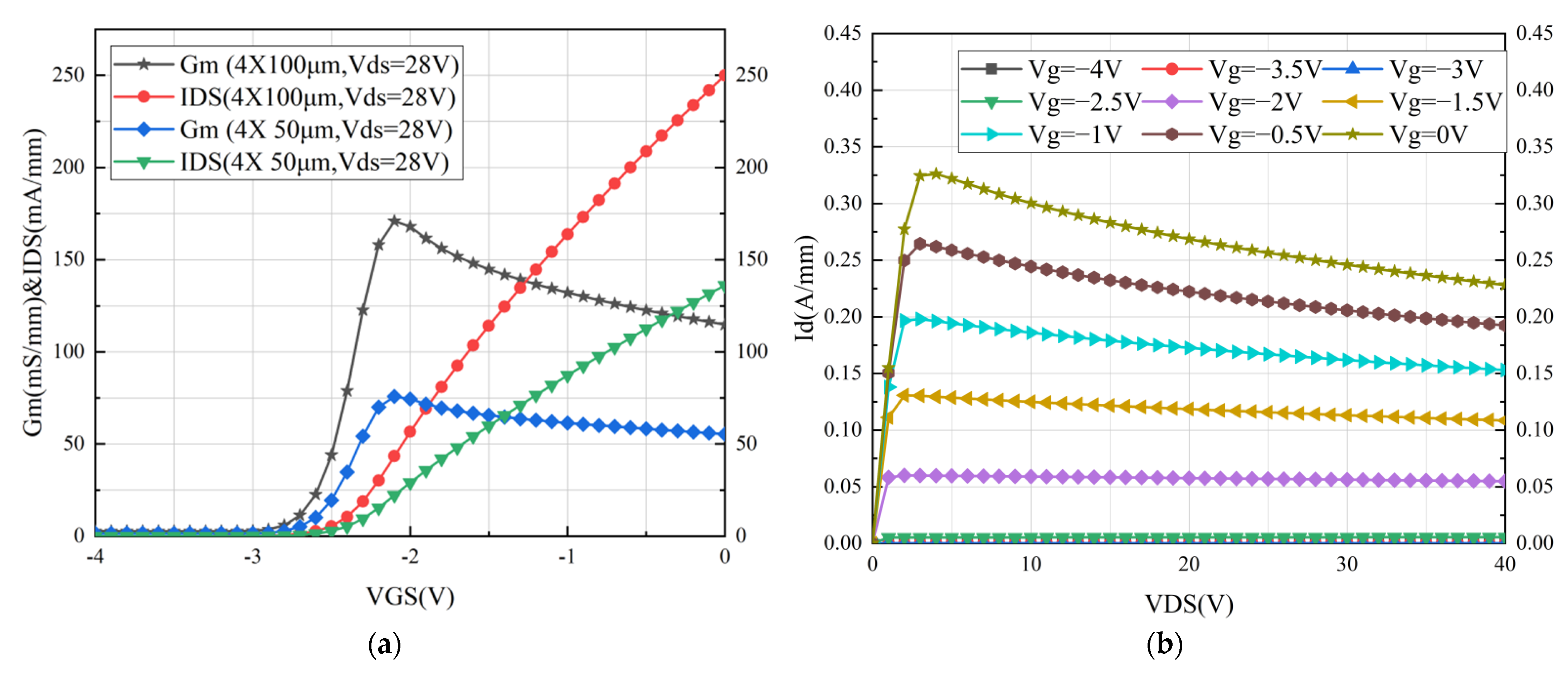
2. GaN on SiC HEMTs
3. Circuit Design
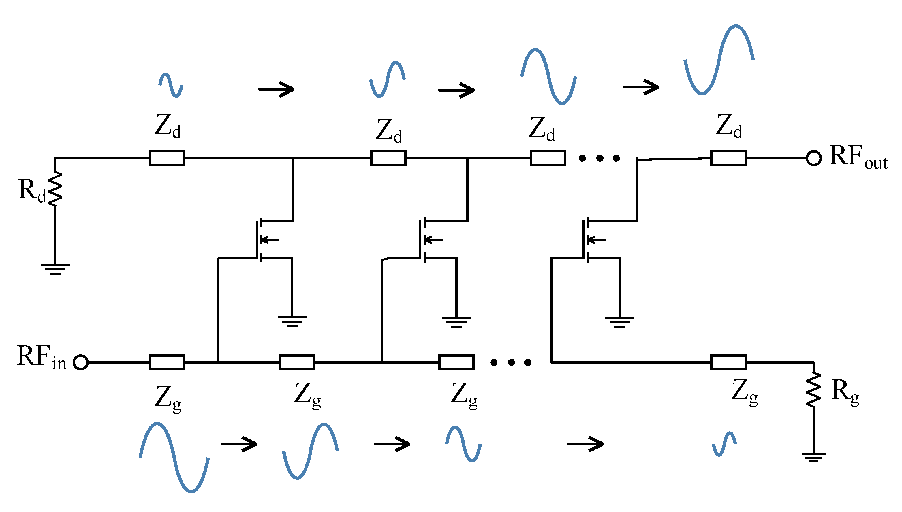
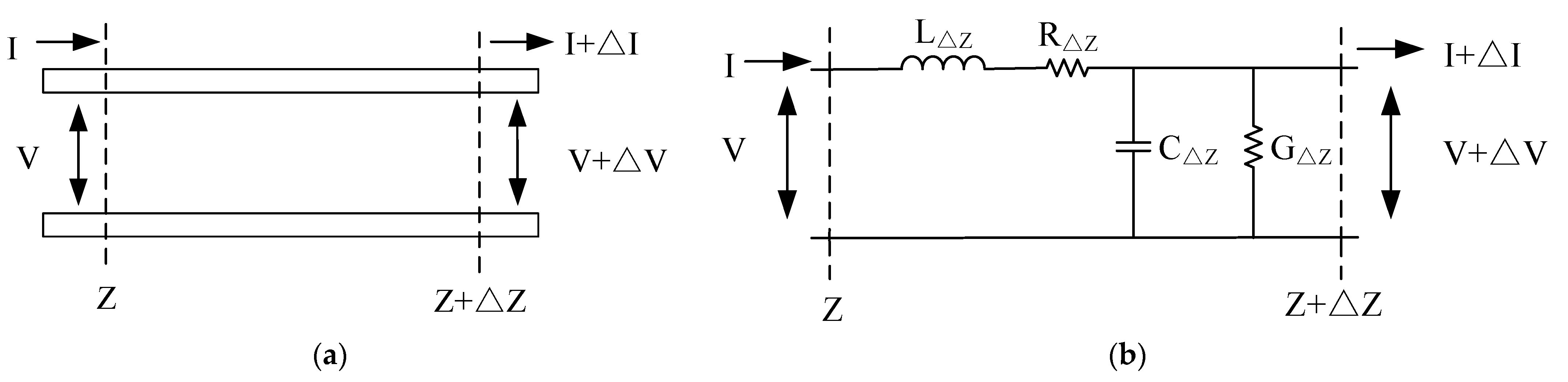
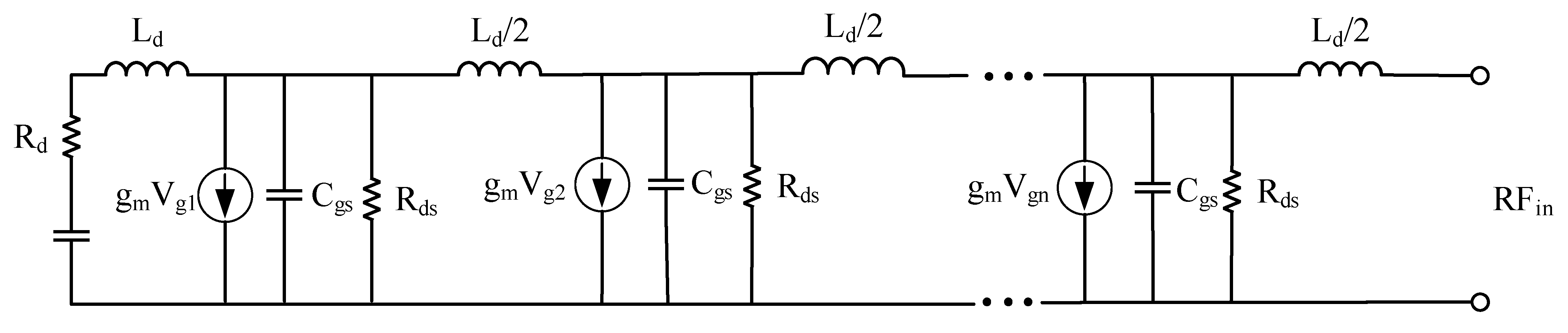
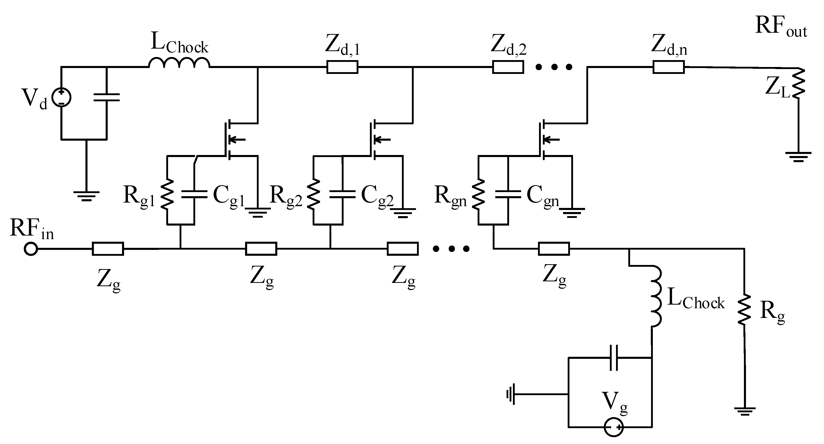
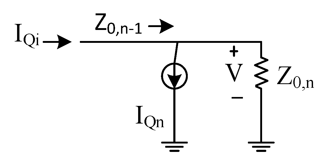
3.1. Principle of Distributed Amplifier
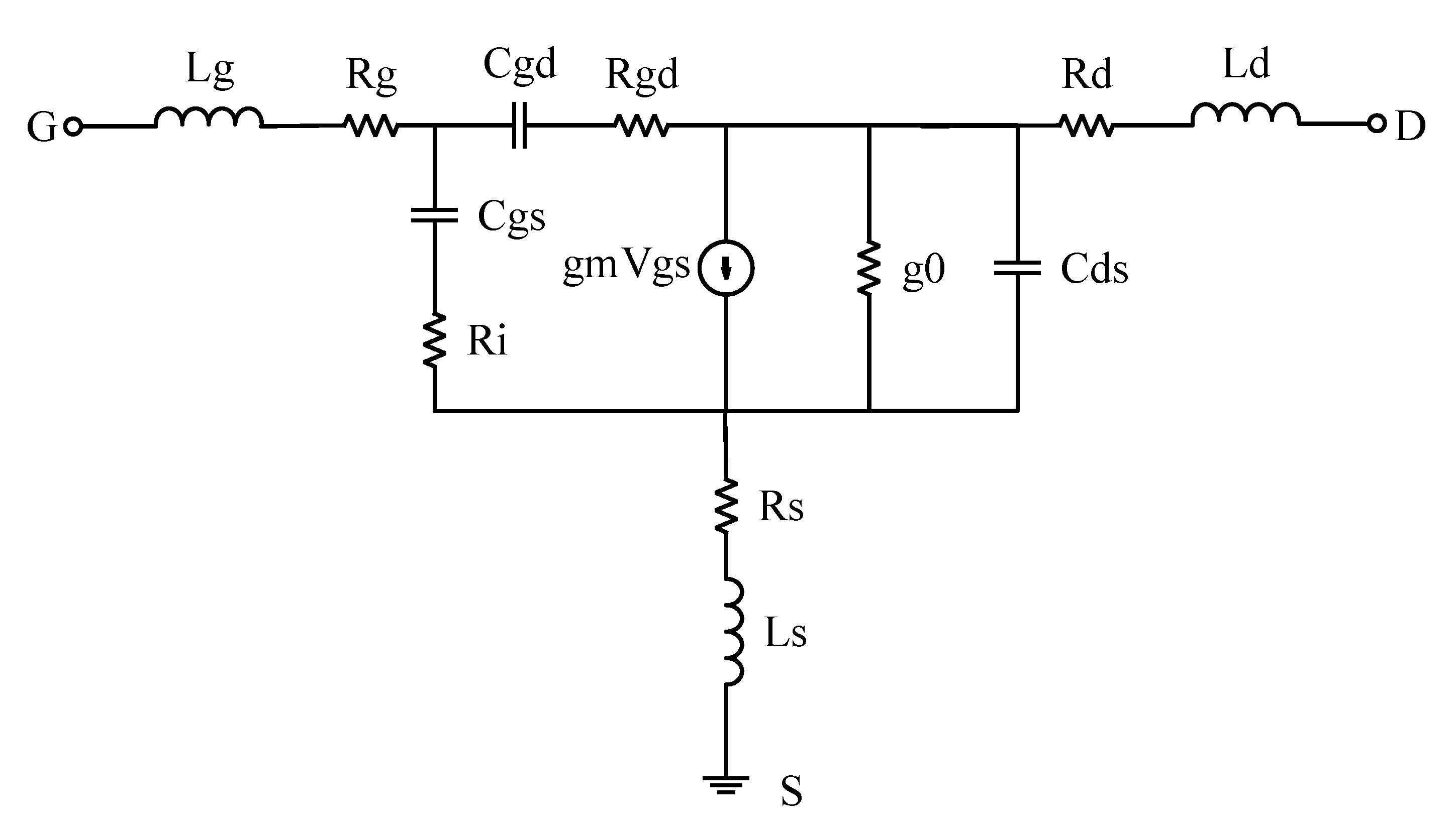
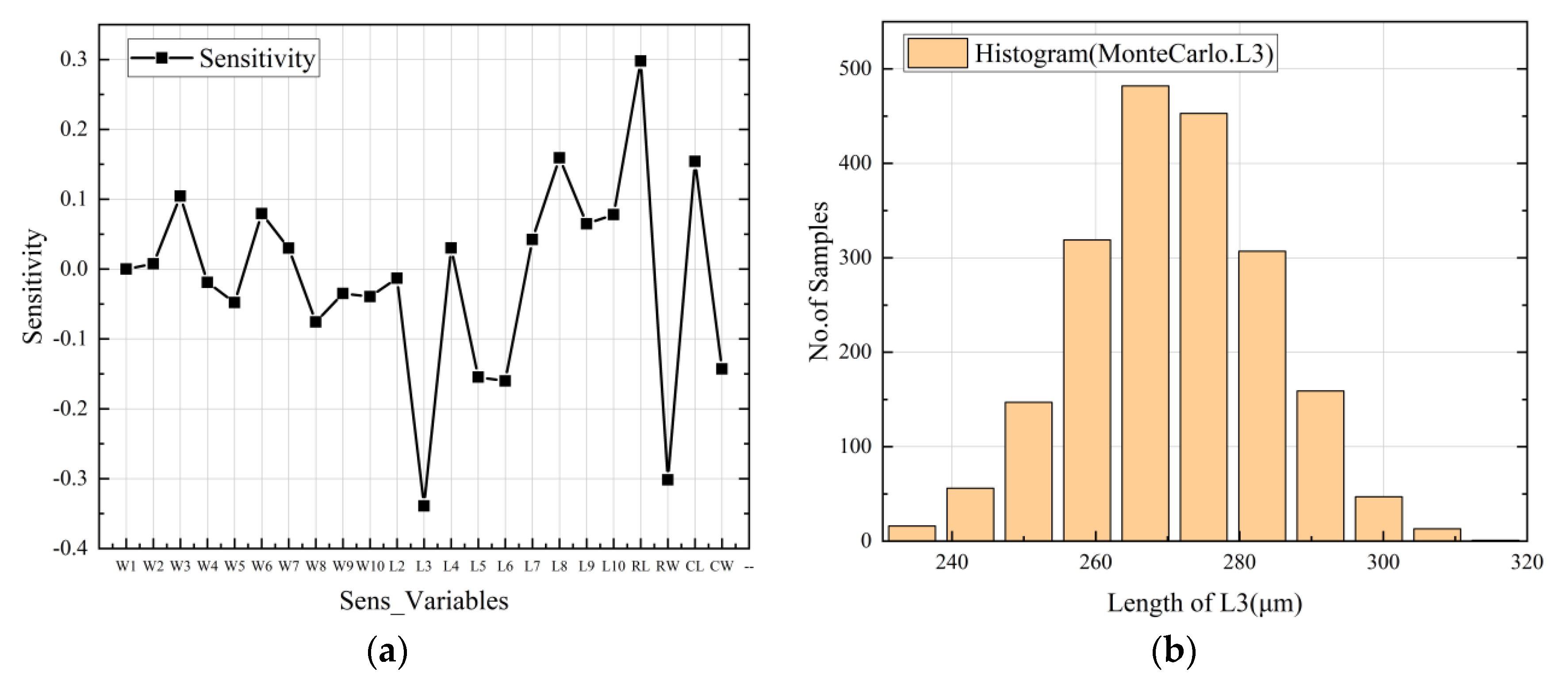
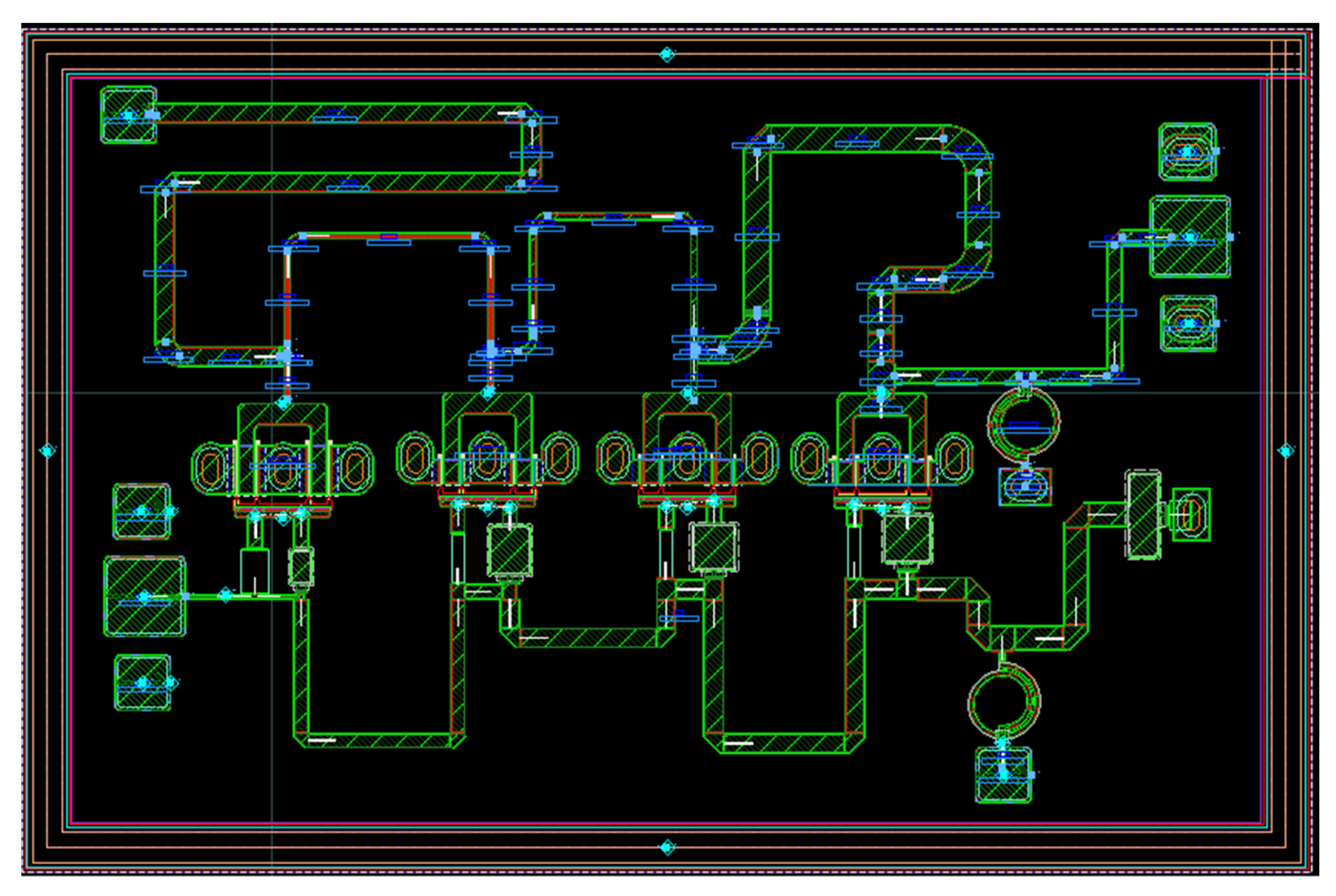
3.2. Simulation Analysis
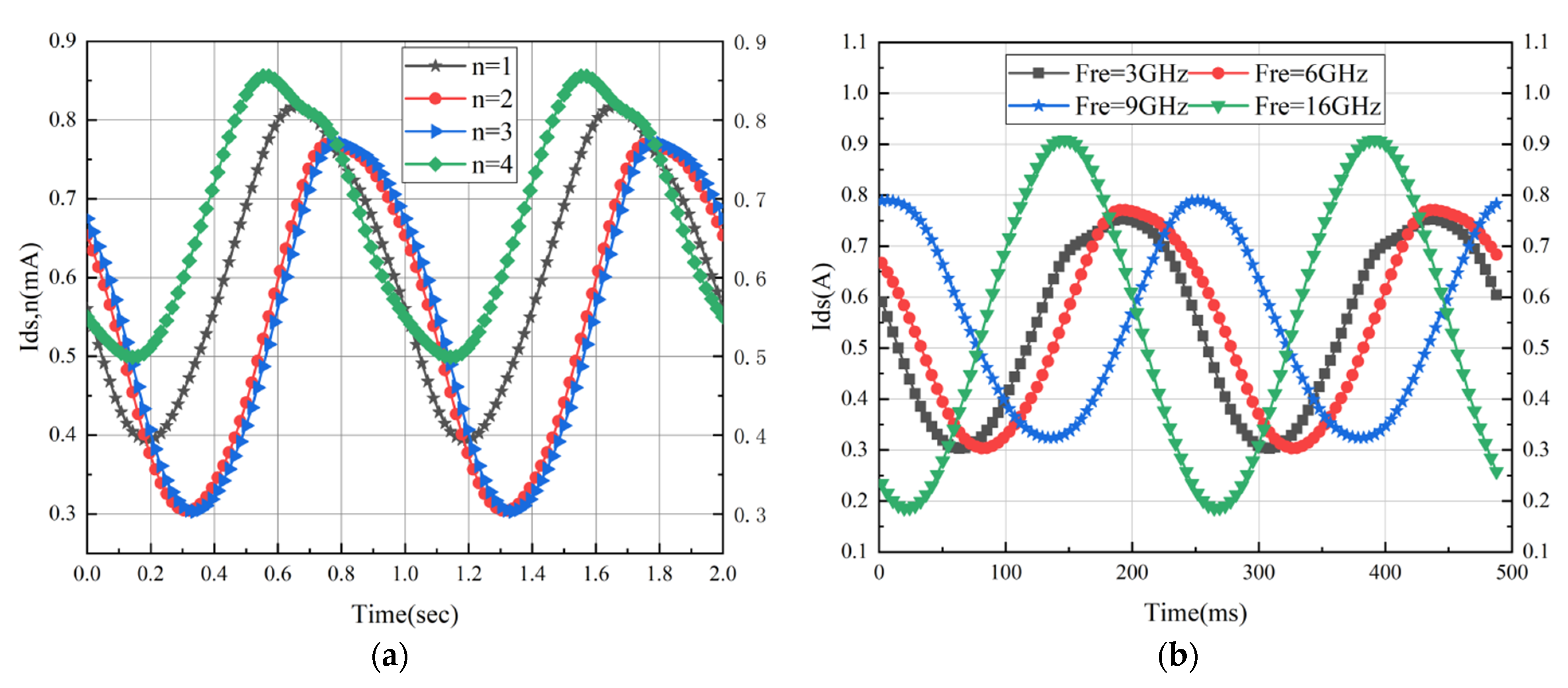
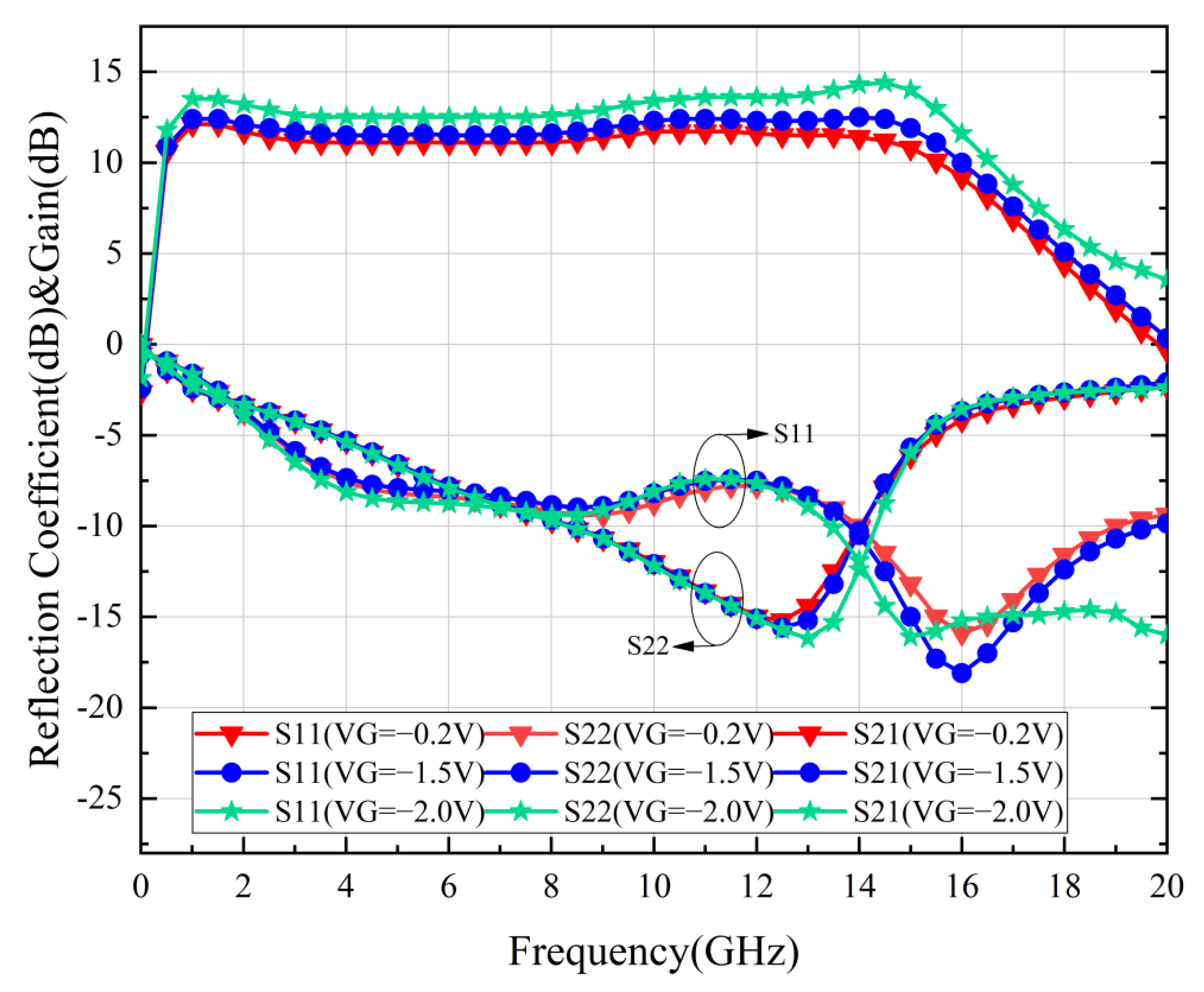
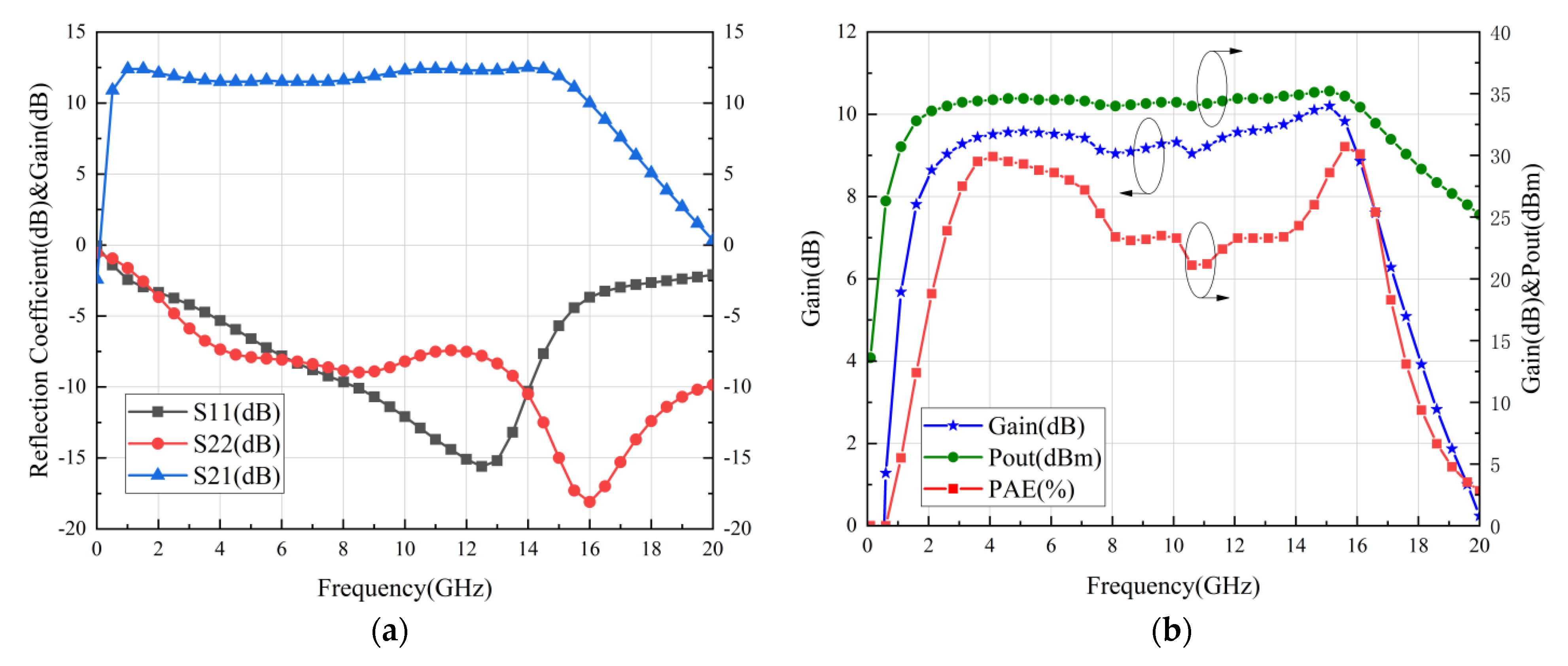
4. NDPA Simulation Results
5. Conclusions
Author Contributions
Funding
Institutional Review Board Statement
Informed Consent Statement
Data Availability Statement
Conflicts of Interest
References
- Campbell, C.F.; Nayak, S.; Kao, M.-Y.; Chen, S. Design and performance of 16–40GHz GaN distributed power amplifier MMICs utilizing an advanced 0.15 µm GaN process. In Proceedings of the 2016 IEEE MTT-S International Microwave Symposium (IMS), San Francisco, CA, USA, 22–27 May 2016; pp. 1–4. [Google Scholar]
- Mahon, S.J.; Milner, L.E.; Shahid, I.; Parker, A.E.; Gorman, M.C.; Heimlich, M.C. High Power Density 4 to 16 GHz Non-Uniform Distributed Power Amplifier with a Novel Trifilar. In Proceedings of the 2020 15th European Microwave Integrated Circuits Conference (EuMIC), Utrecht, The Netherlands, 11–12 January 2021; pp. 273–276. [Google Scholar]
- Kim, J.; Kwon, Y. A High-Performance GaN-Modified Nonuniform Distributed Power Amplifier. IEEE Trans. Microw. Theory Tech. 2020, 68, 1729–1740. [Google Scholar] [CrossRef]
- Campbell, C.F.; Roberg, M.D.; Fain, J.; Nayak, S. A 1–8 GHz Gallium Nitride distributed power amplifier MMIC utilizing a trifilar transformer. In Proceedings of the 2016 11th European Microwave Integrated Circuits Conference (EuMIC), London, UK, 3–4 October 2016; pp. 217–220. [Google Scholar]
- Huang, F.; Chen, W.; Wang, D.; Feng, Z. A Broadband GaN Power Amplifier MMIC Utilizing a Non-Uniform Distributed Topology. In Proceedings of the 2019 IEEE MTT-S International Wireless Symposium (IWS), Guangzhou, China, 19–22 May 2019; pp. 1–3. [Google Scholar]
- Zhou, X.; Roy, L.; Amaya, R.E. 1 W, Highly Efficient, Ultra-Broadband Non-Uniform Distributed Power Amplifier in GaN. IEEE Microw. Wirel. Compon. Lett. 2013, 23, 208–210. [Google Scholar] [CrossRef]
- Ginzton, E.L.; Hewlett, W.R.; Jasberg, J.H.; Noe, J.D. Distributed Amplification. Proc. IRE 1948, 36, 956–969. [Google Scholar] [CrossRef]
- Roberg, M.; Schafer, S.; Marrufo, O.; Hon, T. A 2–20 GHz Distributed GaN Power Amplifier Using a Novel Biasing Technique. In Proceedings of the 2019 IEEE MTT-S International Microwave Symposium (IMS), Boston, MA, USA, 2–7 June 2019; pp. 694–697. [Google Scholar]
- Campbell, C.; Lee, C.; Williams, V.; Kao, M.Y.; Tserng, H.Q.; Saunier, P.; Balisteri, T. A Wideband Power Amplifier MMIC Utilizing GaN on SiC HEMT Technology. IEEE J. Solid-State Circuits 2009, 44, 2640–2647. [Google Scholar] [CrossRef]
- Campbell, C.; Lee, C.; Williams, V.; Kao, M.-Y.; Tserng, H.-Q.; Saunier, P. A Wideband Power Amplifier MMIC Utilizing GaN on SiC HEMT Technology. In Proceedings of the 2008 IEEE Compound Semiconductor Integrated Circuits Symposium, Portland, OR, USA, 14–17 October 2008; pp. 1–4. [Google Scholar]
- Duperrier, C.; Campovecchio, M.; Roussel, L.; Lajugie, M.; Quere, R. New design method of uniform and nonuniform distributed power amplifiers. IEEE Trans. Microw. Theory Tech. 2001, 49, 2494–2500. [Google Scholar] [CrossRef]
- Podgorski, A.S.; Wei, L.Y. Theory of traveling-wave transistors. IEEE Trans. Electron Devices 1982, 29, 1845–1853. [Google Scholar] [CrossRef]
- Zhang, F.; Kinget, P.R. Low-power programmable gain CMOS distributed LNA. IEEE J. Solid-State Circuits 2006, 41, 1333–1343. [Google Scholar] [CrossRef]
- Campbell, C.F. Evolution of the Nonuniform Distributed Power Amplifier: A Distinguished Microwave Lecture. IEEE Microw. Mag. 2019, 20, 18–27. [Google Scholar] [CrossRef]
- Gassmann, J.; Watson, P.; Kehias, L.; Henry, G. Wideband, High-Efficiency GaN Power Amplifiers Utilizing a Non-Uniform Distributed Topology. In Proceedings of the 2007 IEEE/MTT-S International Microwave Symposium, Honolulu HI, USA, 3–8 June 2007; pp. 615–618. [Google Scholar]
- Hu, Z.; Zhang, Q.; Ma, K. A 1–42 GHz GaN Distributed Amplifier With Adjustable Gain by Voltage-Controlled Switch. IEEE Microw. Wirel. Compon. Lett. 2022, 32, 339–342. [Google Scholar] [CrossRef]
- Ersoy, E.; Chevtchenko, S.; Kurpas, P.; Heinrich, W. A Compact GaN-MMIC Non-Uniform Distributed Power Amplifier for 2 to 12 GHz. In Proceedings of the GeMiC 2014; German Microwave Conference, Aachen, Germany, 10–12 March 2014; pp. 1–3. [Google Scholar]
- Kamioka, J.; Hangai, M.; Komaru, R.; Morimoto, T.; Kamo, Y.; Shinjo, S. Over 20 W 2.5 to 10.5 GHz wideband two-stage GaN MMIC power amplifier with distributed and reactively-matched amplifier stages. In Proceedings of the 2019 49th European Microwave Conference (EuMC), Paris, France, 1–3 October 2019; pp. 400–403. [Google Scholar]
- Masuda, S.; Akasegawa, A.; Ohki, T.; Makiyama, K.; Okamoto, N.; Imanishi, K.; Kikkawa, T.; Shigematsu, H. Over 10W C-Ku band GaN MMIC non-uniform distributed power amplifier with broadband couplers. In Proceedings of the 2010 IEEE MTT-S International Microwave Symposium, Anaheim, CA, USA, 23–28 May 2010; pp. 1388–1391. [Google Scholar]
- Wu, H.; Lin, Q.; Zhu, L.; Chen, S.; Chen, Y.; Hu, L. A 2 to 18 GHz Compact High-Gain and High-Power GaN Amplifier. In Proceedings of the 2019 IEEE MTT-S International Microwave Symposium (IMS), Boston, MA, USA, 2–7 June 2019; pp. 710–713. [Google Scholar]
- Park, H.; Nam, H.; Choi, K.; Kim, J.; Kwon, Y. A 6–18-GHz GaN Reactively Matched Distributed Power Amplifier Using Simplified Bias Network and Reduced Thermal Coupling. IEEE Trans. Microw. Theory Tech. 2018, 66, 2638–2648. [Google Scholar] [CrossRef]
- Nikandish, G.; Staszewski, R.B.; Zhu, A. The (R)evolution of Distributed Amplifiers: From Vacuum Tubes to Modern CMOS and GaN ICs. IEEE Microw. Mag. 2018, 19, 66–83. [Google Scholar] [CrossRef] [Green Version]
- Moon, J.S.; Kang, J.; Brown, D.; Grabar, R.; Wong, D.; Fung, H.; Chan, P.; Le, D.; Tai, H.Y.; McGuire, C. 100 MHz–8 GHz linear distributed GaN MMIC power amplifier with improved power-added efficiency. In Proceedings of the 2017 IEEE Topical Conference on RF/Microwave Power Amplifiers for Radio and Wireless Applications (PAWR), San Antonio, TX, USA, 26–29 January 2017; pp. 40–43. [Google Scholar]
- Park, H.; Lee, S.; Choi, K.; Kim, J.; Nam, H.; Kim, J.; Lee, W.; Lee, C.; Kim, J.; Kwon, Y. A 6–18 GHz GaN distributed power amplifier using reactive matching technique and simplified bias network. In Proceedings of the 2017 IEEE Radio Frequency Integrated Circuits Symposium (RFIC), Honolulu, HI, USA, 4–6 June 2017; pp. 394–397. [Google Scholar]
- Komiak, J.J.; Chu, K.; Chao, P.C. Decade bandwidth 2 to 20 GHz GaN HEMT power amplifier MMICs in DFP and No FP technology. In Proceedings of the 2011 IEEE MTT-S International Microwave Symposium, Baltimore, MD, USA, 5–10 June 2011; pp. 1–4. [Google Scholar]
- Meharry, D.E.; Lender, R.J.; Chu, K.; Gunter, L.L.; Beech, K.E. Multi-Watt Wideband MMICs in GaN and GaAs. In Proceedings of the 2007 IEEE/MTT-S International Microwave Symposium, Honolulu, HI, USA, 3–8 June 2007; pp. 631–634. [Google Scholar]
- Nguyen, L.; Pham, A.N.K.; Lee, S.; Huynh, C. A broadband, high even-order suppression distributed power amplifier for sub-6 GHz communication system. In Proceedings of the 2021 International Symposium on Electrical and Electronics Engineering (ISEE), Ho Chi Minh City, Vietnam, 15–16 April 2021; pp. 20–25. [Google Scholar]
- Shen, L.; Heikman, S.; Moran, B.; Coffie, R.; Zhang, N.Q.; Buttari, D.; Keller, I.P.S.S.; DenBaars, S.P.; Mishra, U.K. AlGaN/AlN/GaN high-power microwave HEMT. IEEE Electron Device Lett. 2001, 22, 457–459. [Google Scholar] [CrossRef]
- Winfoundry. 1 January 1970. Available online: https://www.winfoundry.com/zh-CN (accessed on 2 August 2022).


| GaN NDPA Design | FET Number | WQ (mm) | Z0 (Ohm) | |
|---|---|---|---|---|
| FET Rds (Ohm/mm) = 94 | 1 | 0.5 | 188 | 188 |
| RL (Ohm) = 50 | 2 | 0.32 | 294 | 115 |
| Calculated total FET width (mm) = 1.88 | 3 | 0.32 | 294 | 84 |
| Number of cells = 4 | 4 | 0.32 | 294 | 64 |
| Supply voltage (V) = 28 |
| Reference | Frequency (GHz) | Gate Length (GaN) | Stages # | Gain (dB) | Pout (dBm) | PAE (%) | Arae (mm2) |
|---|---|---|---|---|---|---|---|
| [2] | 4–16 | 0.15 | 1 | 8.7–14.6 | 37.8–40.2 | 11.8–33.9 | 7.8 |
| [3] | 6–18 | 0.25 | 1 | 8–12 | 38.3–41.6 | 13.6–33.8 | 8.5 |
| [4] | 1–8 | 0.15 | 2 | 30–32 | 39.7–41.2 | 29–46 | 11.4 |
| [5] | 2–8 | 0.25 | 1 | 10.1–13.3 | 38.7–40.1 | 27.2–35.8 | 12.18 |
| [8] | 2–20 | 0.15 | 2 | 15.8–17.5 | 33.8–35.4 | 18.4–36.5 | 7.5 |
| [15] | 2–15 | 0.25 | 1 | 9–10.4 | 36.35–38.4 | 20.6–32 | 10 |
| [17] | 2–12 | 0.25 | 1 | 9–14 | 37–39.3 | 5–35 | 4.3 |
| [21] | 6–18 | 0.25 | 2 | 15.3–23.3 | 40.3–43.9 | 15.5–26.6 | 10.7 |
| [29] | 2–6 | 0.45 | 1 | 8–10.8 | 42.3–44.6 | 19–15 | 12 |
| This work | 2–16 | 0.25 | 1 | 9.1–11.6 | 35–37 | 16.6–27 | 4 |
Publisher’s Note: MDPI stays neutral with regard to jurisdictional claims in published maps and institutional affiliations. |
© 2022 by the authors. Licensee MDPI, Basel, Switzerland. This article is an open access article distributed under the terms and conditions of the Creative Commons Attribution (CC BY) license (https://creativecommons.org/licenses/by/4.0/).
Share and Cite
Luan, T.; Leng, Y.; Qiu, X.; Cui, X.; Hu, A.; Xu, B.; Peng, Y. Design of 2–16 GHz Non-Uniform Distributed GaN HEMT MMIC Power Amplifier with Harmonic Suppression Network. Appl. Sci. 2022, 12, 11077. https://doi.org/10.3390/app122111077
Luan T, Leng Y, Qiu X, Cui X, Hu A, Xu B, Peng Y. Design of 2–16 GHz Non-Uniform Distributed GaN HEMT MMIC Power Amplifier with Harmonic Suppression Network. Applied Sciences. 2022; 12(21):11077. https://doi.org/10.3390/app122111077
Chicago/Turabian StyleLuan, Tongyao, Yongqing Leng, Xin Qiu, Xingli Cui, Aizhen Hu, Bo Xu, and Yatao Peng. 2022. "Design of 2–16 GHz Non-Uniform Distributed GaN HEMT MMIC Power Amplifier with Harmonic Suppression Network" Applied Sciences 12, no. 21: 11077. https://doi.org/10.3390/app122111077