Abstract
Envelope tracking is a dynamic supply modulation technique, which is mainly used to improve the efficiency of radio frequency power amplifier. For 5G NR mobile devices, this paper presents an envelope tracking supply modulator which is composed of a three-level switching converter and linear amplifier (LA) in parallel. The hysteresis control method is adopted in the supply modulator to improve the bandwidth of the switching converter and the loop response speed. At the same time, a rail-to-rail input-output class AB linear amplifier is designed to achieve a wide output swing and a super source follower is proposed to reduce the output impedance of LA. Designed with the 180 nm CMOS technology, the supply modulator operated at 5G NR 100 MHz envelope signal. The output power of the modulator reaches 1.5 W for a 6 Ω load resistor and the output swing is 4.3 V at 5.0 V supply, and the maximum efficiency reaches 85%.
1. Introduction
Due to the surge in data transmission rates of modern wireless communication systems, the fourth and fifth generation mobile communication systems adopt signal modulation methods with high spectral efficiency, resulting in signals with large peak-to-average power ratio (PAPR) [1]. The appearance of a large PAPR signal will reduce the efficiency of the radio frequency (RF) front-end power amplifier [2,3,4]. Envelope tracking (ET) technology is a dynamic power modulation technology, which can improve the efficiency of power amplifier (PA) and is widely used [5,6,7]. The signal envelope is tracked and amplified by the ET modulator and supplied to PA.
There are many ways to realize ET modulators, and the most reported is the hybrid topology composed of linear amplifier (LA) and switching regulator (SWR) [8,9,10]. The supply modulator consists of a high-efficiency SWR and a broadband LA in parallel to provide dynamic power to the RF PA, as shown in Figure 1. A lot of research has been done on hybrid ET modulators to improve the efficiency. The dual-switch regulator improves the structure of the previous single-switch plus linear amplifier, expands the bandwidth of the SWR, and thus raises the overall efficiency [11,12,13,14]. This topology requires extra inductance and therefore brings an unpredictable noise. In [15,16,17], the LA is coupled to the SWR by AC capacitance, and the high PAPR envelope signal is separated into low frequency and high frequency components by AC coupling capacitance, thus achieving better efficiency of the ET modulator. However, the efficiency is still low due to the slow response of the SWR. Multi-level ET modulators such as three-level (3L) are suitable for high voltage applications [18], by reducing the output current ripple of the switching stage to alleviate the bandwidth requirement of LA, thereby improving the overall efficiency [19,20,21,22]. The traditional control method of the 3L-ET modulator is pulse width modulation (PWM) control [23]. In this structure, the flying capacitor voltage (VCF) needs to be stabilized at a certain value, and the PWM control requires an additional calibration loop. In [24], a hysteresis control loop was proposed to solve the problem.
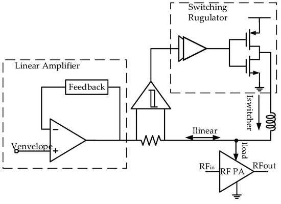
Figure 1.
The system block diagram of the hybrid ET modulator.
Based on the above analysis, this paper presents a hysteresis-controlled 3L-ET modulator and employs a high-speed hysteresis comparator to calibrate the VCF. At the same time, a wideband LA is designed. The structure of this paper is as follows. Section 2 presents the overall structure of the system and makes a brief analysis. Detailed circuit design of each circuit module in Section 3 and Section 4 describes the simulation results of the overall circuit and the final summary is concluded in Section 5.
2. Supply Modulator System Level Design
The three-level hybrid structure used in this paper is shown in Figure 2 and mainly composed of three parts: (1) a linear amplifier; (2) a switching regulator; and (3) a hysteresis control loop. The load resistance RLoad is equivalent to the supply node impedance of a RF PA. In general, linear amplifiers are characterized by high bandwidth and low efficiency, mainly processing the high-frequency part of the input signal and absorbing the noise current generated by the SWR. The switching regulator has the advantage of high efficiency and mainly deals with the DC and low-frequency parts of the input signal. The hysteresis control loop, as a connection between the linear stage and the switching stage, can control the on-off of the switching MOSFET.
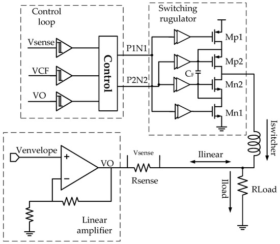
Figure 2.
Block diagram for proposed ET modulator.
The efficiency of the hybrid ET modulator can be expressed as
where Pout is the average output power of the ET modulator and Ploss represents the total power loss. The control loop is mostly logic devices, the power loss is less, so the Ploss is mainly concentrated in the linear stage and the switching stage.
This section will introduce the main blocks of the circuit and analyze the system power consumption.
2.1. Wideband Linear Amplifier
As the bandwidth of the modulated signal increases, the power supply modulator needs to track a higher bandwidth envelope signal, thus requiring more high-frequency output current from LA, which limits overall system efficiency improvements. On the one hand, the bandwidth of the hybrid ET modulator is affected by LA. On the other, the bandwidth of SWR is also gradually increased to reduce the contribution of LA. However, the wideband SWR needs a wideband LA to absorb the high frequency ripple of the switching stage, which makes the LA design more difficult.
The proposed LA has a large unity-gain bandwidth and high driving capability, the overall architecture is shown in Figure 3, including rail-to-rail input stage, buffer stage and class-AB output stage.
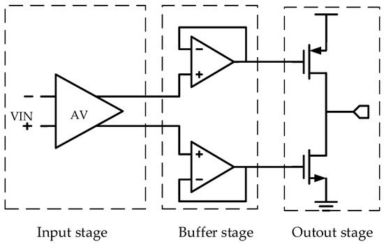
Figure 3.
Simplified schematic of the linear stage.
The power loss of the LA includes static loss and dynamic loss. The dynamic power loss comes from the nMOS and pMOS of the output stage as follows:
where VDD is the supply voltage, Vout is the output voltage at the load, isw is the switch stage current, and iout is the current flowing into the collector/drain of the RF power amplifier. PLA_dy_loss is related to the amplitude probability distribution of the input envelope signal and the peak envelope voltage [25].
The quiescent power loss mainly comes from the quiescent bias current, independent of the output power. Its reduction relies on the design of low-power circuits. In order to improve the driving ability of the LA and reduce the quiescent current as much as possible, a voltage follower is used in this paper. The proposed voltage follower can effectively reduce the output impedance, the specific implementation method is discussed in next section.
2.2. High Efficiency Switching Modulator
The switching regulator employs two pairs of complementary switching transistors as shown in Figure 2. The voltage at the VSW node is 0 to VDD/2 or VDD/2 to VDD, under the ideal conditions, the voltage range across the transistor is maintained at VDD/2. Therefore 3L-SWR can use thin gate-oxide transistors with lower parasitic and lower on-resistance. Compared with the standard two-level buck converter, this converter can reduce the inductor current ripple to 1/4 and the output voltage ripple to 1/8, thus achieving lower switching losses [26].
The power losses in the switching stage include conduction losses and switching losses. Assuming that under the same voltage, the relationship between 3L- switching loss and 2L- switching loss is expressed in [24]
where CP3L and CP2L are the parasitic capacitors of the transistors in 3L-SWR and 2L-SWR, respectively. VSW3L is the switching voltage and fSW3L is the switching frequency of a parasitic capacitor in the 3L-SWR, VSW2L and fSW2L correspond to the parameters in the 2L-SWR. The flying capacitor has parasitic capacitor CFP, as given in [25]. The relationship between CFP and CF is , therefore the switching loss is related to the size of the capacitor CF.
The conduction loss and ripple loss are caused by the on-resistance of pMOS and nMOS. The ratio of conduction loss and ripple loss of the 3L-SW and 2L-SW is given as
where Ron3L and Ron2L are the on-resistance of the single device in 3L-SWR and 2L-SWR, respectively. IL3L and IL2L represent the average inductor currents for 3L-SWR and 2L-SWR, assuming they are equal. Ir is the ratio of the inductor current ripple to the average inductor current, while Ir3L is four times smaller than Ir2L at the same inductance L and the same fSW as shown in [19]. In Equation (6), the ratio can be less than one. If the inductor current ripple is very small, Pcon3L/Pcon2L is only related to the on-resistance, so the 3L-buck converter using thin gate oxide transistors has an advantage over the 2L-buck converter.
Therefore, a 3L-SWR is used to ease the design difficulty of the LA for wideband applications. The detailed circuit design is analyzed in Section 3.
3. Circuit Design
3.1. Linear Amplifier
This section describes a class-AB linear amplifier with rail-to-rail input and output ranges. Figure 4 shows the detailed circuit design of LA. It is worth noting that a source follower (SF) is adopted as a buffer to reduce the output impedance and improve driving capability.
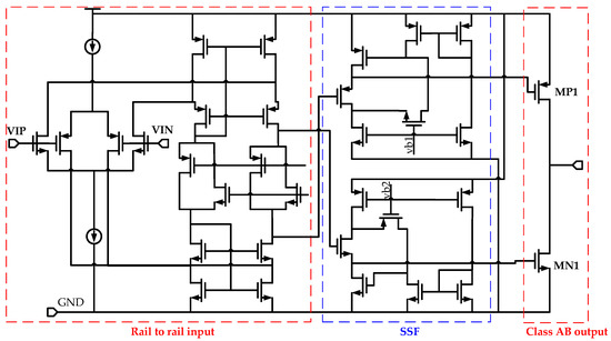
Figure 4.
Detailed circuit of the LA.
The input stage operates in parallel with pMOS and nMOS differential input pairs, enabling the input common-mode range to reach both rails of the supply voltage. To achieve this, it is necessary to ensure that the input-stage transconductance () remains constant over the entire common-mode range. In this structure, the constant transconductance is achieved by using tail current compensation [27]. The class AB output stage can output large current, and has a certain ability to supply power for the load while providing low output impedance.
The output stage is designed to be a common source amplifier to provide high current driving capability. The buffer stage includes two source followers to reduce the output impedance of the circuit. Figure 5a shows a conventional source follower (CSF) [28], the output impedance is approximately . However, the CSF only reduces the output impedance to a certain extent, and it is not suitable for the case if the load is small. Therefore, this paper employs a super source follower (SSF) with feedback loop, as shown in Figure 5b. In this circuit, the feedback loop composed of MNF, MND, and MPB. This loop controls the output transistors MP1 and MN1. The current Ib1 is greater than the current Ib2. Assuming that all transistors are in saturation region, then the current difference between Ib1 and Ib2 flows through the input transistor MNF to the drive transistor MND.
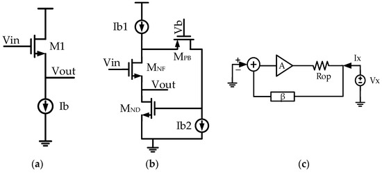
Figure 5.
The block diagram of source followers: (a) conventional source follower; (b) super source follower; and (c) output impedance calculation circuit of the SSF.
Using the classical feedback theory to calculate the output impedance of the SSF, it can be expressed as in Equation (7). Rop is the open-loop output impedance, Aβ is the loop gain. The output impedance of SSF is given by Equation (8).
where gmF is the transconductance of MNF, gmD is the transconductance of MND, and ro2 is the output impedance of current source Ib2.
The output impedance of the LA is simulated, and Figure 6a shows the output impedance versus frequency for different common-mode (CM) input voltages. The frequency response of the LA is shown in Figure 6b, which shows the amplitude and phase margin of the amplifier in open-loop condition. It can be seen that the DC gain is 78 dB, with a phase margin of 45 degrees and the unit gain-bandwidth of 171 MHz. Figure 7 shows the transient simulation results, which verifies that the LA in this paper can amplify the 100 MHz envelope signal well.
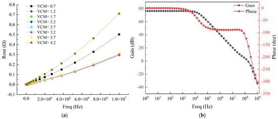
Figure 6.
The AC simulation of the LA: (a) output Impedance of the LA at different CM voltages; (b) the linear amplifier frequency response simulation.
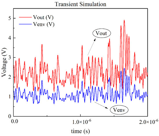
Figure 7.
The transient simulation result of the LA.
3.2. Three-Level Switching Stage
The switching stage of three-level structure buck converter with two pairs of complementary power devices is shown in Figure 8. The drive capability of the logic signal transmitted by the control loop to 3L-SWR is relatively weak, and the size of the power device is usually large, so the buffer stage is needed to improve the driving capability of the control logic signal. Another function of the buffer stage is to prevent the power devices from being turned on at the same time to cause shooting-through phenomenon.
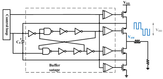
Figure 8.
Block diagram of 3L- SWR.
The PWM waveform output by the control loop is responsible for the turn-on or turn-off of the switching device, and the specific implementation is shown with four operation states in Figure 9. Each state has two transistors on. The four situations of the control loop output are shown in Table 1, where high and low represent VDD and 0 V, respectively.
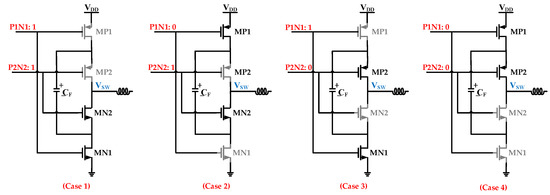
Figure 9.
The four situations of VSW correspond to case 1–4, respectively.

Table 1.
States of the power transistors.
Case 1, when the control loop output sets P1N1 and P2N2 to logic high, MP1 and MP2 are turned off, MN1 and MN2 are turned on, the output node VSW is GND. The result is that the inductor current ISW decreases.
Case 2, when the control loop output P1N1 is logic 0 and P2N2 is logic high, turning MP1 and MN2 on, MP2 and MN1 off, the output node VSW is VDD/2, increasing ISW, and the capacitor CF is in a charging state.
Case 3, when P1N1 is logic high and P2N2 is logic low, MP2 and MN1 are turned on, and MP1 and MN2 are turned off. At the same time, the capacitor CF is discharged, the ISW continues to increase, and the output node VSW is VDD/2.
Case 4, when P1N1 and P2N2 are both logic low, MP1 and MP2 are turned on, MN1 and MN2 are turned off, the output node VSW is VDD, and the ISW continuous output, ensuring that SWR provides more load current. The four states are regarded as a cycle, and the VCF is stabilized around VDD/2 under the action of the control loop.
As described in Section 2.2, the power loss of 3L-SWR is related to parasitic capacitor and on-resistance, and the loss can be minimized by choosing the appropriate capacitor CF and the size of MP and MN. Generally, there are three types of capacitors: metal-insulator-metal (MIM) capacitors, metal-oxide-metal (MOM) capacitors, and MOS capacitors. Large capacitors increase losses and take up chip area. According to the capacitor density, parasitic capacitor percentage and linearity of the capacitor, nMOS capacitors are more suitable, as discussed in [29]. In order to make the voltage variation range of the capacitors smaller, nMOS capacitor CF is selected as 10 nF.
The buffer stage in Figure 8 consists of a chain of inverters, which gradually increase the size and slowly increase the driving capability without wasting too much power loss.
3.3. Control Loop
The logic control circuit connects the linear stage and the switching stage. Through the adjustment of the control circuit, the output current of the LA and SWR is reasonably arranged to maximize the efficiency. The control loop in this paper consists of high-speed hysteresis comparators and logic gate circuits, as shown in Figure 10. The output voltage VO_LA of LA determines which path is used (0 < VO_LA < VDD/2 selects the logic path Ctrl-A, VDD/2 < VO_LA < VDD selects the path Ctrl-B). The current detection resistor RSEN connects the LA and the output terminal, and the voltage of RSEN is Vsense. The simplified representation is shown in Table 2 (the Result column corresponds to Table 1), and the control logic analysis is as follows:
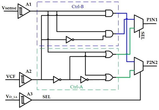
Figure 10.
Circuit structure of the hysteretic control loop.
Table 2.
Operation of the control loop.
- Ctrl-A: When ISW > IL, ILA absorbs excess current, the sinking LA current increases, the output of the A1 comparator is high, and the output of P1N1 and P2N2 is high, resulting in the decrease in ISW and ILA. Due to the decrease in ISW, the sourcing current of ILA increases, and the output of A1 is low. At this time, when VCF is lower than VDD/2, the output of A2 comparator is high, resulting in P1N1 being low and P2N2 being high, increasing ISW. When VCF is higher than VDD/2, the A2 comparator output is low, resulting in P1N1 high and P2N2 low, which also increases ISW.
- Ctrl-B: the sourcing current of ILA increases, the output of the A1 comparator is low, and the output of P1N1 and P2N2 is low, increasing the ISW. If ISW is higher than the load current IL, ILA will absorb the excess current. Like ctrl-A, it repeats the above operation.
Summarizing the above analysis, if the sinking LA current increases, the output of the A1 is high, P1N1 and P2N2 are not in low state at the same time, the corresponding VSW will not be VDD. Similarly, if the sourcing LA current increases, the output of the A1 is low, P1N1 and P2N2 are not high at the same time, the VSW will not be GND. Figure 11 is the simulation result of the control circuit, which verifies the above analysis.
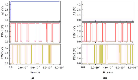
Figure 11.
The logic results of control loop: (a) A1 output is high; (b) A1 output is low.
The control loop employs high-speed hysteretic comparators (Figure 10). This comparator is different from ordinary comparators in that it adopts a positive feedback loop as shown in Figure 12, which is composed of transistors M1-4. M3 and M4 have the same W/L, and M1 and M2 are the same. The hysteresis width H is related to β = (W/L) 3,4/(W/L)1,2, and H is changed by adjusting β. In this design, the hysteresis width of comparators A1, A2, and A3 are 10 mV, 20 mV, and 50 mV, respectively.
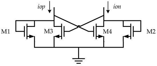
Figure 12.
Positive feedback loop of hysteretic comparator.
4. Simulation Results
In this paper, the envelope tracking modulator is designed with 180 nm process. Figure 13 shows the layout of the ET supply modulator. The operation conditions of the modulator are that the supply voltage is 5 V, the equivalent load of PA is 6 ohms, and an on-chip integrated capacitor of 10 nF. In addition, a 1.1 uH off-chip inductor is used for simulation.
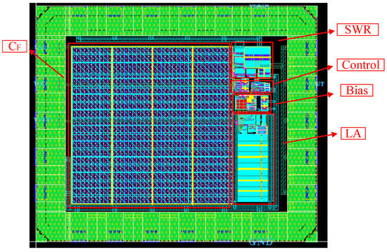
Figure 13.
Layout of the ET supply modulator.
The transient simulation results of the ET modulator are shown in Figure 14. The input signal comes from 5G NR 100 MHz envelope signal with maximum PAPR 7.5 dB (after the PAPR reduction process). Figure 14a shows the simulation waveform. From top to bottom, it shows the input envelope waveform, output waveform, and 3L-SWR switching node voltage. The total output current, SWR output current, and LA output current are shown in Figure 14b. Current transient simulation results show that the total output current is equal to the sum of the ILA and the ISWR. When the ISWR is greater than the ILoad, the LA sinks the excess current. On the contrary, when the ISWR is less than the ILoad, the LA supplies the remaining current. This ensures that most of the ILoad is provided by the SWR, further improving the overall efficiency of the system.
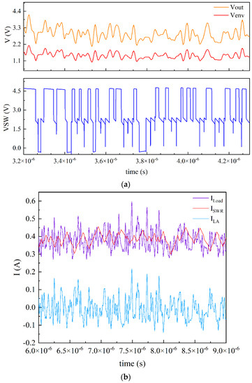
Figure 14.
Transient simulation result of ET modulator for 100 MHz input signal: (a) input and output waveforms, 3L operation; (b) LA output current ILA, SWR output current ISWR, total output current ILoad.
Figure 15 shows the curve of the overall efficiency and output power of the ET modulator with the change of load. When the load resistance is 10 ohms, the efficiency reaches the maximum close to 85%, and the output power is 0.92 W.
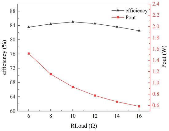
Figure 15.
Simulation curve of output power and efficiency versus load resistance.
Table 3 summarizes the performance of the envelope amplifier designed in this work and compares it with some previous work. The bandwidth of the envelope signal in this paper is 100 MHz; under this condition, the modulator has higher efficiency and output power. The output voltage range of the modulator is 0.3 V–4.6 V. The higher output voltage can provide a large power supply voltage to PA, which is suitable for a broad application. Thanks to the hysteretic comparator, the flying capacitor does not require an additional calibration circuit, which reduces the difficulty of circuit design.
Table 3.
Performance comparison with the prior arts.
5. Conclusions
A hybrid envelope tracking supply modulator consisting of a class-AB linear amplifier, a three-level switching regulator, and a high-speed hysteresis control loop was presented in this paper. The proposed super source follower enables the linear amplifier to have a low output impedance at a very high frequency. Meanwhile, the hysteresis control method improves the loop response speed and the bandwidth of the switching regulator. The simulation results show that the modulator can track the 100 MHz envelope signal well with 85% peak efficiency. In addition, the modulator has a maximum output power of 1.5 W at the supply voltage of 5 V.
Author Contributions
Conceptualization, Y.L.; funding acquisition, Y.L., X.Q.; methodology, K.Y., Y.L., C.C., X.C.; project administration, X.Q., B.X.; resources, X.Q.; software, C.C., B.X., M.H.; supervision, Y.L., X.C., B.X.; validation, X.C., M.H.; writing—original draft, K.Y.; writing—review and editing, C.C. All authors have read and agreed to the published version of the manuscript.
Funding
This research is supported by the National Natural Science Foundation of China under the grant No. 61971414 and Henan Province Key R&D and Promotion Project (Science and Technology Research) No. 212102210027 and Zhengzhou Zhongke Institute of Integrated Circuit and System Application Research Dean Fund No. ZK2005BN003.
Institutional Review Board Statement
Not applicable.
Informed Consent Statement
Not applicable.
Conflicts of Interest
The authors declare no conflict of interest.
References
- Jiang, T.; Wu, Y. An Overview: Peak-to-Average Power Ratio Reduction Techniques for OFDM Signals. IEEE Trans. Broadcast. 2008, 54, 257–268. [Google Scholar] [CrossRef]
- Lavrador, P.M.; Cunha, T.R.; Cabral, P.M.; Pedro, J. The Linearity-Efficiency Compromise. IEEE Microw. Mag. 2010, 11, 44–58. [Google Scholar] [CrossRef]
- He, H.; Kang, Y.; Ge, T.; Guo, L.; Chang, J.S. A 2.5-W 40-MHz-Bandwidth Hybrid Supply Modulator With 91% Peak Efficiency, 3-V Output Swing, and 4-mV Output Ripple at 3.6-V Supply. IEEE Trans. Power Electron. 2019, 34, 712–723. [Google Scholar] [CrossRef]
- Wu, P.Y.; Mok, P.K.T. A Two-Phase Switching Hybrid Supply Modulator for RF Power Amplifiers with 9% Efficiency Improvement. IEEE J. Solid-State Circuits 2010, 45, 2543–2556. [Google Scholar] [CrossRef]
- Jing, Y.; Bakkaloglu, B. A High Slew-Rate Adaptive Biasing Hybrid Envelope Tracking Supply Modulator for LTE Applications. IEEE Trans. Microw. Theory Tech. 2017, 65, 3245–3256. [Google Scholar] [CrossRef]
- Park, B.; Kim, D.; Kim, S.; Cho, Y.; Kim, J.; Kang, D.; Jin, S.; Moon, A.; Kim, B. High-Performance CMOS Power Amplifier with Improved Envelope Tracking Supply Modulator. IEEE Trans. Microw. Theory Tech. 2016, 64, 798–809. [Google Scholar] [CrossRef]
- Jin, S.; Park, B.; Moon, K.; Kim, J.; Kwon, M.; Kim, D.; Kim, B. A Highly Efficient CMOS Envelope Tracking Power Amplifier Using All Bias Node Controls. IEEE Microw. Wirel. Compon. Lett. 2015, 25, 517–519. [Google Scholar] [CrossRef]
- Hanington, G.; Chen, P.-F.; Asbeck, P.M.; Larson, L.E. High-efficiency power amplifier using dynamic power-supply voltage for CDMA applications. IEEE Trans. Microw. Theory Tech. 1999, 47, 1471–1476. [Google Scholar] [CrossRef]
- Sahu, B.; Rincon-Mora, G.A. A high-efficiency linear RF power amplifier with a power-tracking dynamically adaptive buck-boost supply. IEEE Trans. Microw. Theory Tech. 2004, 52, 112–120. [Google Scholar] [CrossRef]
- Chu, W.; Bakkaloglu, B.; Kiaei, S. A 10 MHz Bandwidth, 2 mV Ripple PA Regulator for CDMA Transmitters. IEEE J. Solid-State Circuits 2008, 43, 2809–2819. [Google Scholar] [CrossRef]
- Lin, Y.-C.; Chen, Y.-J.E. A CMOS Envelope Tracking Supply Converter for RF Power Amplifiers of 5G NR Mobile Terminals. IEEE Trans. Power Electron. 2021, 36, 6814–6823. [Google Scholar] [CrossRef]
- Kim, D.; Kang, D.; Kim, J.; Cho, Y.; Kim, B. Highly Efficient Dual-Switch Hybrid Switching Supply Modulator for Envelope Tracking Power Amplifier. IEEE Microw. Wirel. Compon. Lett. 2012, 22, 285–287. [Google Scholar] [CrossRef]
- Hassan, M.; Asbeck, P.M.; Larson, L.E. A CMOS dual-switching power-supply modulator with 8% efficiency improvement for 20 MHz LTE Envelope Tracking RF power amplifiers. In Proceedings of the 2013 IEEE International Solid-State Circuits Conference Digest of Technical Papers, San Francisco, CA, USA, 17–21 February 2013; pp. 366–367. [Google Scholar]
- Paek, J.-S.; Kim, D.; Bang, J.-S.; Baek, J.; Choi, J.; Nomiyama, T.; Han, J.; Choo, Y.; Youn, Y.; Park, E.; et al. An 88%-Efficiency Supply Modulator Achieving 1.08 μs/V Fast Transition and 100 MHz Envelope-Tracking Bandwidth for 5G New Radio RF Power Amplifier. In Proceedings of the 2019 IEEE International Solid-State Circuits Conference—(ISSCC), San Francisco, CA, USA, 17–21 February 2019; pp. 238–240. [Google Scholar]
- Ho, C.-Y.; Lin, S.-M.; Meng, C.-H.; Hong, H.-P.; Yan, S.-H.; Kuo, T.-H.; Peng, C.-S.; Hsiao, C.-H.; Chen, H.-H.; Sung, D.-W.; et al. An 87.1% efficiency RF-PA envelope-tracking modulator for 80MHz LTE-Advanced transmitter and 31dBm PA output power for HPUE in 0.153 μm CMOS. In Proceedings of the 2018 IEEE International Solid—State Circuits Conference—(ISSCC), San Francisco, CA, USA, 11–15 February 2018; pp. 432–434. [Google Scholar]
- Paek, J.-S.; Youn, Y.-S.; Choi, J.-H.; Kim, D.; Jung, J.-H.; Choo, Y.; Lee, S.-J.; Lee, S.-C.; Cho, T.; Kang, I. An RF-PA supply modulator achieving 83% efficiency and −136 dBm/Hz noise for LTE-40 MHz and GSM 35 dBm applications. In Proceedings of the 2016 IEEE International Solid-State Circuits Conference (ISSCC), San Francisco, CA, USA, 31 January–4 February 2016; pp. 354–355. [Google Scholar]
- Riehl, P.; Fowers, P.; Hong, H.-P.; Ashburn, M. An AC-coupled hybrid envelope modulator for HSUPA transmitters with 80% modulator efficiency. In Proceedings of the 2013 IEEE International Solid-State Circuits Conference Digest of Technical Papers, San Francisco, CA, USA, 17–21 February 2013; pp. 364–365. [Google Scholar]
- Meynard, T.A.; Foch, H. Multi-level conversion: High voltage choppers and voltage-source inverters. In Proceedings of the PESC ‘92 Record. In Proceedings of the 23rd Annual IEEE Power Electronics Specialists Conference, Toledo, Spain, 29 June–3 July 1992; Volume 1, pp. 397–403. [Google Scholar]
- Yousefzadeh, V.; Alarcon, E.; Maksimovic, D. Three-level buck converter for envelope tracking applications. IEEE Trans. Power Electron. 2006, 21, 549–552. [Google Scholar] [CrossRef]
- Kim, W.; Brooks, D.; Wei, G.-Y. A Fully-Integrated 3-Level DC-DC Converter for Nanosecond-Scale DVFS. IEEE J. Solid-State Circuits 2012, 47, 206–219. [Google Scholar] [CrossRef]
- Liu, X.; Huang, C.; Mok, P.K.T. A High-Frequency Three-Level Buck Converter with Real-Time Calibration and Wide Output Range for Fast-DVS. IEEE J. Solid-State Circuits 2018, 53, 582–595. [Google Scholar] [CrossRef]
- Mahmoudidaryan, P.; Mandal, D.; Bakkaloglu, B.; Kiaei, S. A 91%-Efficiency Envelope-Tracking Modulator Using Hysteresis-Controlled Three-Level Switching Regulator and Slew-Rate-Enhanced Linear Amplifier for LTE-80MHz Applications. In Proceedings of the 2019 IEEE International Solid-State Circuits Conference—(ISSCC), San Francisco, CA, USA, 17–21 February 2019; pp. 428–430. [Google Scholar]
- Tan, M.; Ki, W. A 100 MHz Hybrid Supply Modulator with Ripple-Current-Based PWM Control. IEEE J. Solid-State Circuits 2017, 52, 569–578. [Google Scholar] [CrossRef]
- Mahmoudidaryan, P.; Mandal, D.; Bakkaloglu, B.; Kiaei, S. Wideband Hybrid Envelope Tracking Modulator with Hysteretic-Controlled Three-Level Switching Converter and Slew-Rate Enhanced Linear Amplifier. IEEE J. Solid-State Circuits 2019, 54, 3336–3347. [Google Scholar] [CrossRef]
- Wang, F.; Kimball, D.F.; Popp, J.D.; Yang, A.H.; Lie, D.Y.; Asbeck, P.M.; Larson, L.E. An Improved Power-Added Efficiency 19-dBm Hybrid Envelope Elimination and Restoration Power Amplifier for 802.11g WLAN Applications. IEEE Trans. Microw. Theory Tech. 2006, 54, 4086–4099. [Google Scholar] [CrossRef]
- Meynard, T.A.; Foch, H.; Thomas, P.; Courault, J.; Jakob, R.; Nahrstaedt, M. Multicell converters: Basic concepts and industry applications. IEEE Trans. Ind. Electron. 2002, 49, 955–964. [Google Scholar] [CrossRef]
- Hogervorst, R.; Tero, J.P.; Eschauzier, R.G.H.; Huijsing, J.H. A compact power-efficient 3 V CMOS rail-to-rail input/output operational amplifier for VLSI cell libraries. In Proceedings of the IEEE International Solid-State Circuits Conference—ISSCC ‘94, San Francisco, CA, USA, 16–18 February 1994; pp. 244–245. [Google Scholar]
- Gray, P.R.; Hurst, P.J.; Lewis, S.H.; Meyer, R.G. Analysis and Design of Analog Integrated Circuits, 5th ed.; John Wiley & Sons Inc.: Hoboken, NJ, USA, 2009; pp. 212–214. [Google Scholar]
- Liu, X.; Mok, P.K.T.; Jiang, J.; Ki, W.-H. Analysis and Design Considerations of Integrated 3-Level Buck Converters. IEEE Trans. Circuits Syst. I Regul. Pap. 2016, 63, 671–682. [Google Scholar] [CrossRef]


Publisher’s Note: MDPI stays neutral with regard to jurisdictional claims in published maps and institutional affiliations. |
© 2022 by the authors. Licensee MDPI, Basel, Switzerland. This article is an open access article distributed under the terms and conditions of the Creative Commons Attribution (CC BY) license (https://creativecommons.org/licenses/by/4.0/).