1. Introduction
Due to its flexibility, active thermography is used in many fields of applications [
1]. Pulsed, step-heating, and lock-in thermography are among the most commonly applied techniques. A wide range of post-processing, image correction and analysis procedures have been developed [
2,
3,
4]. All methods of active thermography have in common that they require an external excitation source. Depending on the nature of the object and the aim of the investigation, an appropriate source has to be chosen. Excitation sources based on the principles of inductive, microwave, resistive, mechanical, and convective heating have been used [
5]. However, the most commonly used heat sources are based on optical excitation. The sources can be lasers in the form of spot lasers, line lasers, or laser arrays, while for short and powerful excitation, flash lamps are suitable. In other cases, projectors or halogen lamps in combination with shutters are sufficient. As an alternative, LEDs can be used, which is described in the following.
To achieve good results in non-destructive testing, a well-designed excitation source is of central importance, a range of performance criteria are discussed in the community [
1]. First, the excitation should have a high degree of spatial homogeneity or at least a well-known radiant intensity distribution. In addition, the source has to be powerful enough to enable thermal measurements with sufficient signal-to-noise ratio. To obtain robust results, a good repeatability is necessary, both over the long and the short term. In case of optical excitation, this includes effects such as lamp aging or self-heating of the lamp during operation. Furthermore, the signal shape of the excitation is important. This includes the pulse duration for flash excitation, the steepness of the step for step excitation, or the harmonic distortion for lock-in applications. For lock-in applications in particular, the response characteristics of the source are relevant, i.e., amplitude and phase response as a function of the lock-in frequency. For optical excitation, an overlap of the emission spectrum with the infrared detection range should be avoided.
Lock-in thermography is a technique, which relies on a stable periodic signal to create amplitude and phase images of thermal waves. The technique is typically used for defect detection [
6,
7] or the measurement of material parameters such as the thermal diffusivity, see, e.g., [
8,
9,
10]. Layer thickness measurements are also possible, see, e.g., [
11,
12,
13].
Over time, lasers have become more and more attractive as excitation sources for lock-in thermography. They are used in a variety of different setups. An application example of a spot laser in modulated continuous wave mode is given by An et al. [
14]. In their work, the authors highlight the advantages of laser lock-in thermography such as long-distance energy transmission and highly controllable emission. The importance of being able to modulate the excitation source arbitrarily is highlighted by Kopera et al. [
15]. They use the arbitrary modulation capability of a diode laser for multiplexed lock-in frequencies to reduce the temperature drift in a lock-in measurement due to DC components. The spatial focus is one of the main advantages of laser lock-in thermography. Spot lasers enable for thermal diffusivity measurements via the slope method [
16]. In defect detection, the small beam width and high power of lasers is utilized in laser scanning for high spatial resolution [
17,
18]. Spatially more extended excitation is available from vertical-cavity surface-emitting lasers (VCSEL) [
19]. Using VCSELs, highly controllable excitation up to several kilowatts is available. Other sources that have been investigated include LCD projectors [
20] or laser-coupled digital micromirror devices (DMD) [
21].
A valuable comparison of common excitation sources for lock-in thermography is given by Ziegler et al. [
22]. In their work, they compare halogen lamps, LEDs, and VCSELs in terms of modulation bandwidth, spectrum, and irradiance. The work shows the clear advantage of LEDs and VCSELs with respect to frequency stability. The theoretical minimal irradiance, which is necessary to obtain a clear thermographic signal on various types of coated and uncoated metals, is compared on the basis of a set of technical assumptions. The authors conclude that the LED sources are mainly limited by their irradiance compared to VCSEL.
While the disadvantages of halogen lamps are often noted, they offer some distinct advantages over other sources. Halogen lamps are powerful and inexpensive sources, which are easy to obtain. They can be easily integrated into a setup without the need of expensive periphery. Moreover, they can be safely operated, in particular in comparison with high-power lasers. Yet, the maximum modulation frequency as well as the dynamic range are limited by the high thermal inertia of halogen lamps. In comparison, they feature low spatial resolution and often exhibit inhomogeneous excitation. The focusing and modulation of halogen lamps via optics and shutters is often experimentally tedious. In addition, the emission of halogen lamps has a spectral overlap with the infrared detection range. Powerful halogen lamps often induce a high amount of ambient heating, which potentially causes temperature drifts during the experiment.
On the other end of the price range are powerful laser systems such as DPSS (diode-pumped solid state lasers), gas laser, high-power laser diode bar modules, and VCSEL (vertical-cavity surface-emitting laser). For different laser types and modulation frequencies, various modulation schemes can be applied. This includes the modulation of the driving current of diode laser or diode pumped lasers, the employment of acousto-optic modulators, galvanometers, external shutters, or the use of Q-switched lasers. While this makes the usage of lasers very versatile and customizable, each combination of laser and modulation scheme comes with its own challenges. For example, modulation of a diode laser by modulating its pump current is comparatively easy. However, the nonlinear nature of the laser emission might lead to nonlinear behaviour of the optical output power in the non-equilibrium stage after changing the pump current. As a result, the temporal shape of the optical output power is distorted if not taken into account properly. Nevertheless, lasers offer high optical power with a small étendue, enabling precise shaping of their beams by optical elements. This could be used to generate specific excitation pattern or tightly focused spots. However, damage thresholds have to be taken into account, as high local excitation powers are not be suitable for all samples [
14]. While the experimental challenges of using a laser system are one thing, the safety issues when working with high-power lasers are another. High optical powers and tightly confined beams make thorough enclosure of the experiments a necessity.
A good compromise with respect to price-to-performance ratio is the use of LEDs. While LEDs are not as bright as lasers, the output power can be controlled in a wide range via the driving current. However, the use of a conventional LED-based luminaire is often not practical. This is usually due to the restrictions of the included driver-circuit as well as the limited radiant intensity. A work on LEDs for non-destructive testing by Pickering et al. [
23] uses water-cooled phosphor-based LEDs for long-pulse excitation and lock-in thermography. The paper notes the advantages of LEDs in terms of price, technical complexity, and emission spectrum. However, the paper also notes problems with residual infrared emissions in the camera detection range and heat sink design. Certain monochromatic LEDs, for example in the infrared spectrum (with emission outside the camera detection sensitivity), have increased efficiency and are less temperature sensitive as no phosphor for light conversion is necessary. This allows for a higher operating temperature, higher irradiance and a narrower spectrum. Achieving high irradiances is the main challenge using LED-based excitation sources, which is directly connected to a good thermal management.
In this work, the schematics of an infrared LED-based excitation source as well as its driver circuit are presented in detail. The source includes a digital and analogue input to fully control the LED current and to produce arbitrary output signals. This includes but is not limited to sinusoidal emission. The excitation source is investigated for its amplitude and phase response as well as its thermal and optical properties. A comparison to the performance of a halogen lamp as well as a halogen lamp and mechanical chopper combination is given.
2. Hardware Design
2.1. Housing and Specifications
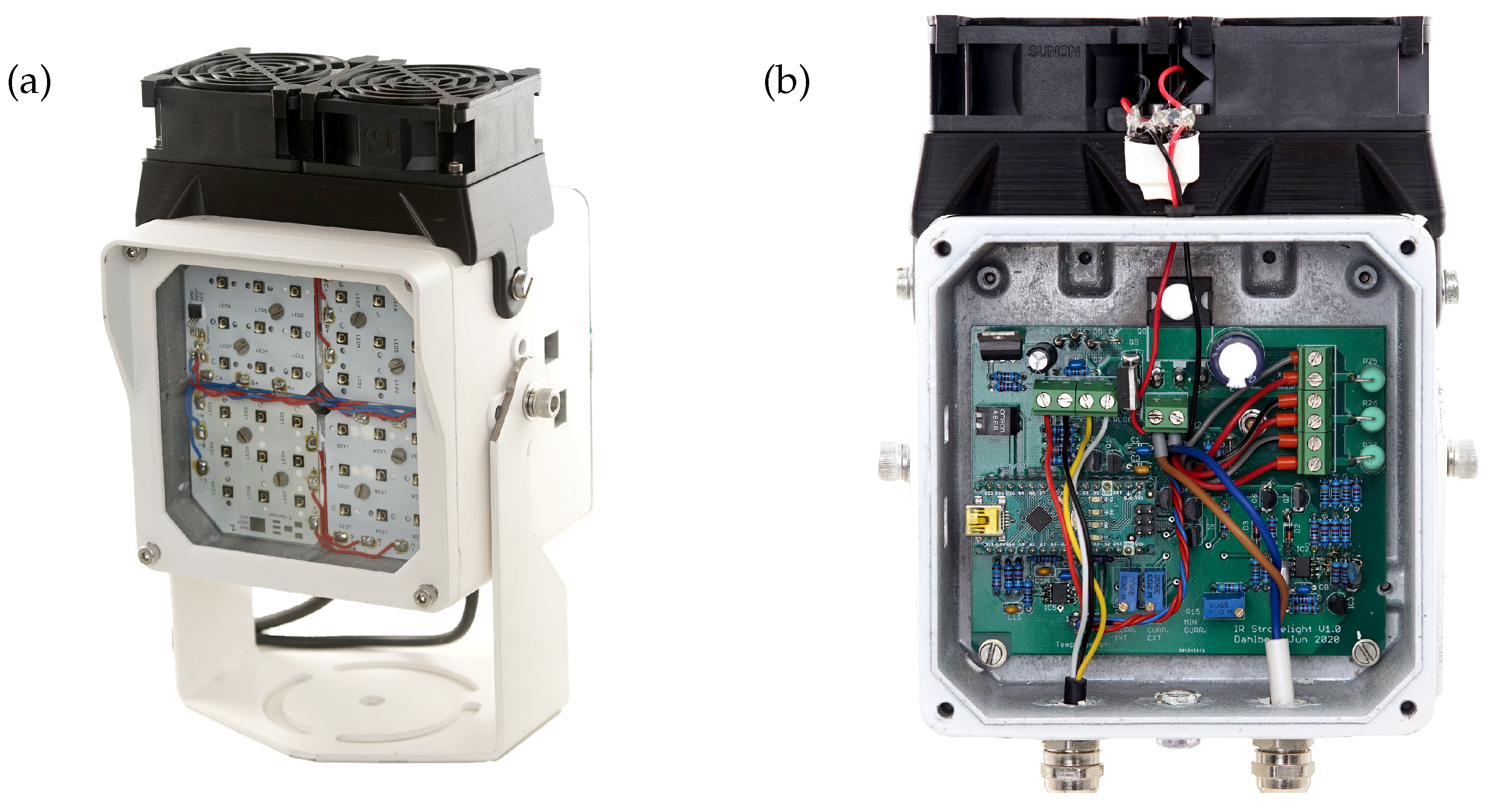
The excitation source described in this work is shown in
Figure 1. On the left, the source is shown from the front, where the array of infrared LEDs is visible. The LEDs are mounted on an aluminium substrate PCB (printed circuit board), which acts as a heat spreader. For the housing, the hull of a commercially available infrared strobe lamp is used. It provides enough space for an LED board with the dimensions
. The necessary control elements are mounted on the back side of the housing, see
Figure 1b.
The housing features a central cooling channel for heat dissipation (
Figure 2). The channel splits the housing into two chambers and offers two surfaces, which are thermally well-connected to the ambient. The front chamber houses the LED boards, which are directly connected to the cooling channel. The back chamber contains the driver circuit and the output transistor bolted to the cooling channel. Thermal compound is pasted between the boards and the faces of the channel to increase the heat transfer coefficient. Running the excitation source for longer periods at full power reveals that passive cooling via the cooling channels in the middle of the housing does not provide sufficient heat dissipation. Therefore, two cooling fans (Sunon MF60252V2-1000U-A99) are installed to provide additional ventilation. The 24 V/ 60 mm fans are connected in series and powered by the same power supply as the LED driver. Parallel to each fan, a 220 μF capacitor is added for current smoothing. A 3D-printed intermediate part builds the transition between the cross-sections of the fans and the cooling channel. With this addition, the temperature of the housing does not exceed 50 °C. To minimize the power dissipation inside the housing, an external switched-mode power supply module is used.
To use the LED excitation source in a wide range of applications, including lock-in and transient measurements, different operating modes are implemented, to control the LED current and the duty cycle. As the control input, a BNC-connector is used, which comprises an analogue and a digital input. The analogue input is used for direct or pulse-width modulation dimming. The digital input allows for switching the output upon a trigger signal. A USB connection is added to allow a remote control via a computer. The excitation source is designed to have a usable frequency range from DC up to 1 kHz to fit a wide range of lock-in applications (
Table 1). Rise and fall time are specified to allow the use of the excitation source in transient thermography applications.
2.2. LEDs and Optics
Placing the LEDs on a 14 mm grid gives space for 36 LEDs inside the housing in a
layout. For the LEDs, infrared LEDs of the type OSLON
® Black SFH4715AS from OSRAM Opto Semiconductors are used [
24]. At a rated forward current of 1 A, this single-emitter LED emits an optical power of
W at a nominal wavelength of 850 nm. Using 36 LEDs, the resulting optical power amounts to 55 W. The spectral bandwidth (full width half maximum) of the LEDs is approximately 30 nm. The half angle of its emission cone (without additional optics) is 40
.
The LED board is divided into four smaller PCBs, each containing 9 LEDs. Electrically, the LEDs are split into 3 strings, each consisting of 12 LEDs. The resulting LED forward current and forward voltage are important specifications for the LED driver circuit (
Table 1). This partitioning of the LED strings allows voltage matching of the LED strings. By swapping individual sub-strings between the total strings, the differences in forward voltage between the strings are minimized.
The OSLON® Black SFH4715AS provides a good compromise between price per unit and optical output power. Alternatively, chip-on-board LEDs could be used as optical emitters. While they offer a higher optical output, typically their emission cones are wider, the use of additional optics is more difficult, and the thermal load is more demanding.
A 14 mm spacing allows the use of conventional LED lenses to narrow the beam angle of the infrared radiation and to increase the radiant intensity. To allow an unobstructed field of view when a sample is investigated from the excitation side, the excitation source has to be at a distance of approximately 30 cm from the sample. Therefore, the beam has to be narrowed down and ideally have a focus point at this distance. For this, LED optics of the type LEDiL LISA2-RS-PIN are added, which have a beam angle (full width half maximum) of 19°. In
Figure 3a, the LED lenses are visible. For some applications, it is useful to concentrate the optical power on a surface area that is smaller than the cross-section of the excitation source. For these cases, a parabolic, 3D-printed reflector is designed, which is attachable to the excitation source, see
Figure 3b. The inside of the reflector is covered with an reflective aluminium adhesive tape.
2.3. Circuit Topology
In this section, a description of the functionality of the driver circuit is given. The circuit diagram of the LED excitation source is shown in
Figure 4. Connections to the controller are indicated as gray labels. The circuit simulation projects in LTspice, the firmware for the Arduino Nano, the STL files for the 3D-printed parts, and schematics for the hardware are included in the
Supplementary Material of this article. The three LED strings are connected in parallel with one common output transistor. Each string has a separate shunt resistor, which also acts as a balancing resistor. To drive the LEDs, a switched topology and a linear topology are considered. The switched topology is based on a hysteretic step-down converter, designed to have a ripple of 300 mA (10% of the maximum current) at a switching frequency of approximately 150 kHz. The linear topology approach directly controls the LED current with the output transistor using a proportional-integral (PI) controller. Both topologies are simulated using the freely available electronic simulation software LTspice
® [
25].
The switched topology shows a rise time of
and a fall time of
, whereas the linear topology shows a rise time of
and a fall time of
. Thus, the switched topology approach does not meet the criteria of
Table 1. In addition, the slow rise time of the switched topology leads to a lower effective duty cycle when the output is pulse-width modulated. This deteriorates the modulation linearity. As the hysteresis controller of the switched topology only oscillates above a threshold of half the ripple current, the LEDs cannot be dimmed at low current values. Due to the better transient performance and linearity, the linear topology approach is chosen over the switched one.
The circuit is powered by an external adjustable switched-mode power supply unit of the type Mean Well HEP-185-36A. The output voltage of the power supply unit can be varied in the range from 33 V to 40 V. The voltage chosen is 4 V above the forward voltage of the LEDs, leaving enough regulation reserve for the output transistor. When choosing the supply voltage such that it is only 4 V over the LED forward voltage, the power dissipation of the output transistor is 12 W, which is low compared to the electric power of the LEDs of 101 W. If the voltage reserve is set lower, the control loop tends to oscillate. A relative voltage of 4 V is chosen as a compromise between control stability and power dissipation. The 15 V supply consists of a 7815TV linear regulator, which is connected to the LED supply voltage. Z-diodes are added to the input of the linear regulator to meet its input voltage limit of 35 V.
The currents through the LED strings are measured with individual shunts. The shunt voltage is referenced to ground by the averaging differential amplifier formed by the right TLV272 operational amplifier. As this amplifier operates below unity gain, capacitors are added in the feedback network to avoid oscillations. The TL431 adjustable voltage reference IC on the right offsets the output of the differential amplifier by V and thus avoids saturation of the amplifier. The 168 resistors are composed of a 100 and a 68 resistor each. The number of LED strings can be varied to accommodate a different number of LEDs. The value of the 168 resistors then has to be modified to maintain an equivalent parallel resistance of 56 of the resistors connected to the LED strings. For example, the value of these resistors has to be changed to 112 when two strings are in use. The left TLV272 operational amplifier forms a PI current controller, which controls the IRFP244N output transistor via a discrete gate driver. When a larger number of LEDs is used, the current of all strings can be raised up to 8 A. This maximum permissive current is limited by the power dissipation of the output transistor. The forward voltage of an LED string can be as high as 55 V, which is in turn limited by the maximum rating of the components in the 15 V supply. This means that LED arrays with an electrical power of up to 440 W can be driven by this circuit.
With the two 2N7000 MOSFETs on the top left, either an internal or an external reference value can be fed to the current controller. To minimize the effects of charge injection in these MOSFETs, relatively high values are used for the gate resistors. They are controlled by an Arduino Nano microcontroller (not shown in
Figure 4). The two upper trimming resistors allow to adjust the maximum LED current. They are designed so that the LED current through one string can be adjusted in the range between
A and 1 A with an input voltage of either
V or 5 V at the external input or 10 V at the internal input. The current range of
A to 1 A allows the use of alternative LEDs with a maximum forward current of down to
A.
To allow a fast switching of the output, the lower 2N7000 can short the reference voltage to ground level. This switching cannot be slowed down by large value gate resistors, therefore the gate charge injection has to be compensated by an inverted charge injection. This is done by the cascode amplifier formed by the two BC547 transistors on the bottom left. A common emitter inverter circuit was also investigated, but it has been proven to be too slow to effectively compensate the injected pulse when switching.
The Arduino Nano microcontroller does not provide a direct analogue output. Instead, it provides a pulse-width modulation (PWM) functionality, which is used to modulate the LEDs. By directly manipulating the corresponding registers of the ATMEGA328P microcontroller, the PWM frequency can be set to a value of
kHz, which is an order of magnitude above the frame rate of common infrared cameras. To obtain an analogue value from the PWM signal, a second order Bessel lowpass filter with a cutoff frequency of 100 Hz is applied. This functionality is provided by a third operational amplifier (not shown in
Figure 4). The filter has a DC amplification factor of two, resulting in a higher voltage range of up to 10 V. The goal of this measure is to minimize the relative influence of the residual output voltage when the output is pulled to ground level.
As the excitation source has a high optical output power, an interlock is added for connection to a safety switch. If the switch is opened, the PHP79NQ08LT MOSFET switches off the output. By feeding the interlock state to the controller, the excitation source can be programmed in a way that the output does not turn on when the switch closes again, but has to be enabled again by a remote command.
2.4. Operating Modes
To use the excitation source for lock-in setups as well as DC and transient output powers, using the digital or analogue input, four operation modes are implemented in the microcontroller. The operating modes are illustrated in
Figure 5. In Mode A, a suitable analogue input is fed directly to the current controller. To adjust the average power level of the LED current,
, the duty cycle is adjusted. Mode B utilizes the microcontroller to set the LED current,
, via pulse-width modulation. The current value during the pulses is adjusted by a serial command. In Mode C, the input triggers an interrupt at a falling or rising edge, which switches the output on or off. Both peak current and duty cycle are adjustable via serial commands. This operating mode is useful when the input signal is sinusoidal and the output signal should be rectangular or when the input signal has significant overshoot and cannot be fed directly to the output. When Mode D is selected, the analogue input signal is ignored. This mode is used when the excitation source is controlled digitally. The operating mode is set either by a dual in-line package (DIP) switch connected to the microcontroller or by corresponding serial commands.
The PCB was designed so that the traces through which the LED current flows are contained in the top right-hand corner, spanning an area as small as possible, minimizing the traces’ inductance. They are spaced apart from the circuit elements dealing with analogue signals on the bottom part of the PCB to avoid interference. Both the DIP switch and the USB port of the microcontroller are placed on one left-hand side.
3. Experimental Specifications
3.1. Thermal Characterization
Infrared thermography is used to estimate the maximum junction temperature of the LEDs, which are the most temperature-sensitive elements of the device. Having operated the lamp continuously for 90 min with
, a thermographic image of the LED board is recorded (
Figure 6). The infrared thermography system used is based on a cooled indium antimonide focal plane array snapshot detector to detect radiation between
m and
m (Infratec ImageIR 8380S). In full frame mode, a resolution of
is possible. As the optics of the LEDs are assumed to have an emission coefficient larger than 0.9, no emissivity correction is necessary.
For a proper estimate of the junction temperature, the thermal resistance between junction and primary optic is taken into account. The maximum surface temperature at point 1 is 82.9 °C, while it is 78.9 °C at point 2. The temperature rise in the junction is assumed to be up to 10% higher than the hottest surface temperature. Under these assumptions, the junction temperatures at points 1 and 2 are estimated to be 91.2 °C and 86.8 °C, respectively. Both values lie well below the specified maximum junction temperature of 145 °C [
24].
The thermal resistance (junction to ambient) is defined as the temperature difference,
, to ambient temperature divided by the magnitude of the applied power,
P, i.e.,
To obtain the thermal resistance, it is necessary to estimate the power step,
P, per LED. For the thermographic image, as shown in
Figure 6, the LEDs are operated with
, the average forward voltage is
for each LED. According to the datasheet, the typical emitted optical power at
A is
. Thus, the heating power,
, amounts for each LED to
At an ambient temperature of 20 °C, the junction-to-ambient thermal resistances amount to
for points 1 and 2, respectively.
3.2. Radiant Intensity Distribution
To measure the radiant intensity in the far field, a robot goniophotometer (opsira robogonio mrg-6) in combination with an optical powermeter (Thorlabs PM100D with power sensor S121C) is used. For the experiments, the LED output power is set to 90% of the maximum power. The C0–C180 and C90–C270 planes of the angular distribution of the radiant intensity with and without focusing optic are shown in the top row of
Figure 7. The intensity distribution shows a radial symmetry, i.e., no significant differences between the two C-planes are visible.
Without focusing optic, the maximum of the radiant intensity distribution is 24
/
. This is less than expected from the summation of the typical maximum intensity of
per LED according to the datasheet [
24], i.e., a maximum intensity of
is expected for the total LED board. The observed difference of more than 5
is caused by the use of LEDs belonging to a lower grade batch with a maximum radiant intensity of 780 mW/
only. This leads to a maximum intensity of
, which is very close to the measured value of 24
/
. In addition to the fact that LEDs of lower grade are used, shadowing effects are present at angles larger than 25
(
Figure 7a top). This also contributes to the slightly reduced experimental value. The integrated optical power of the board amounts to 32
.
In contrast to the LED source without optic, the source with focusing optic shows a significantly narrower distribution with a maximum of the radiant intensity of 72
/
(
Figure 7b top) and a total optical power of 24
. The decrease in total optical power of 8
is attributed to losses by the optic. The bottom row of
Figure 7 shows the irradiance on an area of
m ×
m at a distance of
. The maximum irradiance generated by the source without additional optic is 96 W/m
2 whereas the addition of the optic increases this value to 275 W/m
2.
3.3. Signal Response Characteristic
The infrared LED lamp is compared to two other modulated sources: an electrically modulated 150 W halogen reflector lamp of the type 64635 HLX and the same halogen lamp modulated by a Thorlabs MC2000-EC mechanical chopper. The signal of the LED excitation source and the chopper setup are measured with a BPW34 photodiode. The diode is driven with 9 V in reverse bias and connected to the input of the lock-in amplifier. Amplitude and phase are measured with an SR860 lock-in amplifier, whose reference output also provides a sinusoidal modulation signal. For the halogen lamp, the analogue reference signal is converted to a 22 kHz pulse width modulated signal by a modulation unit. As the halogen lamp is basically a black-body radiator, its emission spectrum changes within each period due to changes in temperature. In combination with the limited sensitivity of the BPW34 photodiode in the mid-infrared spectrum, this would lead to systematic errors. Therefore, the lamp emission is not monitored directly. Instead, a piece of black-painted aluminium foil is used as an absorber, whose temperature is monitored with a thermography system (Infratec ImageIR 8380S). The temperature signal of the aluminium foil is phase-shifted with respect to the optical power signal. The frequency response of the aluminium foil is measured via excitation with an optical power source, whose frequency response is known. For this, the foil is excited with the LED excitation source, which has a negligible phase delay up to modulation frequencies of 10 Hz. The measured frequency response of the aluminium foil is then subtracted from the measurement data of the halogen lamp.
The frequency responses of the three different excitation sources are shown in
Figure 8. The halogen lamp has a cutoff frequency of approximately 1 Hz and a modelled attenuation of 90.0% (
dB) at a frequency of 10 Hz. To approximate the measured frequency response, a model consisting of two parallel first order lag elements is constructed. This model is explained from the physical structure of the halogen bulb. A part of the radiation emitted by the filament is absorbed by other lamp parts, which in turn emit their own radiation as they heat up. The frequency response of the halogen lamp is thus modelled by
Within the measured frequency range from Hz to 10 Hz, the phase is modelled with an accuracy of .
The halogen lamp, previously modulated electrically, is also used in combination with a mechanical chopper. The chopper allows for modulation frequencies between 4 Hz and 200 Hz, but it shows a non-constant phase for frequencies up to 32 Hz. This limits its use at low frequencies. Further investigation with a digital oscilloscope shows that these artifacts are not a result of phase noise, as the measured standard deviation for 200 signal periods is lower than 3 in all cases.
The newly developed LED excitation source shows a linear amplitude response up to a frequency of 40 kHz, where it drops by 1 dB. The phase response is negligible up to a frequency of 1 kHz, where it amounts to 1°. The frequency response is modelled by using three serial first order lag elements, i.e.,
With this model, the phase of the LED excitation source is calculated with an accuracy of for a frequency up to 25 kHz. The model is focused on an accurate phase modelling, so the amplitude response shows an inaccuracy of several decibel at frequencies above 50 kHz. The inaccuracy of the model at higher frequencies is explained by nonlinear behaviour of the circuit, either the nonlinear characteristic of the MOSFET or slew rate limitations of the operational amplifiers.
In practice, the rise time of the circuit is , and the fall time amounts to . These switching times are larger than simulated, possibly due to model inaccuracies, either in the operational amplifier or the MOSFET, or parasitic elements, which are not included in the simulation. Still, both, rise time and fall time, meet the design criteria. The propagation delay depends on the operating mode of the excitation source. In Mode A, where the input is fed directly to the current controller, the propagation delay is with no noticeable jitter. In Mode C, where an edge of the input signal triggers an interrupt for switching the output, the average propagation delay is with glitches up to . Therefore, the excitation source meets the jitter criterion, but it does not meet the delay criterion in Mode C. For time-critical applications, Mode A is thus the preferable mode to use.


