Article

An 8kb RRAM-Based Nonvolatile SRAM with Pre-Decoding and Fast Storage/Restoration Time

1
School of Opto-Electronic and Communication Engineering, Xiamen University of Technology, Xiamen 361024, China
2
Jihua Laboratory, Foshan 528200, China
3
Center for Carbon-Based Electronics, School of Electronics, Peking University, Beijing 100871, China
*
Authors to whom correspondence should be addressed.
Appl. Sci. 2023, 13(1), 531; https://doi.org/10.3390/app13010531
Submission received: 8 December 2022 / Revised: 27 December 2022 / Accepted: 28 December 2022 / Published: 30 December 2022
(This article belongs to the Special Issue Advanced Integrated Circuits and Devices)

Abstract

:
Combining the advantages of low-power consumption of static random access memory (SRAM) with high stability and nonvolatile of resistive memory (RRAM), an improved 8T2R nonvolatile SRAM (nvSRAM) memory cell was proposed in this paper. In order to solve the problem that data cannot be stored when SRAM is powered off, RRAM technology was introduced into SRAM to realize an SRAM with nonvolatile function. The differential mode was adopted to improve the data restoration speed. Meanwhile, a pre-decoding technology was proposed to realize fast address decoding, and a voltage-mode sensitive amplifier was used to achieve fast amplification of two bit lines, so as to improve the reading speed of the memory. An 8kb nvSRAM was implemented with a CMOS 28 nm 1P9M process. The simulation results show that when the power supply voltage was 0.9 V, the static/read/write noise margin was 0.35 V, 0.16 V and 0.41 V, respectively. The data storage time was 0.21 ns, and restoration time was 0.18 ns. The time for the whole system to read 1 bit of data was 5.2 ns.

1. Introduction

Recently, with the popularity and continuous development of portable electronic products such as smart phones, digital cameras, tablet computers and mobile memory devices, the memory market has been expanding. At the same time, the rapid increase in data has presented new challenges for the development of memory. Under the influence of advanced technology, the development of flash memory has also reached a bottleneck on the 32 nm node [1]. People are gradually turning to nonvolatile memory (NVM) technology. New memory based on new materials and technologies, especially nonvolatile memory, is gradually being developed. At present, the main nonvolatile devices include EEPROM, FeRAM, RRAM, etc. [2,3,4].
SRAM has the same operation speed as a logic circuit and has low power consumption in static mode. It also utilizes a manufacturing process similar to that for logic circuits without additional cost, so it is widely used in logic ICs. The disadvantage of SRAM is that data cannot be stored in the event of power failure, which places certain restrictions on its development [5,6,7]. RRAM has the advantages of high integration density, fast operation speed, low power consumption, and non-volatile, multi-value storage [8,9], which provides practical solutions for analog storage [10], computing in memory [11], artificial intelligence [12], etc.
The research on nvSRAM started in 1984. Fujitsu of Japan adopted ferroelectric components to carry out a series of research and development on nvSRAM [13]. In the 1990s, Cypress of the United States developed nvSRAM based on SONOS technology [14]. In 2006, Toshiba of Japan studied nvSRAM based on MRAM, focusing on the application of MRAM and RRAM in nvSRAM [15]. With the fast progress in technology, nonvolatile devices have been directly integrated with SRAM, and high-density nvSRAM has become the mainstream development focus [16]. nvSRAM is composed of SRAM and NVM. NVM can store and restore data, so as to realize the function of nonvolatile memory. nvSRAM can store data in non-volatile components in case of system power failure. When the power is restored, the data can be restored to SRAM. Compared with traditional SRAM, nvSRAM has the same performance as well as nonvolatile functionality, which ensures that high-end instruments and equipment can store data in real time. Nowadays, nvSRAM products are gradually finding use in ATMs, automotive electronics, printing equipment, industrial control and other fields [17,18].
RRAM uses the different resistance states of some thin-film materials under the action of electrical excitation to store data [19,20,21,22]. Compared with three other mainstream NVMs such as FeRAM, MRAM and PCM, RRAM has high integration, fast reading and writing speed [22,23], low writing power consumption and high compatibility with the current traditional CMOS process. In 2015, Lee proposed an nvSRAM of 7T1R, which effectively reduced the energy consumption in the data restoration phase by using DSI technology [24]. The next year, Tosson proposed a high-speed and low-power 8T1R nvSRAM architecture, which improved speed and power consumption by sharing RRAM cells [25]. Therefore, nvSRAM, which integrates RRAM and SRAM, has the functions of both traditional SRAM and nonvolatile memory. It is one of the nonvolatile memories that are the focus of current research.

2. RRAM-Based nvSRAM Structure and Memory Cell

2.1. nvSRAM Structure

The system structure of nvSRAM is shown in Figure 1. It is mainly composed of a memory cell array, decoding circuit, input and output driving circuit, power control circuit, data storage and restoration circuit, and system control circuit. The system selects a memory cell in the array through the control circuit and decoding circuit. The write driving circuit makes the memory cell enter write mode. When the data are input through I/O, the data are quickly written into the memory cell. At the same time, the written data can be read out through the read driving circuit. In actual operation, a power threshold is set by software. When the power supply voltage is lower than this threshold, the circuit outputs an enable signal. After about 10 ns, the data-storage circuit starts. So, when the system has a voltage fault, the data in the memory cell are stored through the data storage circuit. When the power supply of the system recovers, the data are restored to the memory cell through the data restoration circuit.

2.2. Memory Cell Design

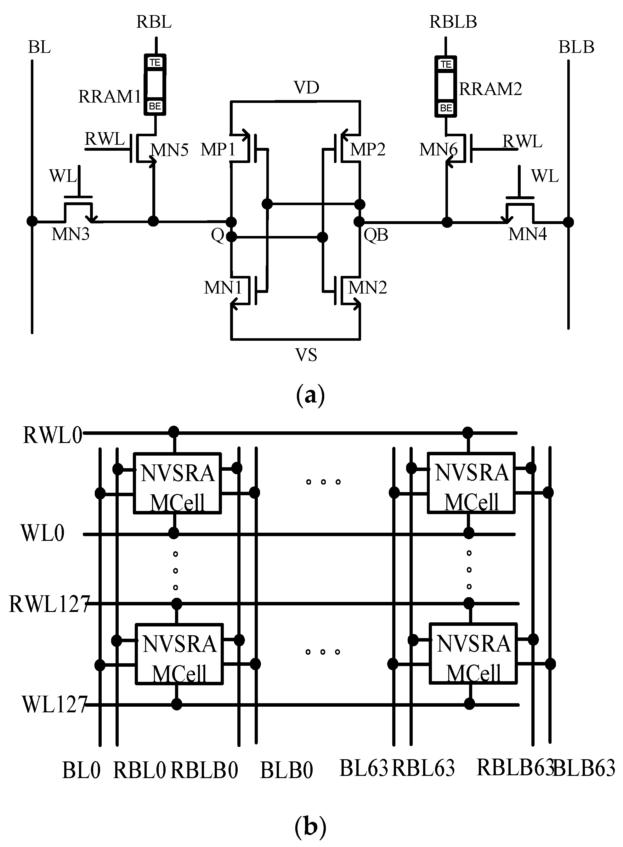
The memory cell of nvSRAM is mainly composed of SRAM and nonvolatile cells. The improved 8T2R nvSRAM memory cell proposed in this paper is shown in Figure 2. A pair of 1T1R RRAM are added to the traditional 6T SRAM storage nodes. While maintaining the traditional functions of SRAM, the data storage and data restoration functions are realized by controlling the memory cells of the RRAM. Different from the previous research, in the 1T1R structure, one end of the NMOS transistor is connected to the storage node, and the other end is connected to the lower electrode of the RRAM [22,23,24,25,26]. The gate of the transistor is controlled by the new signal RWL, and the upper electrode of two RRAMs is controlled by RBL and RBLB, respectively. Since bipolar RRAM is used, when the RRAM performs set and reset operations, different voltages are applied to the upper and lower electrodes of the RRAM to control the change in resistance. The upper electrode of the RRAM is introduced into independent control signals, and the resistance value of the RRAM is controlled through a driving circuit and power control circuit. Only when the RWL signal is turned on can the data of the SRAM and RRAM be transmitted, so that the static power consumption is zero when the NVM is not working. Under normal circumstances, nvSRAM performs read and write operations. Only when the voltage of the SRAM drops to a certain value, will the system switch to the data storage mode, and the data are stored in RRAM. The voltage required during this period is provided by the outside system. When the voltage of the SRAM is restored, the data restoration operation starts to restore the data in RRAM to the storage node of the SRAM. The Memory cell truth table is shown in Table 1.
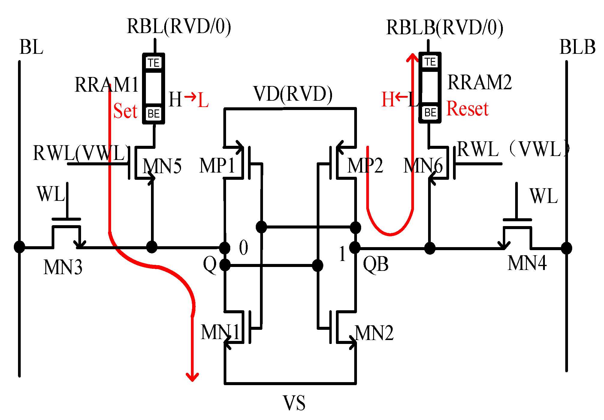
The principle of data storage operation is shown in Figure 3. When Q = 0, QB = 1, the supply voltage of nvSRAM is VD, WL and RWL are low, and nvSRAM maintains the data retention mode of SRAM at this time. Through turning off MN3 and MN4, the two bit lines free the data of the storage node from the interference of the BL and BLB signals. Meanwhile, RRAM1 and RRAM2 on both sides are in the state of high resistance and low resistance, respectively. When the system power supply fails, the nvSRAM enters the data storage mode. At this time, the voltage VD is switched to RVD, which is controlled by an independent power control circuit and is greater than VD. When the power supply rises, the voltage of storage node QB will rise to RVD with the change in power supply, while the voltage of Q is still 0. Both RBL and RBLB are connected to the read–write drive circuit of the RRAM. When the signal Store is valid and the signal Program is high, the voltage of RBL and RBLB becomes RVD through the control of the write drive circuit. When decoded by the address decoding control circuit, the RWL is high, making MN5 and MN6 turn on. Then, the upper electrode of RRAM1 is RVD, and its lower electrode is connected to storage node Q through the drain of MN5. While the voltage of storage node Q is 0, RRAM1 performs a set operation. This changes the resistance value of RRAM1 from high to low and completes the operation of writing 0. The upper electrode of RRAM 2 is also RVD, and its lower electrode is connected to storage node QB through the drain of MN6. Therefore, the voltage of storage node QB is RVD, which makes the voltage difference between the upper and lower electrodes of RRAM2 small, so RRAM2 maintains the current resistance value. Similarly, when signal Store is valid and signal Program is low, the voltage of RBL and RBLB becomes low through the control of the write drive circuit. After decoding by the address decoding control circuit, the RWL is high, which makes MN5 and MN6 on. At this time, the upper electrode of RRAM2 is low, and the lower electrode is connected to storage node QB through the drain of MN6. The voltage of storage node QB rises to RVD with the rise in the power supply voltage. The voltage difference between the lower and upper electrodes of RRAM2 is much greater than the reset voltage, so RRAM2 performs the reset operation. The resistance value of RRAM2 changes from low to high to complete the operation of writing 1. The upper electrode of RRAM1 is also 0, while the lower electrode is connected to storage node Q through the drain of MN5. The voltage of storage node Q is low, so that the voltage difference between the upper and lower electrodes of RRAM1 is small, and RRAM1 maintains the current resistance value.
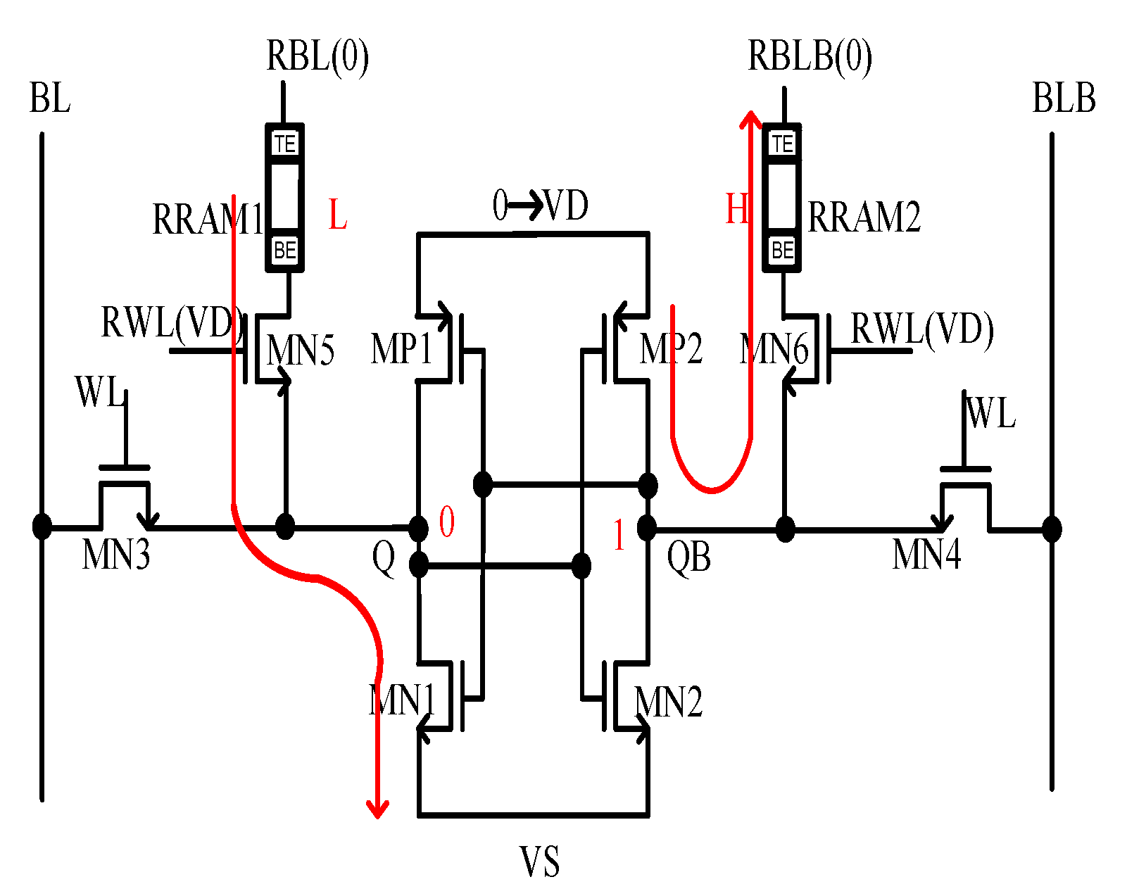
The principle of data restoration operation is shown in Figure 4. RRAM1 and RRAM2 are in the state of low resistance (L) and high resistance (H), respectively. Due to the failure of the nvSRAM system power supply, there are no data maintained in the storage node. When the power supply gradually rises from 0 to VD and the signal Restore is high, the voltage of RBL and RBLB becomes low through the control of the read drive circuit. After decoding, the RWL is high, which makes MN5 and MN6 turn on. RRAM1 and RRAM2 are in the state of low and high resistance, respectively. MN6 turns on and makes the voltage of RRAM2 gradually rise, while turning on MN5 makes the voltage of RRAM1 gradually lower. When the power supply of the nvSRAM system is restored, the voltage of the two storage nodes is restored to low and high, respectively.
When RRAM is forming, it is difficult to form all the memory cells in the same BL. This is due to the excessive load on the BL and the leakage of the device. Memory cells in a BL are divided into multiple modules to reduce the impact of the load. At the same time, memory cells are reset after forming back to HR status to reduce the leakage of the device and improve the success rate of cell forming.

3. nvSRAM Peripheral Circuit Design

3.1. Decoding Circuit

In this paper, a pre-decoding design is proposed to process the address signal by stages [27]. The first stage performs preprocessing, and then the second stage drives the output signal. Since the capacity of the memory is 8kb, there are 10 address decoding signals DIN0–DIN7, and eight input and output signals, I/O DIN0–DIN7 and DOUT0–DOUT7, respectively. Considering the need to share the SRAM address signal for decoding control of RRAM and the read–write driving ability of RRAM, the memory array is divided into 128 rows and 64 columns. The control of 128 row address signals requires 7-bit address signals (AIN0–AIN6). The column decoding circuit is jointly controlled by the address signal and I/O signal. AIN7–AIN9 can output eight groups of control signals through decoding of 3–8 decoder. Each group of signals controls an 8-bit row at the same time, and then controls different column signals through eight input or output signals, so as to complete the decoding operation of address rows and columns.
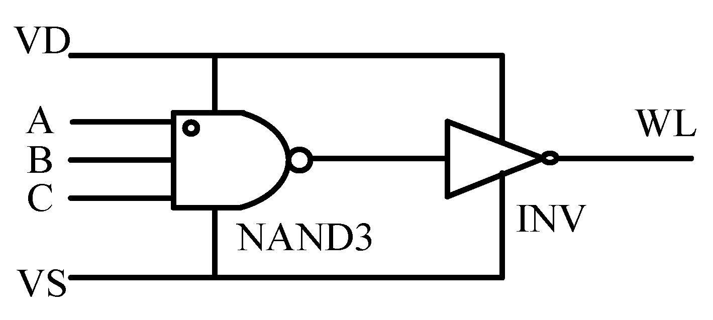
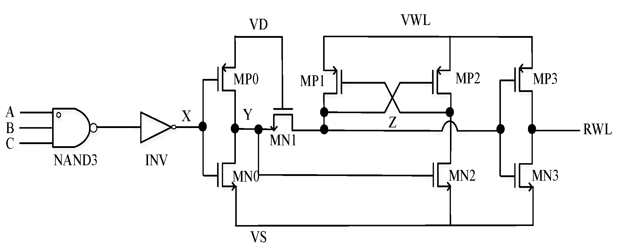
The row decoding circuit is shown in Figure 5, which consists of a three-input NAND and inverter. The NAND and inverter form the second-stage decoding circuit, which drives WL through a large inverter to improve the driving ability of WL. Because each row of the memory array shares the WL signal, it needs a row decoding circuit with large driving capacity to drive a whole row of WL signals. When the input signals A, B and C are high, and the NAND outputs low, the subsequent inverter outputs high to drive WL. When the input signal changes from A to XA <0:7>, and the input signal is high in turn while B and C are also high, WL <0:7> will be output in turn. Therefore, when XA <0:7>, XB <0:3> and XC <0:3> decode together, 128 WL decoding signals <0:127> can be generated.
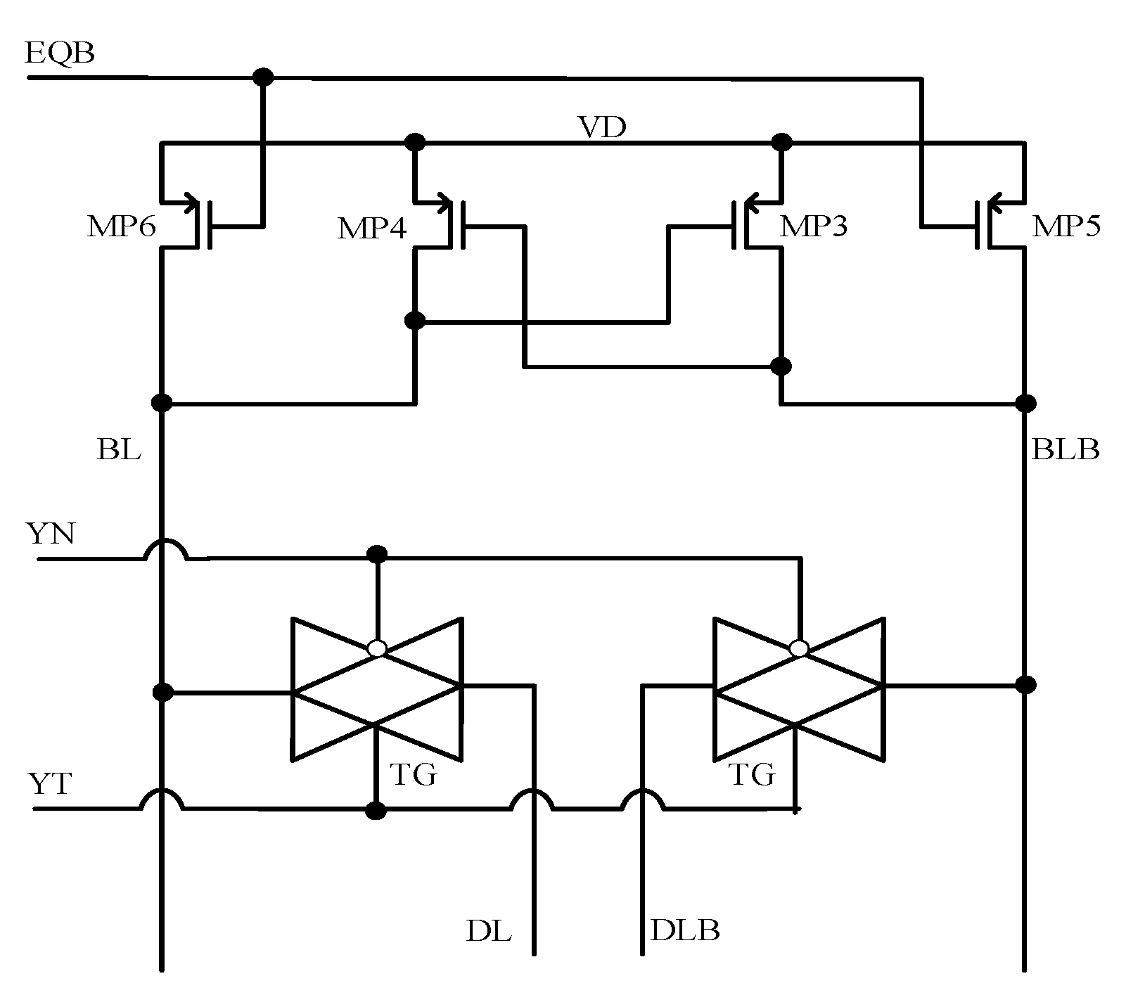
As shown in Figure 6, the column decoding circuit is mainly composed of two transmission gates and two PMOS for pre-charge [28]. The two transmission gates are controlled by the same set of YT and YN. The input of the transmission gate is BL and BLB, and the output is DL and DLB. DL and DLB are connected to the read–write control circuit. EQB is the gate control signal of MP6 and MP5, which controls the pre-charge switch of BL and BLB. When YT is low and YN is high, both transmission gates are on. While EQB is low, BL and BLB are charged to high. When EQB is high, the pre-charge process ends. Because there are 128 memory cells on the same BL, the pre-charge PMOS needs a larger size to ensure that the BL and BLB can be pulled up to high under large load. When the system reads and writes, it can control different column units by selecting different groups of YN and YT. YN and YT are generated by address and clock control signals.

3.2. Read Drive Circuit

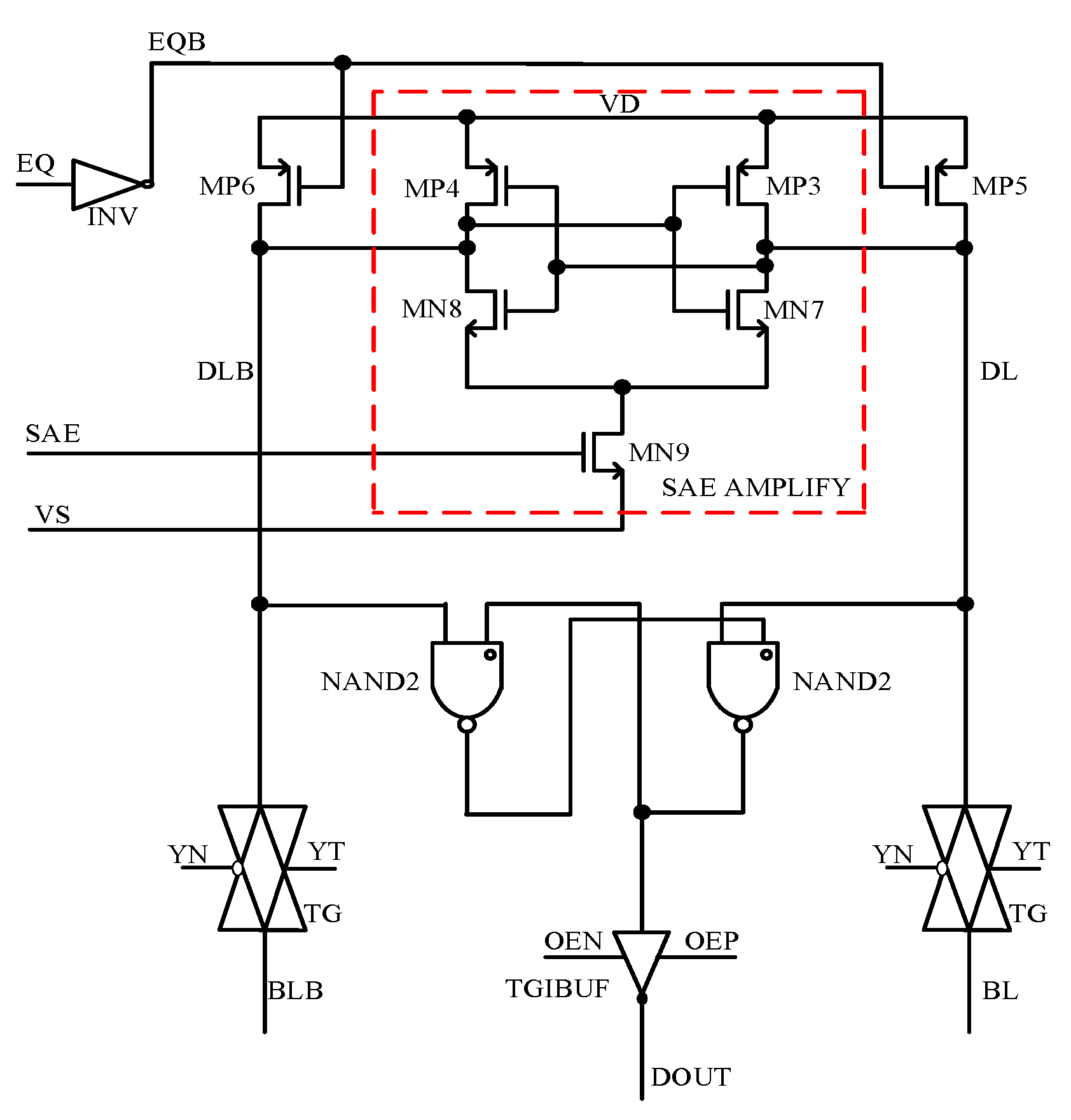
As shown in Figure 7, the read drive circuit includes a sensitive amplifier, latch and three-state gate [29]. The sensitive amplifier adopts a latch structure, which has faster speed compared with the traditional one. The voltage difference of the two bit lines is amplified by the sensitive amplifier, and the data are output through the latch and the three-state gate. SAE is the control signal. When SAE is high, the tail current source transistor turns on, and the sensitive amplifier starts to work. In read operation stage, when Q = 0 and QB = 1, EQB is low, and DL and DLB are pre-charged to high, DL and DLB output to BL and BLB by the three-state gate. When WL is on, because BL is high and storage node Q is low, BL forms a discharge path with the access and pull-down transistor, which will cause BL to produce a voltage drop. The voltage of BLB and QB remains the same. After rapid amplification by the sensitive amplifier, BL is low and BLB is high. When the BL and BLB voltages are transmitted to the input of the latch, the three-state gate outputs low, which completes the operation of reading 0. Similarly, when Q = 1 and QB = 0, after discharge of the memory cell, DL is high and DLB is low. After the two signals pass through the input of the latch, the latch outputs low, and the three-state gate outputs high, which completes the operation of reading 1. At the same time, when the latch input is high, the output maintains the data of the previous clock cycle until the next reading cycle. The latch of the next stage ensures the reliability of data read out by the memory cell in each clock cycle.

3.3. Write Drive Circuit

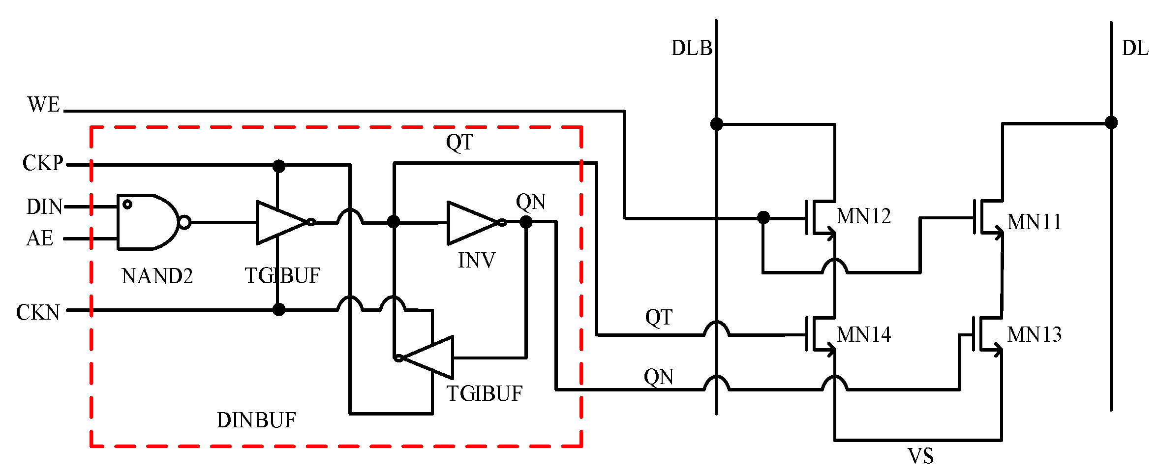
The write drive circuit is shown in Figure 8. The input buffer generates two reverse signals QN and QT through two input NANDs, a three-state gate and inverter. The outputs of QN and QT are controlled by the three-state gate. When the input DIN and AE are high, output is low. Meanwhile, the control signal CKP is low and CKN is high, so the three-state gate is on. Then, QT is high, and QN is low.
Before the write operation starts, DL and DLB are pulled to high through the pre-charge transistor. When the signal WE is high, the system enters the write operation mode. Then, MN12 and MN11 are on, and QT and QN are high and low, respectively. Therefore, a path is formed between DLB, MN12, MN14 and VS. DLB will be pulled down and output to BLB through the transmission gate. MN13’s off keeps BL high. When WL is on, BLB forms a discharge path, which flips the voltage of the memory cell QB. At the same time, the storage node Q will also reverse with the flip of QB, so that the node data of the memory cell change from Q = 0, QB = 1 to Q = 1, QB = 0, and the operation of writing 1 is completed. When QT is low and QN is high, DL forms a path to ground so that DL is low. DL and DLB are sent to BL and BLB through the transmission gate. At this time, BL is low, and BLB is high. The memory cell changes from Q = 1 and QB = 0 to Q = 0 and QB = 1 after internal discharge, and the operation of writing 0 is completed.

3.4. Data Storage and Restoration Circuit

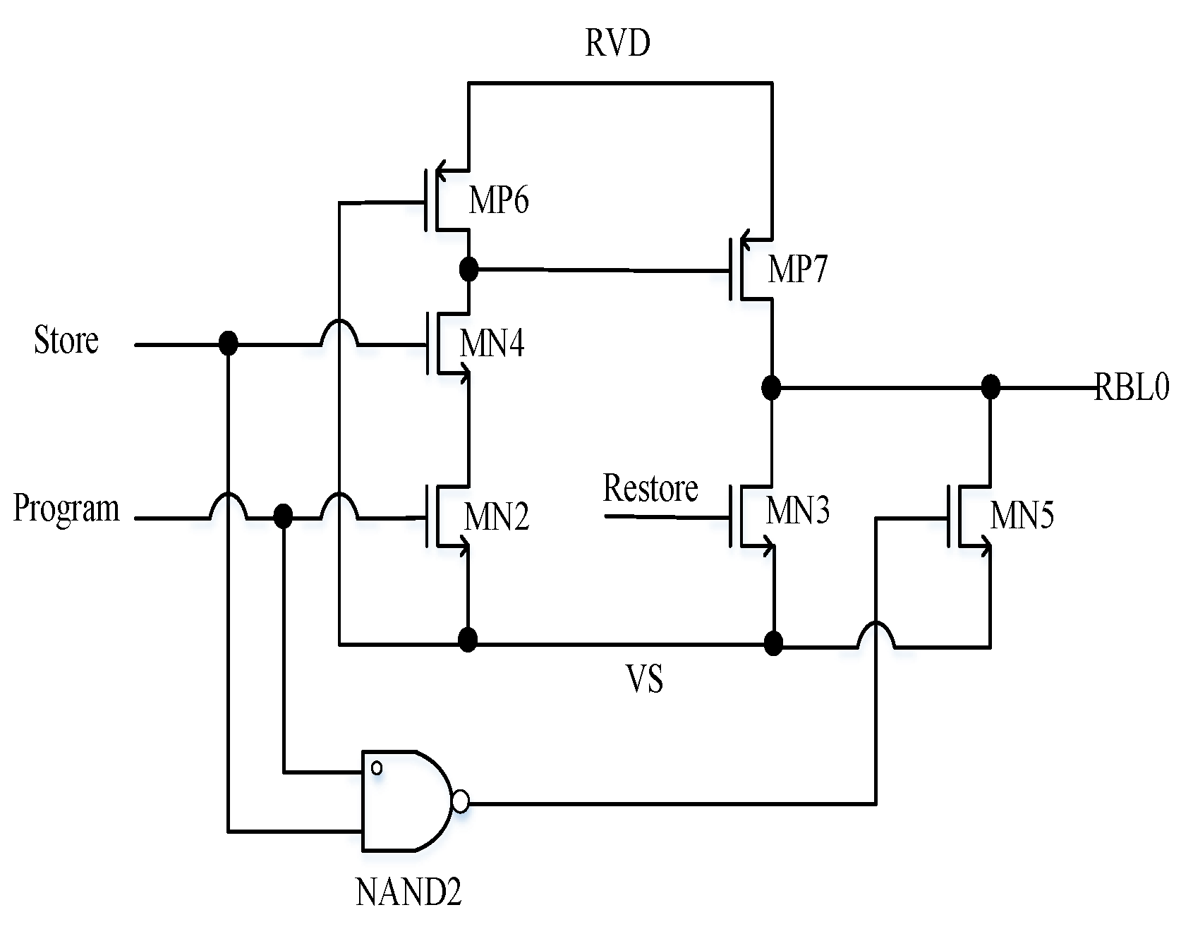
The data storage and restoration circuit mainly includes a RRAM read/write drive circuit and decoding drive circuit, as shown in Figure 9. RVD is the system input, and MP6 and MP7 are MOS transistors of 2.5 V. The output of RBL0 is driven by controlling input signals such as Store, Program, and Restore. When Store, Program and Restore are low, MN5 turns on, and RBL0 is low, so the system maintains the normal operation mode of SRAM. When Store/Program is high and Restore is low, MP7 is on, and MN3 and MN5 are off. Then, RBL0 is pulled up to RVD due to MP7. While RWL is valid, RRAM is in set operation mode. Since Program becomes low, MN5 is turned on, and RBL0 is pulled down to low, which make RRAM enter reset operation mode. In case Store/Program is low and Restore is high, MN3 and MN5 are on, RBL0 is pulled down, and the system is in data restoration mode when RWL is valid.
RRAM will share the address signal with SRAM during decoding. When RRAM performs set and reset operations, the voltage of RWL will be greater than the system power supply VD of nvSRAM, so RWL needs an independent voltage driving circuit. The driving circuit of RWL is shown in Figure 10 [30]. MN0 and MP0 are 0.9 V MOS transistors. MN1, MN2, MN3, MP1, MP2 and MP3 are 2.5 V MOS transistors. Additionally MN1 is a MOS transistor with low threshold voltage, which isolates the voltage of Y and Z nodes to prevent device damage. While the input signals A, B and C are all VD, the voltage at X is VD. Then, the voltage at Y and Z is 0 through the inverter. Since MP3 is turned on, RWL is pulled up to VWL, and RRAM is driven to set or reset operation.

4. Experimental Results

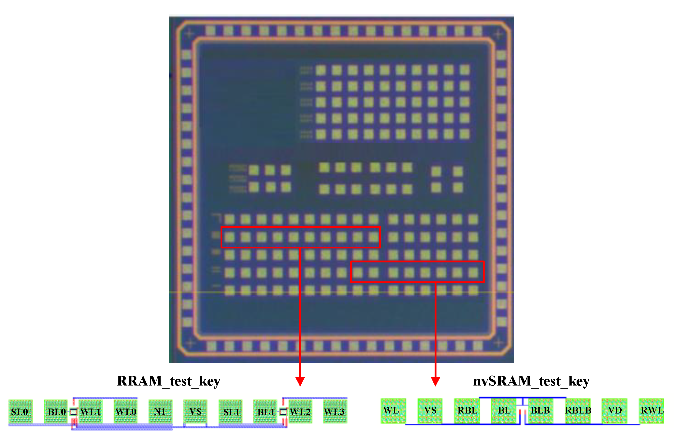
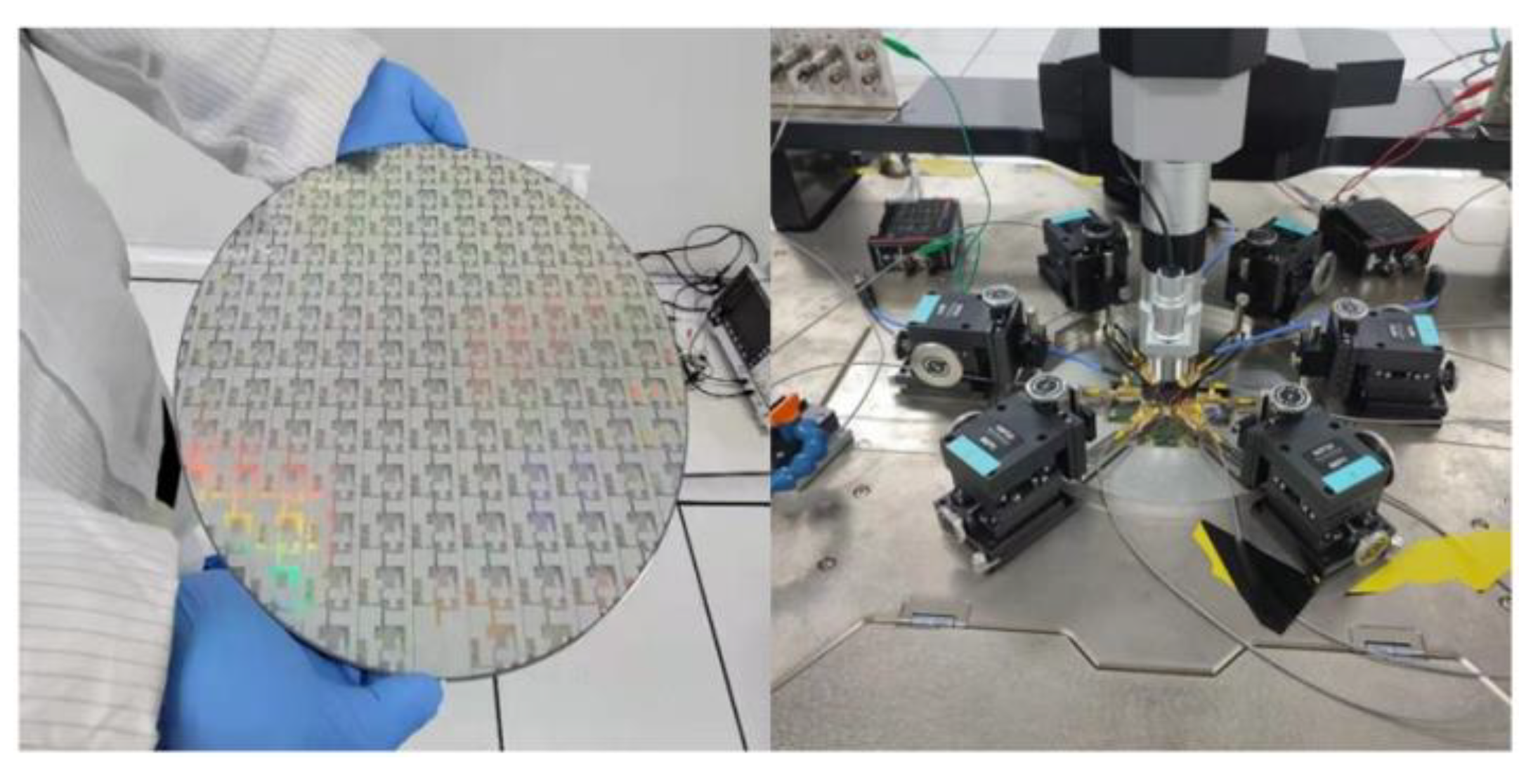
The memory cell and array are the core of the whole nvSRAM. Additionally, the control voltage of the memory cell must first be determined, so as to design the peripheral circuit. The proposed nvSRAM was fabricated using a 28 nm 1P9M CMOS process. The material of the RRAM was Ti/Al2O3/HfO2, and its size was 110 nm × 110 nm with a three-layer structure. The test was performed separately for 1T1R RRAM and nvSRAM [31]. Figure 11 shows a micrograph of all test chips. The nvSRAM die and test environment are shown in Figure 12. Figure 13, Figure 14 and Figure 15 shows the test results for RRAM, and Figure 16, Figure 17 and Figure 18 are simulation results.
In order to determine the peripheral operating conditions of the memory cell, firstly the RRAM was tested and analyzed. Before the RRAM performed set and reset operations, the device had to be formed to make the resistive material conductive. During the set operation, the current had to be limited to RRAM to prevent the over-forming phenomenon, which may have resulted in reset failure. The following test was the test after each RRAM was successfully formed. The DC test was carried out for RRAMs in different areas, and multiple cycle test analysis was performed at the same time to reduce the randomness of data caused by process errors.
Figure 13a is a 20-cycle test of RRAM. The test data show that when the voltage was less than 0.7 V, RRAM completed the change from high resistance to low resistance. When the voltage was less than 0.9 V, RRAM completed the change from low resistance to high resistance. Compared with the test data for the first 10 cycles, it was found that the resistance window for the last 10 cycles of RRAM was obviously better. Figure 13b,c are the tests of 10 cycles of RRAM, respectively, and the current limit of set was adjusted to 150 μA and 200 μA, respectively.
The test results from the first and last five cycles show that the resistance window of the last five cycles was indeed larger than that of the first few cycles, which means that more cycle tests could make the memory cell have a larger resistance window and stronger data stability.
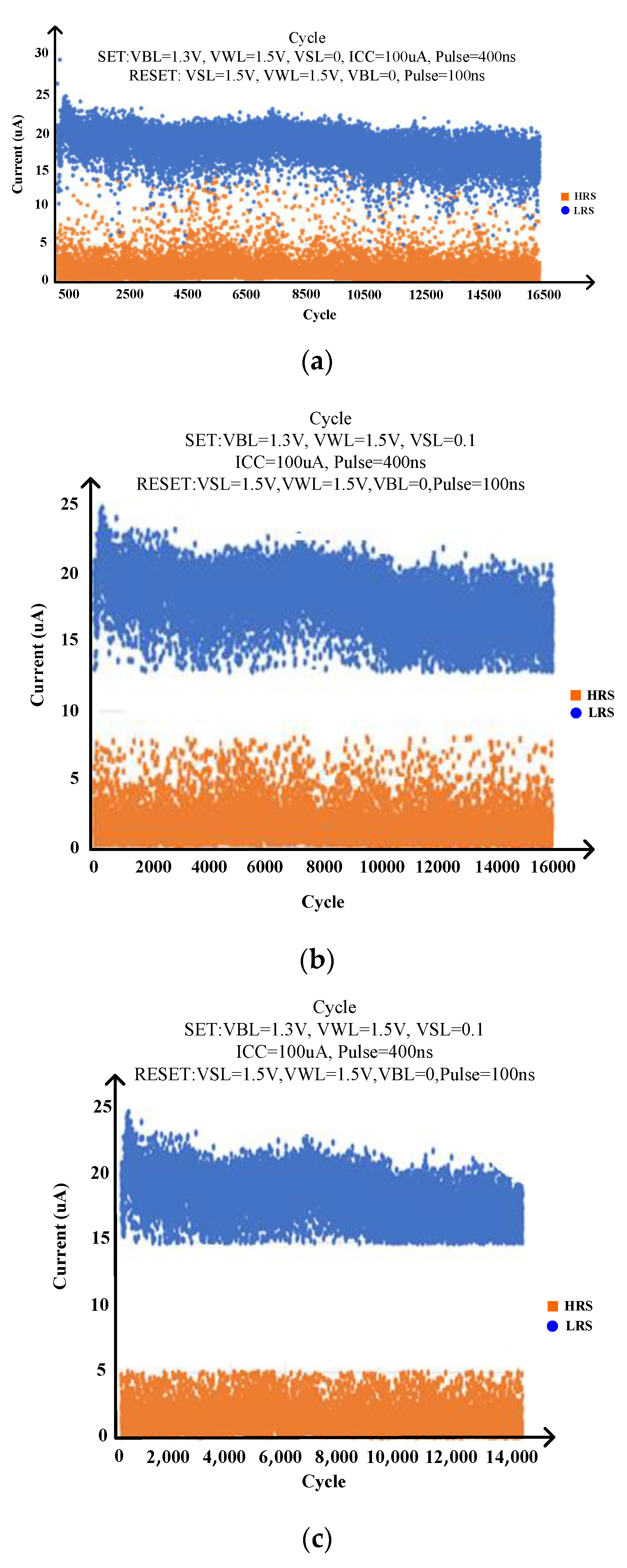
To more accurately test the conditions of the set and reset operations of RRAM with 1T1R structure, a pulse mode is used. Then, RRAM in different dies was tested with the cycle test, and the current distribution of high/low resistance was counted. Figure 14a is the original data of cycle test. The current of the RRAM was about 15 μA when the resistance was low and about 5 μA when the resistance was high. At the same time, there were few resistance differences. Figure 14b shows the current distribution after removing the data with high-resistance current greater than 8 μA and low-resistance current lower than 15 μA, respectively. Figure 14c shows the current distribution after removing the data with high-resistance current greater than 5 μA and low-resistance current lower than 13 μA, respectively.
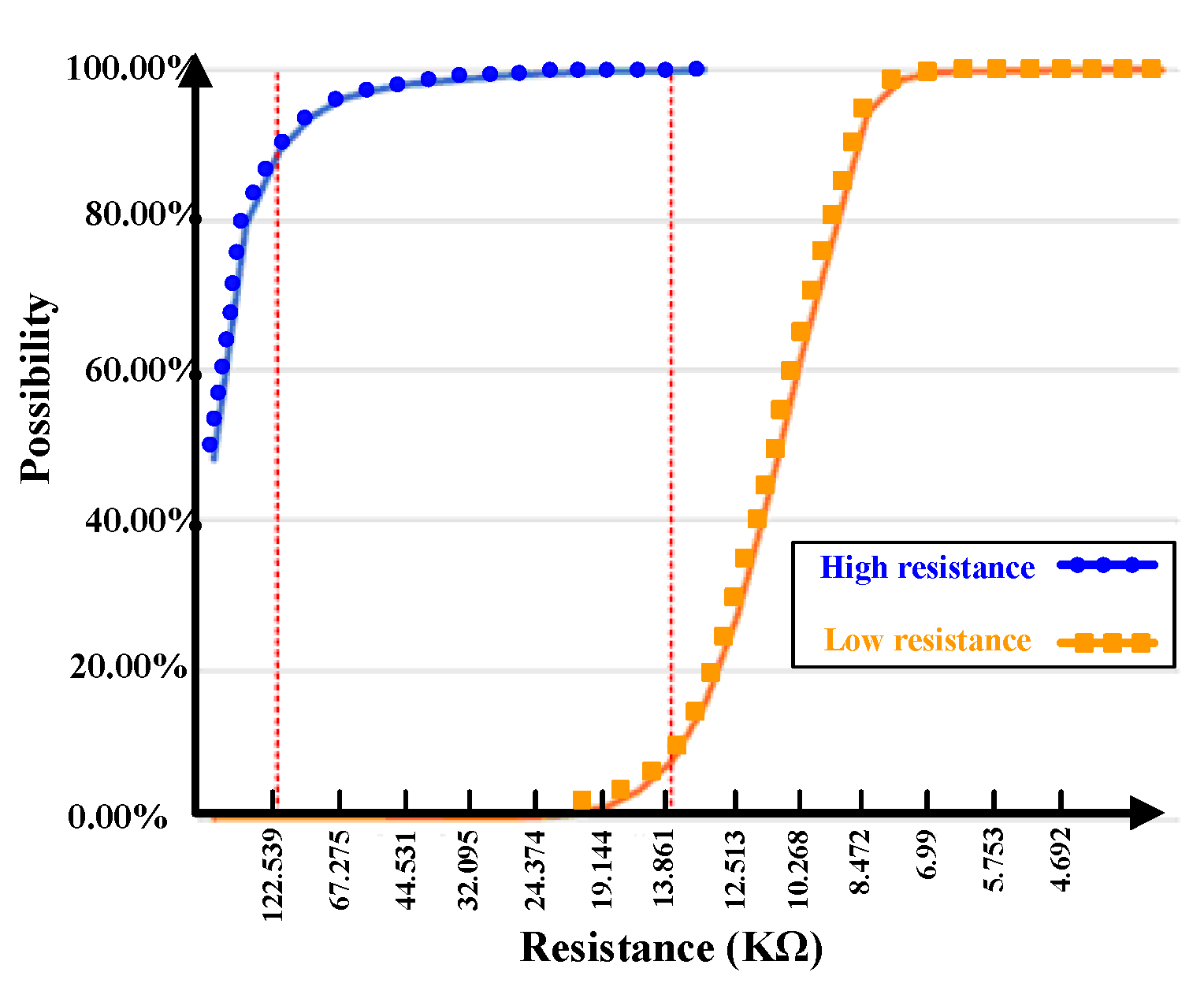
The current distribution diagram was transformed into the corresponding resistance value distribution, as shown in Figure 15. It can be seen from the distribution of resistance values that 90% of the resistance values of high resistance and low resistance were about 10 times the resistance of the window, and the data had good stability.
At room temperature, the resistance values of 1024 bit HR and LR were counted, respectively, as shown in Figure 16. The average value of HR was 94.7 K, and the average value of LR was 12.7 K. The resistance windows of HR and LR indicated that the RRAM had good storage characteristics.
From the DC test results for the RRAM, it was determined that when a separate RRAM performed a set operation, a voltage of about 0.7 V was required to complete the set operation, and the voltage for the reset was 0.9 V. According to the test results for the 1T1R RRAM, when VWL = 1.5 V, the set voltage was 1.3 V, the current limit was 100 μA, and the reset voltage was 1.5 V. Based on above data analysis, and considering the influence of signal loss, the basic principle of circuit design in this paper was that the Vset and Vreset voltages of the RRAM were 1.6 V, and the voltage of VWL was controlled by a separate RWL driving circuit.
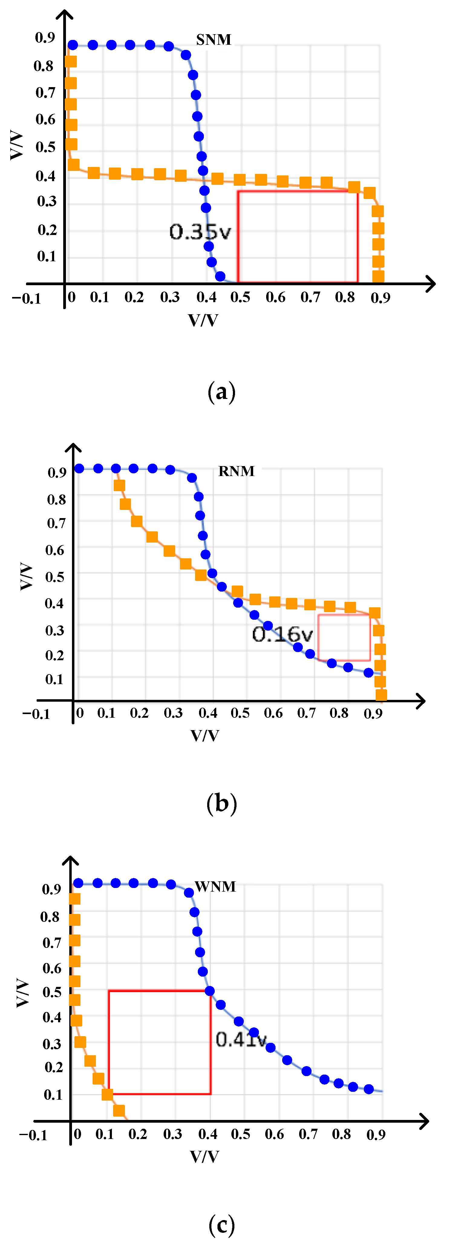
Based on the VTC test method, the noise margin of the memory cell was as shown in Figure 17. When the power supply voltage was 0.9 V, the static noise margin (SNM) was 0.35 V, read noise margin (RNM) 0.16 V, and write noise margin (WNM) 0.41 V. After adding the 1T1R RRAM, the memory cell still had good data anti-interference ability.
The simulation results for the data storage and restoration circuit are shown in Figure 18. First, a data 0 is written into the selected memory cell through the write mode of the SRAM. When the system fails, nvSRAM enters the data storage mode. By controlling the power module and the RBL driver module, the RRAM performs set and reset operations, respectively, to write the data of the storage node to RRAM. When the system enters pre-charge mode, the data of the SRAM storage node are lost. When the restore mode is entered, the data are restored to the storage node of SRAM through the control circuit module and RBL drive module.
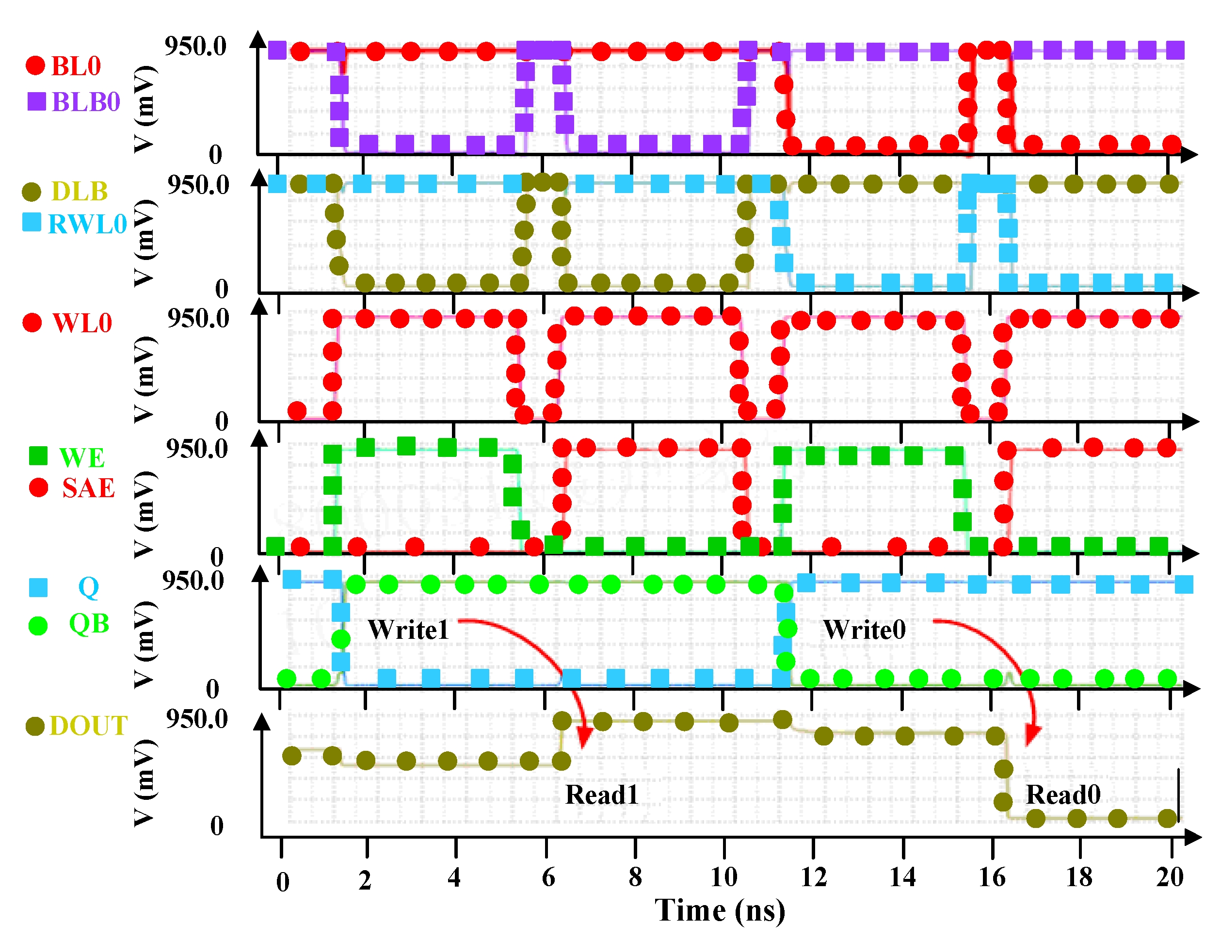
The simulation results for the nvSRAM read–write circuit are shown in Figure 19. Firstly, the memory cell is selected through the decoding circuit, then the data are written into it through I/O and the write driving circuit. After that, the data are read out by controlling the read driving circuit. While writing the data to the memory cell in one cycle, in the next cycle, the system reads the data. The time from writing to reading is 5.2 ns. In the figure, WE is the write control signal, SAE is the switch signal of the sensitive amplifier, and DOUT is the output.
A performance comparison between the improved 8T2R nvSRAM proposed in this paper and the previous nvSRAM is shown in Table 2. The memory cell has low power supply voltage, low power consumption and high density. As with other traditional processes, its characteristic size is basically the same. Compared with the nvSRAM of other structures, our memory cell has faster data storage and restoration times that make the data storage and restoration operations more efficient and reduce the risk of data loss.

5. Conclusions

This paper presented an improved 8T2R nvSRAM memory cell structure based on RRAM technology for the application of new memory. Aiming at the problem where the data in the SRAM cannot be restored after a power failure, RRAM technology is introduced into the SRAM. The data in the SRAM are stored in RRAM before power failure. When the power supply is restored, the data are restored to SRAM, which solves the disadvantage of SRAM volatility. Meanwhile, a proposed pre-decoding technique improves the reading and writing speed. The memory cell was realized with a UMC CMOS 28 nm 1P9M process, occupying only 0.97 μm2. The simulation results show that when the power supply voltage is 0.9 V, the static noise margin is 0.35 V, the read noise margin is 0.16 V, and the write noise margin is 0.41 V. Additionally, the data storage time is 0.21 ns and restoration time is 0.18 ns. Further, a peripheral circuit was designed, and an 8kb nvSRAM realized. The time for the system to read 1 bit data is 5.2 ns. Compared with the previous research results, it has lower power consumption and faster data storage and restoration times, thus increasing the stability of data storage. This work only verified the design of the memory cell and peripheral circuit from the aspect of function, which had certain limitations. The nvSRAM array was only simulated. Since a differential structure requires a forming process before reading and writing, and the voltage of forming is high, we should also consider the impact of the forming process, so that the design will be more conducive to the read speed of the SRAM. In the design of nvSRAMs based on RRAM technology, most designs use the high and low resistance states of RRAM to store data. This single mode makes the SRAM and RRAM combination a one-to-many mode. However, research found that RRAM has a multi-value storage feature, that is, a single RRAM can store multi-bit data. This discovery provides a new idea for the design of nvSRAM, that is, multiple SRAM cells can share one or two RRAMs to realize the non-volatile storage function.

Author Contributions

Conceptualization, C.C.; funding acquisition, C.C. and J.J.; methodology, J.Y., W.L. and Y.Z.; project administration, J.Y., W.L. and Y.Z.; resources, Y.Z.; software, C.C. and J.J.; supervision, C.C. and J.J.; validation, C.C. and J.J.; writing—original draft, J.Y.; writing—review and editing, C.C. and J.J. All authors have read and agreed to the published version of the manuscript.

Funding

This research was funded by Jihua laboratory Fund Project (2021B0301030003-03), Xiamen Youth Innovation Fund Project (3502Z20206074) and Major science and technology projects of Xiamen (3502Z20221022).

Institutional Review Board Statement

Not applicable.

Informed Consent Statement

Not applicable.

Data Availability Statement

Not applicable.

Conflicts of Interest

The authors declare no conflict of interest.

References

  1. Wong, G. Flash Memory Trends; Flash Memory Summit: Santa Clara, CA, USA, 2008. [Google Scholar]
  2. Meena, J.S.; Sze, S.M.; Chand, U.; Tseng, T.-Y. Overview of emerging nonvolatile memory technologies. Nanoscale Res. Lett. 2014, 9, 526–559. [Google Scholar] [CrossRef] [Green Version]
  3. Garbin, D.; Vianello, E.; Bichler, O.; Rafhay, Q.; Gamrat, C.; Ghibaudo, G.; DeSalvo, B.; Perniola, L. HfO2-Based OxRAM Devices as Synapses for Convolutional Neural Networks. IEEE Trans. Electron Devices 2015, 62, 2494–2501. [Google Scholar] [CrossRef]
  4. Bocquet, M.; Deleruyelle, D.; Aziza, H.; Muller, C.; Portal, J.-M.; Cabout, T.; Jalaguier, E. Robust Compact Model for Bipolar Oxide-Based Resistive Switching Memories. IEEE Trans. Electron Devices 2014, 61, 674–681. [Google Scholar] [CrossRef]
  5. Fliesler, M.; Still, D.; Hwang, J. A 15ns 4Mb nvSRAM in 0.13u SONOS Technology; Non-Volatile Semiconductor Memory Workshop: Opio, France, 2008; pp. 83–86. [Google Scholar]
  6. Sakimura, N.; Sugibayashi, T.; Nebashi, R.; Kasai, N. Nonvolatile magnetic flip-flop for standby-power free SoCs. IEEE J. Solid-State Circuits 2009, 44, 2244–2250. [Google Scholar] [CrossRef]
  7. Miwa, T.; Yamada, J.; Koike, H.; Toyoshima, H.; Amanuma, K.; Kobayashi, S.; Tatsumi, T.; Maejima, Y.; Hada, H.; Kunio, T. NV-SRAM: A nonvolatile SRAM with backup ferroelectric capacitors. IEEE J. Solid-State Circuits 2001, 36, 522–527. [Google Scholar] [CrossRef]
  8. Choi, B.J.; Torrezan, A.C.; Strachan, J.P.; Kotula, P.G.; Lohn, A.J.; Marinella, M.J.; Li, Z.; Williams, R.S.; Yang, J.J. High-speed and low-energy nitride memristors. Adv. Funct. Mater. 2016, 26, 5290–5296. [Google Scholar] [CrossRef] [Green Version]
  9. Pi, S.; Li, C.; Jiang, H.; Xia, W.; Xin, H.; Yang, J.J.; Xia, Q. Memristor crossbar arrays with 6-nm half-pitch and 2-nm critical dimension. Nat. Nanotechnol. 2019, 14, 35–39. [Google Scholar] [CrossRef]
  10. Govoreanu, B.; Kar, G.S.; Chen, Y.-Y.; Paraschiv, V.; Kubicek, S.; Fantini, A.; Radu, I.P.; Goux, L.; Clima, S.; Degraeve, R. 10 × 10 nm2 Hf/HfOx crossbar resistive RAM with excellent performance, reliability and low-energy operation. In Proceedings of the 2011 International Electron Devices Meeting, Washington, DC, USA, 5–7 December 2011. [Google Scholar]
  11. Prezioso, M.; Merrikh-Bayat, F.; Hoskins, B.D.; Adam, G.C.; Likharev, K.K.; Strukov, D.B. Training and operation of an integrated neuromorphic network based on metal-oxide memristors. Nature 2015, 521, 61–64. [Google Scholar] [CrossRef] [Green Version]
  12. Covi, E.; Brivio, S.; Serb, A.; Prodromakis, T.; Fanciulli, M.; Spiga, S. Analog memristive synapse in spiking networks implementing unsupervised learning. Front. Neurosci. 2016, 10, 482. [Google Scholar] [CrossRef] [Green Version]
  13. Yang, Y.; White, M.H. Charge retention of scaled SONOS nonvolatile memory devices at elevated temperatures. Solid State Electron. 2000, 44, 949–958. [Google Scholar] [CrossRef]
  14. Shimomura, N.; Yoda, H.; Ikegawa, S.; Kai, T.; Amano, M.; Aikawa, H.; Ueda, T.; Nakayama, M.; Asao, Y.; Hosotani, K.; et al. Switching current fluctuation and repeatabitity for MRAM with propeller-shape MTJ. IEEE Trans. Magn. 2006, 42, 2757–2759. [Google Scholar] [CrossRef]
  15. Waser, R.; Aono, M. Nanoionics-based resistive switch memories. Nat. Mater. 2007, 6, 833–840. [Google Scholar] [CrossRef]
  16. Bazzi, H.; Harb, A.; Aziza, H.; Moreau, M.; Kassem, A. RRAM-based non-volatile SRAM cell architectures for ultra-low-power applications. Analog. Integr. Circuits Signal Process. 2020, 106, 351–361. [Google Scholar] [CrossRef]
  17. Chang, M.-F.; Lee, A.; Kuo, C.-C.; Sheu, S.-S.; Chen, F.T.; Ku, T.-K.; Liu, Y.-P.; Yang, H.-Z.; Chen, P.-C. Challenges at circuit designs for resistive-type Nonvolatile memory and nonvolatile logics in mobile and cloud applications. In Proceedings of the 2014 12th IEEE International Conference on Solid-State and Integrated Circuit Technology (ICSICT), Guilin, China, 28–31 October 2014; pp. 1–4. [Google Scholar]
  18. Chen, W.-H.; Khwa, W.-S.; Li, J.-Y.; Lin, W.-Y.; Lin, H.-T.; Liu, Y.; Wang, Y.; Wu, H.; Yang, H.; Chang, M.-F. Circuit design for beyond von Neumann applications using emerging memory: From nonvolatile logics to neuromorphic computing. In Proceedings of the 2017 18th International Symposium on Quality Electronic Design (ISQED), Santa Clara, CA, USA, 14–15 March 2017; pp. 23–28. [Google Scholar]
  19. Wong, H.S.P. Metal-oxide RRAM. Proc. IEEE 2012, 100, 1951–1970. [Google Scholar] [CrossRef]
  20. Zhuang, W.W.; Pan, W.; Ulrich, B.D.; Lee, J.J.; Stecker, L.; Burmaster, A.; Evans, D.R.; Hsu, S.T.; Tajiri, M.; Shimaoka, A.; et al. Novel colossal mangetoresistive thin film nonvolatile resistance random access memory (RRAM). In Proceedings of the International Electron Devices Meeting, San Francisco, CA, USA, 8–11 December 2002; pp. 193–196. [Google Scholar]
  21. Burrb, G.W.; Shenoyc, R.S.; Virwani, K.; Narayanan, P.; Padillad, A.; Kurdi, B. Access devices for 3D cross point memory. J. Vac. Sci. Technol. B Nanotechnol. Microelectron. Mater. Process. Meas. Phenom. 2014, 32, 040802. [Google Scholar] [CrossRef] [Green Version]
  22. Wei, W.; Namba, K.; Han, J.; Lombardi, F. Design of a Nonvolatile 7T1R SRAM Cell for Instant-on Operation. IEEE Trans. Nanotechnol. 2014, 13, 905–916. [Google Scholar] [CrossRef]
  23. Ielmini, D. Resistive switching memories based on metal oxides: Mechanisms, reliability and scaling. Semicond. Sci. Technol. 2016, 31, 3002. [Google Scholar] [CrossRef]
  24. Lee, A.; Chang, M.F.; Lin, C.C.; Chen, C.F.; Ku, T.K. RRAM-based 7T1R nonvolatile SRAM with 2x reduction in store energy and 94x reduction in restore energy for frequent-off instant-on applications. In Proceedings of the 2015 Symposium on VLSI Circuits (VLSI Circuits), Kyoto, Japan, 17–19 June 2015; pp. 76–77. [Google Scholar]
  25. Tosson, A. 8T1R: A novel low -power High-speed RRAM based non-volatile SRAM design. In Proceedings of the IEEE International International Great Lakes Symposium on VLSI (GLSVLSI), Houston, TX, USA, 21–23 May 2016; pp. 239–244. [Google Scholar]
  26. Turkyilmaz, O.; Onkaraiah, S.; Reyboz, M. RRAM-based FPGA for “normally of, instantly on” applications. In Proceedings of the 2012 IEEE/ACM International Symposium on Nanoscale Architectures, Amsterdam, The Netherlands, 4–6 July 2012; pp. 101–108. [Google Scholar]
  27. Nambu, H.; Kanetani, K.; Yamasaki, K.; Higeta, K.; Usami, M.; Fujimura, Y.; Ando, K.; Kusunoki, T.; Yamaguchi, K.; Homma, N.; et al. A 1.8-ns Access, 550-MHz, 4.5-Mb CMOS SRAM. IEEE J. Solid State Circuits 1998, 33, 1650–1658. [Google Scholar] [CrossRef]
  28. Martin, K. Digital Integrated Circuit Design; Oxford University Press: New York, NY, USA, 2000. [Google Scholar]
  29. Wang, N.N. On the Design of MOS Dynamic Sens e Amplifiers. IEEE Trans. On Circuits and Systems 2000, 29, 467–477. [Google Scholar] [CrossRef]
  30. Ioth, K. VLSI Memory Design; Baifukan: Tokyo, Japan, 1994. [Google Scholar]
  31. Ravi, V.; Prabaharan, S.R.S. Memristor based memories: Defects, testing, and testability techniques. Far East J. Electron. Commun. 2017, 17, 105–125. [Google Scholar] [CrossRef]
  32. Sheu, S.S.; Kuo, C.C.; Chang, M.F.; Tseng, P.L.; Sheng, L.C.; Wang, M.C.; Lin, C.H.; Lin, W.P.; Chien, T.K.; Lee, S.H.; et al. A ReRAM integrated 7T2R non-volatile SRAM for normally-off computing application. In Proceedings of the 2013 IEEE Asian Solid-State Circuits Conference (A-SSCC), Singapore, 11–13 November 2013; pp. 245–248. [Google Scholar]
  33. Chiu, P.-F.; Chang, M.-F.; Wu, C.-W.; Chuang, C.-H.; Sheu, S.-S.; Chen, Y.-S.; Tsai, M.-J. Low Store Energy, Low VDDmin,8T2R Nonvolatile Latch and SRAM with Vertical-Stacked Resistive Memory (Memristor) Devices for Low Power Mobile Applications. J. Solid-State Circuits 2012, 47, 1483–1496. [Google Scholar] [CrossRef]
  34. Majumdar, S.; Kingra, S.K.; Suri, M.; Tikyani, M. Hybrid CMOS-OxRAM based 4T-2R NVSRAM with efficient programming scheme. In Proceedings of the 2016 16th Non-Volatile Memory Technology Symposium (NVMTS), Pittsburgh, PA, USA, 17–19 October 2016; pp. 1–4. [Google Scholar]
Figure 1. nvSRAM system structure.
Applsci 13 00531 g001
Figure 2. (a) 8T2R nvSRAM memory cell, (b) 128 × 64 array.
Applsci 13 00531 g002
Figure 3. Data storage operation.
Applsci 13 00531 g003
Figure 4. Data restoration operation.
Applsci 13 00531 g004
Figure 5. Row decoding circuit.
Applsci 13 00531 g005
Figure 6. Column decoding circuit.
Applsci 13 00531 g006
Figure 7. Read drive circuit.
Applsci 13 00531 g007
Figure 8. Write driver circuit.
Applsci 13 00531 g008
Figure 9. RRAM read/write drive circuit.
Applsci 13 00531 g009
Figure 10. RWL driving circuit.
Applsci 13 00531 g010
Figure 11. Micrograph of all test chip.
Applsci 13 00531 g011
Figure 12. Die of nvSRAM and test environment.
Applsci 13 00531 g012
Figure 13. DC test results for 1T1R RRAM: (a) 20 cycles (current:100 μA); (b) 10 cycles (current: 150 μA); (c) 10 cycles (current: 200 μA).
Applsci 13 00531 g013
Figure 14. Pulse test results for 1T1R RRAM: (a) original data; (b) the data after removing the data of high-resistance current greater than 8 μA and low-resistance current lower than 15 μA; (c) data with high-resistance current greater than 5 μA and low-resistance current lower than 13 μA after data removal.
Applsci 13 00531 g014
Figure 15. Resistance distribution diagram of RRAM.
Applsci 13 00531 g015
Figure 16. Distribution of HR and LR values.
Applsci 13 00531 g016
Figure 17. Noise margin: (a) static noise margin; (b) read noise margin; (c) write noise margin.
Applsci 13 00531 g017
Figure 18. Simulation results for data storage and restoration circuit.
Applsci 13 00531 g018
Figure 19. Simulation results for reading and writing speed.
Applsci 13 00531 g019
Table 1. Memory cell truth table.
ModeBLBLBWLRBLRBLBRWLVD
Hold0.90.900000.9
Read(1)0.900.90000.9
Read(0)00.90.90000.9
Write(1)0.900.90000.9
Write(0)00.90.90000.9
Store0.90.901.6/01.6/00.91.6
Restore0.90.90000.90.9
Table 2. Performance comparison of different nvSRAMs.
This work[16][32][33][22][34]
Memory cell structure8T2R6T2R7T2R8T2R7T1R4T2R
Technology 28 nm
UMC
130 nm
STM
0.18 μm TSMC0.18 μm
TSMC
32 nm90 nm
Power supply0.9 V1.8 V0.7 V1.8 V0.9 V4 V
Restoration modeDifferential DifferentialDifferentialDifferentialSingleDifferential
Nonvolatile modeBefore power failureReal timeBefore power failureBefore power failureBefore power failureReal time
Storage time0.21 ns 1 ns0.87 ns0.24 ns1.45 ns
Restoration time0.18 ns 0.37 ns0.36 ns0.22 ns0.02 ns
Current (when storing data)0–200 μA0–50 μA0–230 μA0–260 μA0–40 μA0–230 μA
Voltage (when storing data)1.6 V1.8 V2.5 V4.0 V2.0 V1.5 V
Memory cell size0.97 μm232.6 μm21 μm21.55 μm21.18 μm20.6 μm2
Disclaimer/Publisher’s Note: The statements, opinions and data contained in all publications are solely those of the individual author(s) and contributor(s) and not of MDPI and/or the editor(s). MDPI and/or the editor(s) disclaim responsibility for any injury to people or property resulting from any ideas, methods, instructions or products referred to in the content.