Article

Lightweight Omnidirectional Radiation Protection for a Photon-Counting Imaging System in Space Applications

1
Changchun Institute of Optics, Fine Mechanics and Physics, Chinese Academy of Sciences, Changchun 130033, China
2
University of Chinese Academy of Sciences, Beijing 100049, China
*
Authors to whom correspondence should be addressed.
Appl. Sci. 2023, 13(10), 5905; https://doi.org/10.3390/app13105905
Submission received: 23 February 2023 / Revised: 25 April 2023 / Accepted: 25 April 2023 / Published: 10 May 2023
(This article belongs to the Special Issue Advanced Optoelectronic Devices and Systems)

Abstract

:
Concerns about the impact of space radiation on spacecraft and their internal instruments have prompted the need for effective protection. However, excessive protection can increase the costs and difficulty of space launches, making it crucial to achieve better shielding protection of lighter weights. In real space orbits, we observed the interference of charged particles on photon-counting imaging detectors and plan to address this issue by adding a shielding ring to the side wall of the detector input terminal. Additionally, a local protection structure was proposed for electronics, where the outer edge was increased to enable particles to reach the same thickness as the shielding box within the PCB range. This approach resulted in an omnidirectional spatial shielding thickness that was nearly identical at any point on the PCB surface. Furthermore, we used the Monte Carlo method to calculate the energy loss of electrons and protons in materials such as aluminum (Al), tantalum (Ta), and high-density polyethylene (HDPE). Through this analysis, we determined the optimal mass ratio of Al, Ta, and HDPE to achieve the lowest ionization doses at an object’s location in the particle environment of the FY-3 satellite orbit. This protection strategy provides a useful design concept for photoelectric detection instruments with high sensitivity.

1. Introduction

A photoelectric device will be subjected to a variety of challenging space radiation environments, including exposure to the inner and outer Van Allen radiation belts surrounding the Earth, as well as solar and galactic cosmic rays, plasma radiation, ultraviolet radiation, and other forms of radiation [1,2]. The South Atlantic Anomaly (SAA), located at a longitude 90° W to 20° E and latitude 0° S to 40° S, is the region where the inner radiation belt is closest to the Earth’s surface [3,4]. This area, which covers a large part of South America and the South Atlantic, has an unusually high density of charged particles, primarily consisting of high-energy protons and electrons.
When charged particles interact with photoelectric devices or materials, various radiation effects arise, such as total ionizing dose (TID), single event effect (SEE), displacement damage dose effect (DDD), and charge effect on the material surface [5,6]. The DDD effect is a critical concern for semiconductor photodetectors, as it shortens the lifetime of minority carriers through the interaction of radiation particles with lattice atoms in photoelectric materials. In contrast, photon-counting detectors based on MCP are less susceptible to the DDD effect [7,8]. Soft errors, such as single event upset (SEU), or hard errors, such as single event latch-up (SEL) or single event burnout (SEB), are caused by highly energetic particles and lead to SEEs. Microprocessors and memory devices are highly vulnerable to SEEs, while photon-counting imaging detectors and analog circuit elements are relatively insensitive to SEEs. [9]. Therefore, TID is the primary concern for photodetectors and certain integrated circuits in this work. It is essential to implement protective measures that mitigate the damage and failure rates caused by space radiation, based on the mission requirements of space instruments and the specific characteristics of the orbit environment.
The most commonly used radiation particle models in aerospace engineering, such as AP-8/AE-8 [10], only provide information about the omnidirectional flux of particles and lack directional information about particle incidence. However, space environment monitors on satellites such as FY-3A and FY-3B have been able to obtain high-energy electron and proton spectra and directivity data [11,12]. By using the equipment’s normal direction and the satellite’s attitude, it is possible to calculate the angular distributions of ejected particles. The results indicate that directional flux is related to the coverage of the ejection angle and that spatial radiation dose has significant anisotropy. In addition, high-intensity particle radiation also exhibits an extremely strong directional distribution.
The design of instrument structure and thermal analysis typically focuses on achieving a lightweight design [13,14]. Even if radiation resistance is assessed, it is typically only carried out for single-layer and composite materials, and all-directional protection is not considered [15,16,17]. Our team has developed two scientific instruments, the Extreme Ultraviolet Camera [18,19] and the Wide-angle Aurora Imager [20,21], that were launched into orbit in 2013 and 2017, respectively, using photon-counting imaging detectors. In addition, our recently developed solar X-ray and Extreme Ultraviolet Imager [22], which began operations at the end of 2021, also uses photodetectors, such as a CCD and a four-quadrant photodiode. During the operation of the aforementioned instruments, short-term and long-term effects of the different types of detectors have been observed, especially the interference of charged particles on photon-counting imaging detectors. Due to satellite space constraints, it is difficult to completely avoid the direction of strong radiation in the instrument’s installation position, the lens pointing, and the placement of signal processing circuits. Therefore, it is necessary to further optimize the structure of protective boxes and explore methods of uniform thickness protection in all directions, resulting in better weight, volume, and protection.
The main objective of this work is to provide complete protection for both the detectors and electronics in the system. The protective box design was investigated based on geometry relations, in addition to shielding implementation for the detectors. The Geant 4 Monte Carlo Simulation Toolkit [23,24] was used to simulate particle–material interactions and evaluate the shielding characteristics of materials. The optimal combination of multilayer shielding materials was calculated using the particle environment at the FY-3 satellite’s orbit altitude. All materials thicknesses mentioned in this paper were converted to equivalent Al thicknesses for better weight comparison. Finally, future improvements and potential solutions were outlined.

2. Materials and Methods

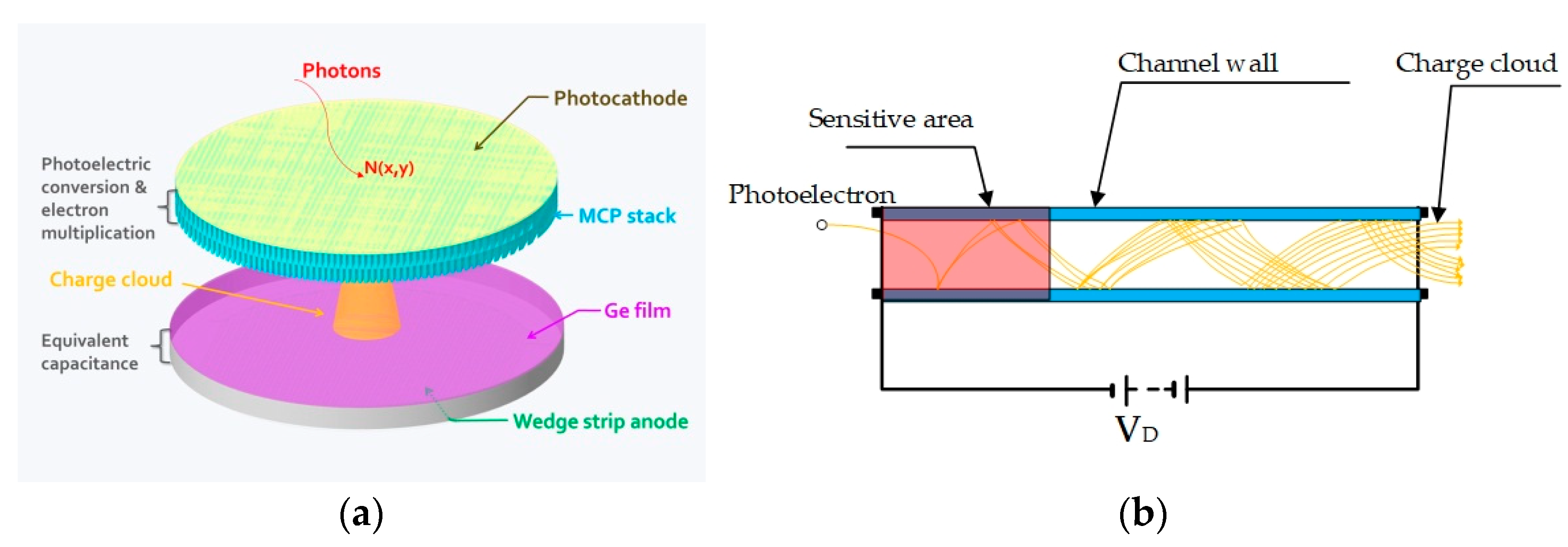
2.1. Protection for Detector

Our imaging detector, which we previously developed [25], utilizes an advanced microchannel plate to enhance image quality. The detector consists of a photocathode, a position-sensitive anode, and the microchannel plate, as illustrated in Figure 1a. The detector functions by converting weak light into photoelectrons through the photocathode, which are then multiplied by the V-type cascade microchannel plate to create an electron cloud. The multiplied electron cloud accelerates under the electric field and falls onto the sensitive anode, which is read by the analog front-end electronics. Then, the position decoding formula is applied to obtain the photon’s position, and photon counting is achieved. After a certain integration time, the gray image of the photon signal can be obtained.
The microchannel plate is a large array of two-dimensional distribution electron multiplier tube array. Each microchannel hollow tube can be considered a micro continuous amplification photomultiplier tube, as illustrated in Figure 1b. It is composed of leaded glass with a high quadratic emission coefficient. The current gain (μ) of MCP is usually determined via the ratio of channel length (L) to channel diameter (d), which can be approximated as:
μ = e δ × L d ,
where μ is the current gain of MCP and δ is the secondary electron emission coefficient of MCP channel wall, which is determined by channel material and electric field intensity.
If charged particles of space radiation penetrate the shielding layer and impact the inner wall of the microchannel plate at a certain energy and angle, secondary electrons will be excited in a manner similar to real photoelectrons. These secondary electrons then multiply and eventually form electron clouds at the output end, which can lead to false counts. As seen from Formula (1), the closer the position where the charged particles hit the inner wall of the microchannel plate is to the input end (as marked in red in Figure 1a), the larger the length-diameter ratio, the more times electron multiplication takes place, the higher the photoelectric pulse, and the easier it is for electronics to recognize it as a count. On the other hand, when the charged particles interact with the side wall of the microchannel plate near the output end, the length–diameter ratio will be relatively small and the gain will also decrease, potentially preventing it from being identified by electronics.
In Figure 2, the radiation protection structure of the detector is depicted. The detector is enveloped by an Al shell that provides electromagnetic shielding and acts as the first layer of radiation shielding. The optical system is connected to the front end of the detector, which only covers a portion of the detector’s total area and should not directly face the incident particles. A low-noise electronic readout circuit is connected to the front end, while the processing circuits can be placed at a slight distance. When illuminated from the side of the MCP, the diameter is equal to the thickness, resulting in an increase in the detection efficiency [26]. Consequently, a shielding ring is added to the side wall of the detector input end—the most sensitive area. The width of the shielding ring (Ws), shown in blue in Figure 2b, can be determined based on disturbance and weight constraints.

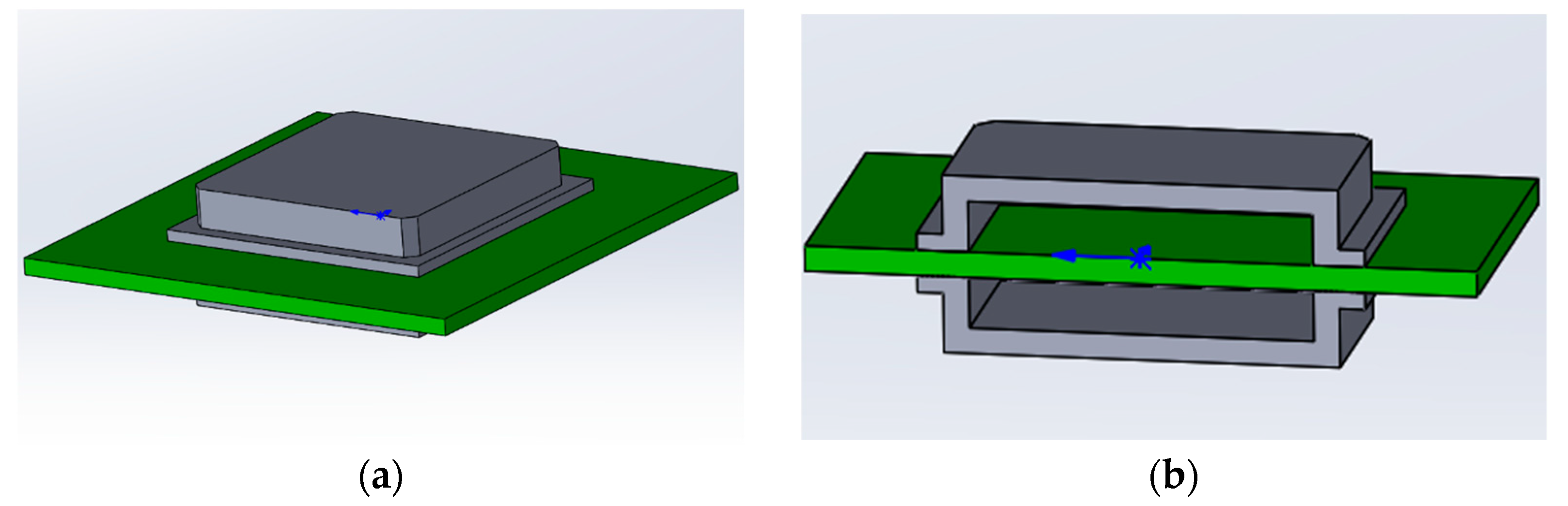
2.2. Local Protective Structure of Electronic Devices

Electronics are more focused on TID than on transient disturbances, which have been previously mentioned in regard to photon-counting detectors. A protective box is designed specifically for use with electronics in space, as illustrated in Figure 3. The box is composed of two separate boxes that enclose the sensitive electronic components and extend horizontally from the side walls, creating a finite boundary. Due to the design of the box, the equivalent thickness of the shield increases quickly when the incident angle is nearly parallel to the PCB, thus increasing the range of particles that can enter the PCB.
Figure 4 shows the geometrical dimensions of the outer edge of the protective box after optimization. The width of the edge is represented by D E , and its thickness is indicated by D T . The wall thickness of two local protective boxes on and off the PCB is denoted by D K . Whether the material is single or multi-layered, its equivalent density can be given by ρ e f f . The thickness of the PCB is marked as D P , and its equivalent density is described as ρ p . To ensure a uniform thickness in all directions, the width and thickness of the outer edge should abide by the following limits:
D E + D K 2 + D P 2 ρ e f f ρ p 2 × D K 2 ,
D T D K ρ p ρ e f f × D P ,
Here, the equivalent thickness of the PCB is noted as ρ p ρ e f f × D P . For any position on the top surface of the PCB, the width of the outer edge D E must be true in order for Equation (2) to be fulfilled. This ensures that the equivalent Al thickness of the path A length in the PCB is always greater than or equal to the side wall D K , as illustrated in Figure 4a. When the thickness of the outer edge D T is increased in order for Equation (3) to be true, then for any position on the top surface of the PCB, the equivalent Al thickness corresponding to the path B length from incident particles is always greater or equal to the side wall D K , as depicted in Figure 4b.
Since radiation can come from any angle, particles enter the substance from all directions at a 4π solid angle. The ray-tracing method was used to introduce multiple rays into the omnidirectional space from position O in order to be analyzed. As illustrated in Figure 5, the omnidirectional area is divided into several rooms with a small enough solid angle. The arrow on the ray OP marks the small space. The angle between the OP projection and the positive X axis in the XOY plane is denoted as φ (ranging from 0° to 360°), while the angle between the OP and XOY plane is defined as θ (−90° to +90°). With this information, the omnidirectional space radiation dose at point O of the device can be expressed as:
D O = 90 ° 90 ° 0 ° 360 ° D T φ , θ d φ d θ ,     φ ϵ 0 ° , 360 °   θ ϵ 90 ° , 90 ° ,
where T φ , θ represents the thickness of the shielding material penetrated by the ray. D T φ , θ indicates the radiation dose of the space corresponding to the ray OP through the shielding substance T φ , θ .
When the ray passes through the multilayer materials, the total shielding strength at this position can be given as follows:
S O = i = 1 n ρ φ , θ i × d φ , θ i ,     φ ϵ 0 ° , 360 °   θ ϵ 90 ° , 90 ° ,
where ρ φ , θ i is the density of the i-layer shielding material experienced in the range of φ , θ rays. d φ , θ i is the path length of the i-layer shielding material experienced in the range of φ , θ rays.
The angular resolution of the incident particle is preset to 10°, and multiple ray vectors are emitted into omnidirectional space based on a spherical coordinate system by selecting any origin in the PCB plane. When the ray vector intersects the structural model entity, it passes through the model and produces two points of intersection—one for the incoming ray and one for the outgoing ray. The (x, y, z) coordinates of both points are measured separately in order to obtain the Euclidean distance of each intersection pair. This distance is then calculated according to the coordinate values of all intersection pairs in order to determine the total path length of shielding material passed by the omni-directional rays at the origin.

2.3. Shielding Materials

Once charged particles enter a shielding material, they interact with the nuclei and electrons along their path, resulting in a gradual loss of energy. Depending on the degree of energy loss, the particles may either pass through the material, lose some energy, or become fully absorbed by it. When a proton interacts with a target substance, ionization and excitation occur due to inelastic collision with electrons. The resulting free electrons then interact with atoms based on their energy and direction. The energy loss rate due to ionization and excitation in a unit plane density can be calculated using the Bethe Formula (6) [27]. The energy lost by a proton in a unit path is referred to as the stopping power of the matter to the charged particle, or d E ρ d x .
d E ρ d x i o n = 4 π e 4 N 0 Z m v 2 A l n 2 m v 2 I 1 β 2 β 2 ,
where e denotes the Coulomb charge, N 0 is the Avogadro constant, Z represents the atomic number of the substance, m stands for the proton mass, v is the proton velocity, A is the atomic weight of the substance, I represents the average excitation energy of the substance atom, and β is the ratio of the proton velocity to the speed of light.
Unlike proton energy loss mechanisms, due to their large mass and small scattering angle, the path of protons in matter can be approximated as a straight line and bremsstrahlung energy loss can be disregarded. However, aside from ionization and excitation, bremsstrahlung radiation is produced when electrons interact with target materials. This is caused by the electron approaching the nucleus and interacting with its Coulomb field, resulting in energy being converted into radiation. The energy lost by radiation can be expressed as:
d E ρ d x r = 4 e 4 N 0 Z 2 E e 137 m 0 c 4 A l n 183 Z 1 / 3 + 1 18 ,
where m0 stands for the electron mass, c is the electron velocity, and E e represents the electron energy.
The ratio of radiation energy loss rate and ionization energy loss rate of electrons in a substance is approximately:
d E ρ d x r d E ρ d x i o n E e Z 700 ,
The total energy loss rate of the electron in the material is then given by:
d E ρ d x T = 4 e 4 N 0 Z 2 E e 137 m 0 c 4 A l n 183 Z 1 / 3 + 1 18 1 + 700 E e Z ,
Formula (6) shows that the amount of energy protons lose is inversely proportional to the square of their velocity. The rate of energy loss starts increasing before the proton comes to a complete stop. As the proton’s energy decreases, the cross-section of interaction increases, resulting in more energy deposition. Therefore, this mechanism dominates before the proton stops completely, and almost all of the energy is deposited near the slice of material at the end of the range. The range in the material increases exponentially with an increase in proton energy. Hence, a shielding material with enough thickness is required to prevent high-energy protons from penetrating.
Formula (9) shows that the energy loss rate of electrons is proportional to the energy of the electron, with more energy lost at the beginning of the range. As electrons lose energy, their velocity decreases, leading to an increase in interaction cross-section and more energy deposition. With more energy lost, electrons have less energy deposition. Therefore, two conflicting processes produce maximum energy deposition at the front end of the range. The range in the material increases nearly linearly with an increase in electron energy. A shielding material with a certain thickness can attenuate most of the electron energy.
The energy loss rate of protons and electrons per unit length of material is approximately proportional to Z/A, but electrons are also subject to the elastic scattering of nuclei, equivalent to increasing shielding thickness. The energy loss rate of elastic scattering is proportional to Z2/A. Table 1 shows the three commonly used material properties. Al has a greater Z/A than Ta, which means that Al shields protons better than Ta, while for electrons, Ta shields electrons better than Al due to elastic scattering. As shown in Formula (9), bremsstrahlung increases rapidly with an increase in incident electron energy. A material with a high atomic number, such as Ta, can attenuate more energy of high-energy electrons, but the proportion of X-ray energy brought by bremsstrahlung is also significant. Secondary radiation decreases the initial attenuation effect. HDPE has a lower atomic number than aluminum, which means it interacts less strongly with electrons and protons. This can be beneficial in certain situations, as HDPE can more effectively attenuate the energy of electrons and protons and scatter electrons away from the protected area. This also means that less mass is required for HDPE to achieve the same shielding capability as aluminum. Additionally, HDPE is a good insulator, which can help prevent electrical discharge in the high-voltage environments of photodetectors.
Because the energy distribution of charged particles in space is continuous, a single-layer material is not sufficient for effectively shielding the charged particles of all energies. To achieve better shielding results for different types and energies of charged particles, it is necessary to use combinations of multi-layer materials.

3. Results and Discussion

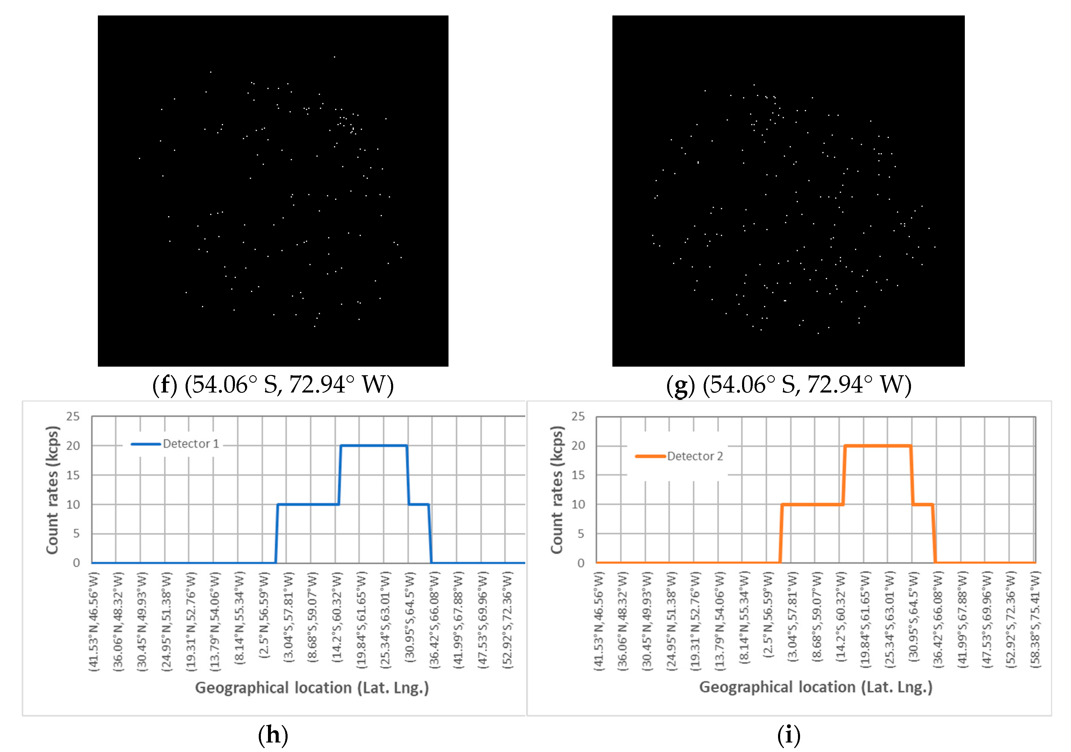
3.1. Test of Photon Counting Imaging in Space

Our Wide-angle Aurora Imager has been in orbit for over six years. The detector utilizes the photon counting detector described in this paper, although it adopts more conventional Al shielding measures. Instead of a local protective box, the electronics box uses an overall Al thickening measure. So far, no changes to the function or performance of electronic devices due to TID have been noticed. To observe the transient disturbance of charged particles on the detector, a dark background test was performed within the SAA region.
Figure 6 presents six dark background images taken by two sets of photon-counting imaging detectors before and after the FY-3D satellite passed through the SAA. Further information regarding the scientific instrument can be found in our previously published articles [20,21]. The dark background images were taken in the absence of incident photons, which determines the detection system’s lower limit of dynamic range. The images were captured at a latitude and longitude of (14.26° N, 53.95° W) prior to the satellite entering the SAA region, as seen in Figure 6b,c. The exposures were 50, and the dark count rates ranged from 0 to 10 kcps. However, the dark count rates increased drastically when the satellite was in the SAA region, reaching a range of 10 kcps to 20 kcps, as displayed in Figure 6h, due to the radiation effect of the high-energy charged particles.
Figure 6d,e depicts a single-exposure image taken at (20.42° S, 61.79° W). The number of bright spots in the image increased significantly, with even the presence of irregular bright lines. Correspondingly, Figure 6f,g shows images obtained from the satellite at (54.06° S, 72.94° W) after it passed through the SAA region. There were also 50 exposures, and the dark count rates decreased back to their original levels before entering the SAA region, as shown in Figure 6h.
In order to improve the quantum efficiency and the electron gain of detectors, materials with lower work functions are usually implemented for the photocathode of the incident window of the detector and the aperture of the microchannel plate. When the satellite enters the SAA region, high-energy charged particles are able to penetrate the protective structure of the detection system. These particles interact with the photocathode or the aperture wall of the microchannel plate and produce secondary electrons. After the secondary electrons have been multiplied, they are output to the detector anode under the influence of an electric field. This, in turn, is followed by an electronic circuit that converts the electrons into voltage pulses. The discriminator can recognize and count such pulses, leading to an increase in the dark count. When the instrument is removed from the SAA region, high-energy charged particles in space will return to a normal distribution, and the dark count of the system will fall back to its typical level.
We should remain vigilant to large increases in particle flux in the SAA region caused by high solar activity years or other space events. If the dark count rates were to approach the system’s maximum or drop drastically, it would be necessary to reduce or turn off the high-voltage power supply of the detection system and pause operations while the instrument enters the SAA. This is only a makeshift measure though, and to properly tackle this issue, more effective shielding measures against charged particles need to be implemented.
Unlike electronics, instantaneous radiation has a significant effect on detectors. In addition, the quantum efficiency and spectral response characteristic of the photocathode is altered due to changes in its chemical properties as the total radiation dose increases, and the electron gain of the microchannel plate is also reduced. In the long-term, both detectors and electronic devices will suffer a decrease in their lifetimes because of radiation.

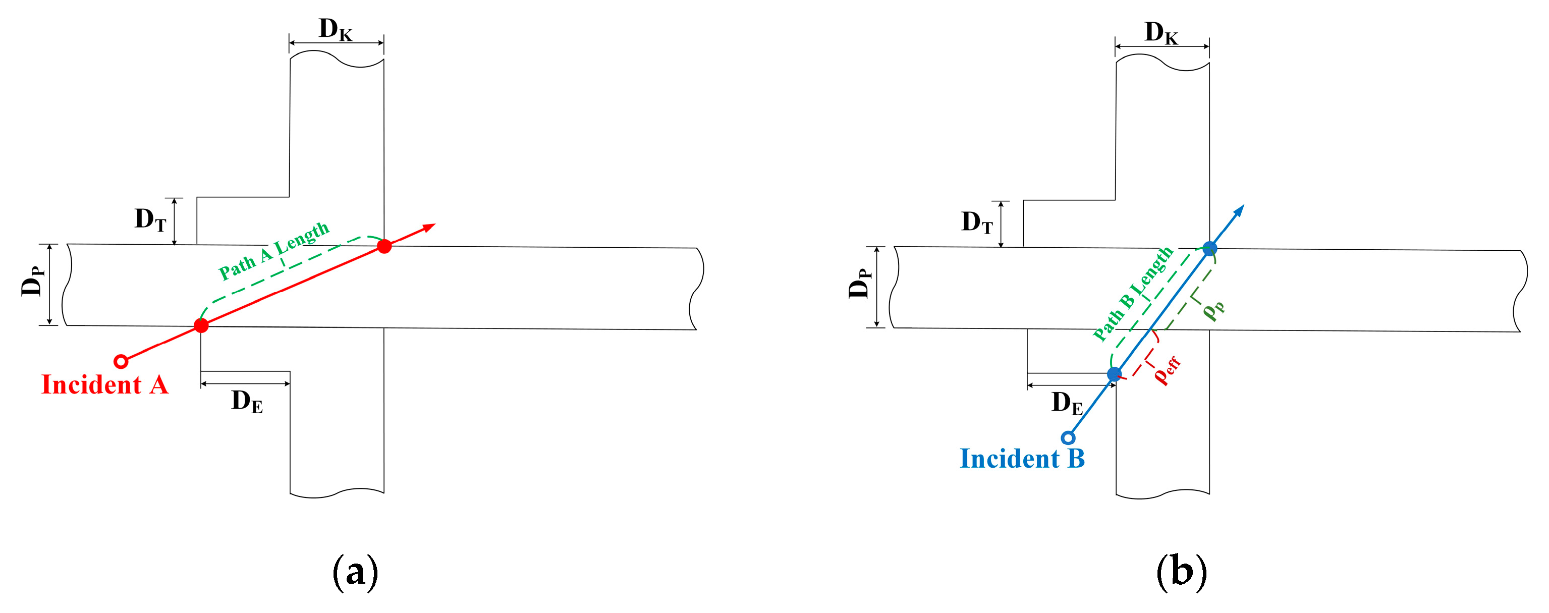
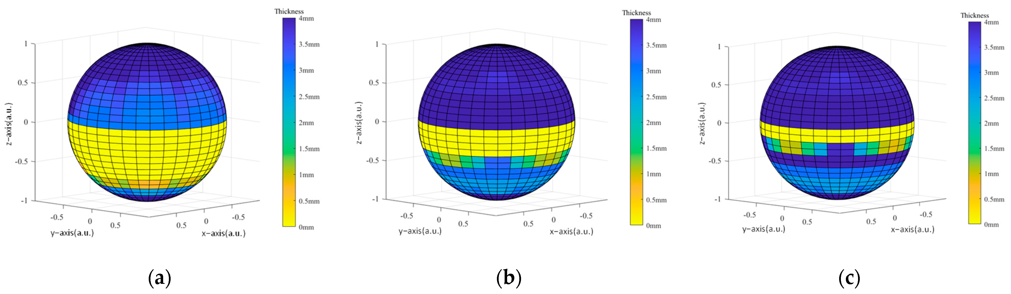
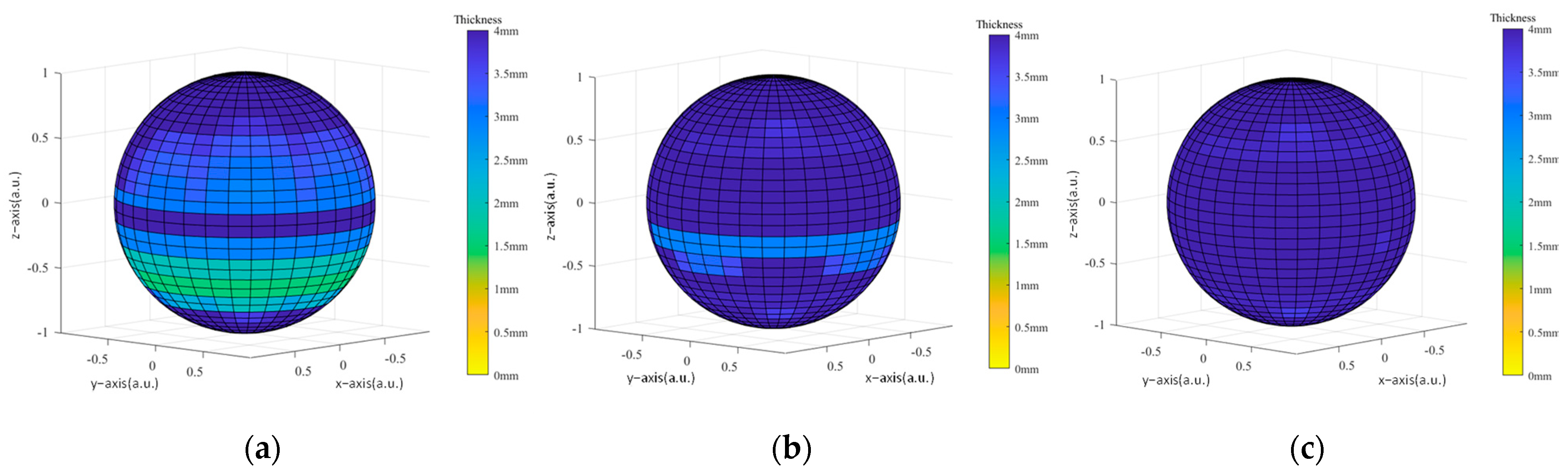
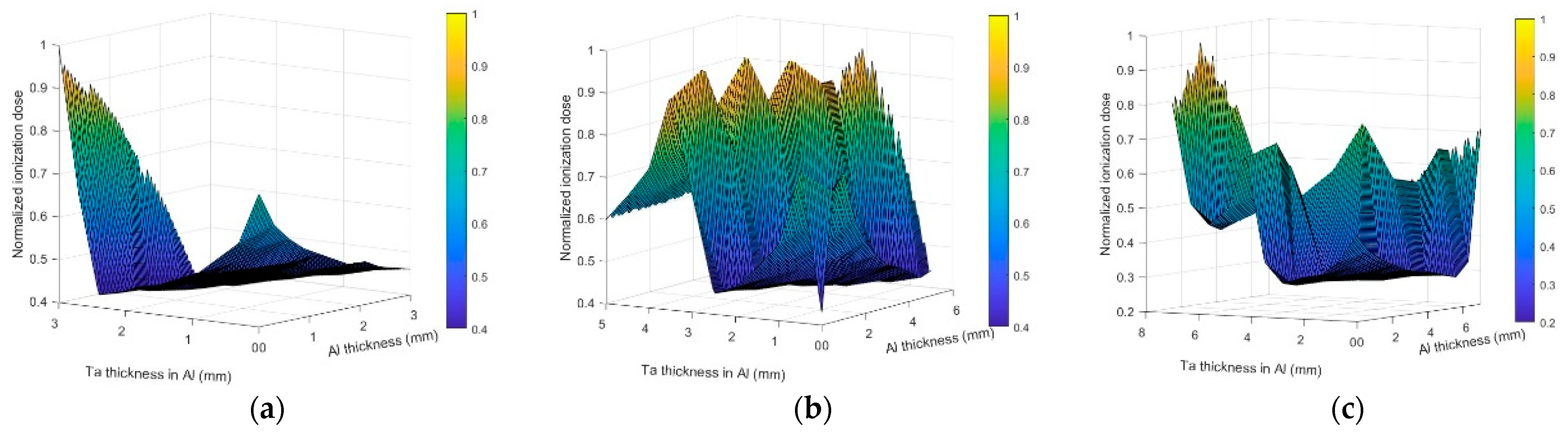
3.2. Uniformity of Protection

Since the protective measures outlined in this paper are intended to be implemented on an upgraded instrument, real-life orbit verification has not yet been conducted. As a result, we have relied on structural modeling and material simulation analysis to achieve our verification goals.
This paper takes a specific model as an example to analyze the omnidirectional shielding thickness for the edge devices on the top surface of a PCB in a local protective box. FR4 epoxy board was selected as the board’s substrate, with a PCB density recorded as 0.93 g/cm3 due to the multi-layer structure, PP adhesive, aperture, and copper. Three widths of the outer edge D E were used for calculation: 0, 3 mm and 6 mm. Specific parameters are shown in Table 2.
A spherical color temperature diagram can be used to represent the calculation result of the path length of an omnidirectional ray. Path lengths over 4 mm are indicated with the same color to distinguish the weak area of radiation protection more clearly, as shown in Figure 7. When PCB protection or the outer edge of the box are not taken into account, the lower half space of the edge points will appear as weak areas, that is, the zenith angle in the range of 100° to 140°. The protective thickness is less than 0.5 mm, accounting for more than 1/4 of the total 4π omnidirectional space. When the width of the outer edge D E increases to 3 mm and 6 mm, the proportion of space area with a protective thickness less than 0.5 mm decreases significantly. The weak area eventually tends to be close to the parallel direction of the PCB.
Furthermore, when considering the protective factors of the PCB at a zenith angle of 100°, as illustrated in Figure 8, the range of particles within the PCB can reach over 17 mm, which is equal to a 5 mm thick Al layer. The worst position of the protective thickness occurs when the zenith angle is equal to 130°, where the equivalent Al thickness would be only about 1.5 mm, even with PCB protection. To offset the incident range of particles in the zenith angle range of 110°–140°, the outer edge of the boundary should be increased. This would equate to an equivalent Al thickness of 4 mm with a 6 mm wide outer edge. Additionally, the protective thickness over the whole 4π omnidirectional space can exceed 3 mm.
In cases of extreme weight constraints, the width of the outer edge can be designed at 3 mm. This results in protective thickness, which is relatively uniform in the overall space, with the weak area being reduced to 2.9 mm only when the zenith angle is approximately 110°. The outer edge of the enclosure should be combined with the range of particles in the PCB. It is important to maintain radiation protection while minimizing the size of the outer edge to keep the overall weight of the protective box as low as possible.
Due to the high sensitivity of the photon-counting imaging detector mentioned in Section 2.1, an outer edge structure may also be considered in order to provide protection for the detector inlet. As the exposed area of the peripheral wall of the detector is dominant, applying three layers of materials, as mentioned in Section 3.2, would be beneficial in these areas to prevent charged particles from penetrating too far, thus improving the sensitivity of the detection system.

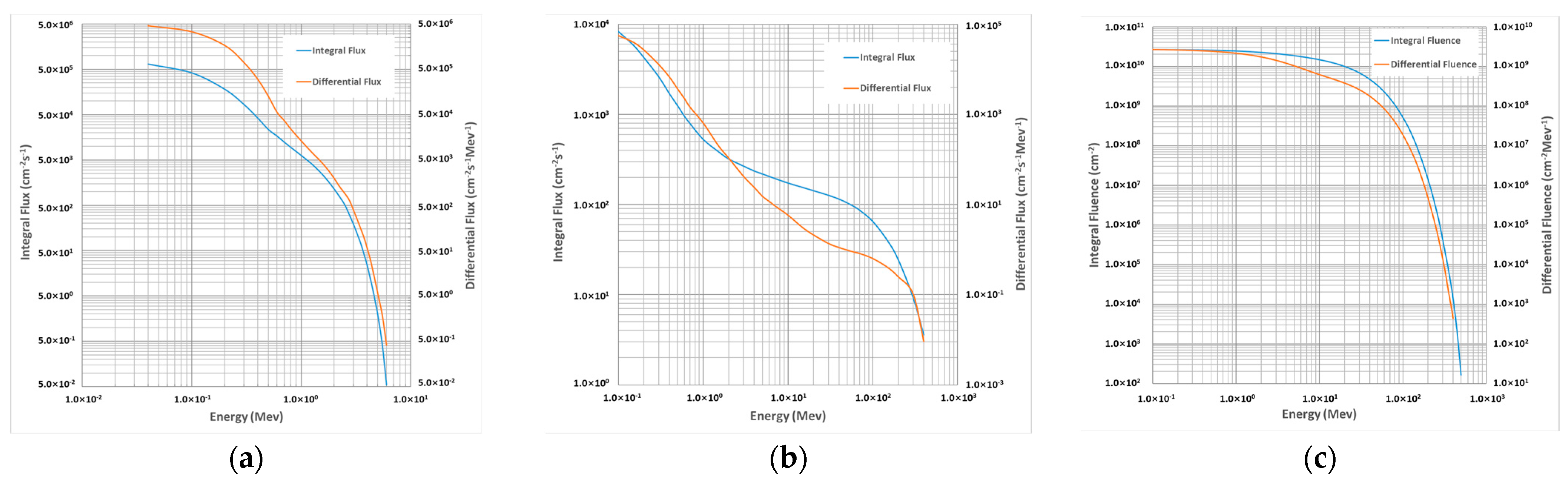
3.3. Simulation of Multilayer Shield

Taking the particle environment of the FY-3 satellite’s orbit as input, the flux of electrons and protons in the radiation belt and the solar proton fluence can be used as a planar source. The AE-8 MAX and AP-8 MAX models, developed by the NSSDC of the United States, are used to determine the electron and proton beams of the Earth’s radiation belt, respectively. Additionally, NSSDC’s King model (95% confidence) is used for solar proton fluence. This paper computes the radiation dose received by the satellite’s position over an 8-year mission, with orbital parameters provided in Table 3.
As depicted in Figure 9a, the electron flux distribution in the radiation belt showcases an energy range from 0.04 MeV to 6 MeV, with flux concentration in energies less than 3 MeV. Similarly, Figure 9b illustrates the proton flux distribution within the same zone, where the energy range is mainly between 0.1 MeV and 300 MeV, with flux intensity primarily below 100 MeV. Lastly, Figure 9c elucidates the solar proton fluence distribution, featuring an energy range predominantly between 0.1 MeV and 500 MeV, with high fluence concentration in values lower than 50 MeV.
The multi-layer shielding materials have a three-layer planar geometry consisting of Al, Ta, and HDPE arranged in sequence (Al-Ta-HDPE). The distance between the object and the shielding layer is 5 mm, and the object thickness is chosen for typical 0.1 mm semiconductor silicon wafers used in the device. The total equivalent Al thickness for the shielding materials was selected as 3 mm, 5 mm, and 7 mm, and the shielding calculation results for the three materials with different thickness ratios are shown in Figure 10. When the equivalent Al thicknesses of Al, Ta, and HDPE are 0.7 mm, 2.8 mm, and 3.5 mm, respectively, the total equivalent Al thickness is 7 mm, yielding the lowest TID in the object, which is 71% lower than the maximum dose. However, for total equivalent Al thicknesses of 3 mm or 5 mm, even if the three materials reach the best mass ratio, the lowest ionization dose in the object is only 57 % lower than the highest dose.
Under the same mass, different combinations of materials can yield different shielding results. Simulation analysis can estimate the better shielding effect of some materials with different thickness components. Even with the same mass ratio of three materials, the ionization dose trends obtained in the object differ. The relative thickness of shielding materials varies dynamically with the energy of incident particles. When the energy is large, the thickness of shielding material will be relatively small, which is not enough to completely attenuate the electron energy. In such cases, Ta has better shielding results than Al and HDPE. When the incident energy is small, the thickness of shielding materials will be comparatively large, which can completely block the incident electrons. However, bremsstrahlung produces X-rays that contribute significantly to the ionizing dose in the object, making the combination of appropriate shielding materials relatively effective.
We conducted a comprehensive evaluation of the photon-counting imaging system, analyzing its sensitivity, maximum counting rates, and dark counts under various shielding conditions. The sensitivity and maximum counting rates are dependent on the quantum efficiency of the detector, the gain, and the system’s response time. Our results, presented in Table 4, indicate that a local shield does not affect sensitivity or maximum counting rates since it does not obstruct the inlet light. To determine the effectiveness of the shielding ring proposed in Section 2.1, we simulated the changes in dark count rates under three conditions: multi-layer material as a whole, local shielding, and single-layer Al shielding. The materials used in the shielding layer, from outside to inside, were Al, Ta, and HDPE. Our results showed that the local shielding ring achieved the same radiation protection effect as the global shielding while reducing the weight requirement. However, the single-layer Al shielding scheme had a weaker radiation protection effect than the previous two, due to the simulation’s use of an omnidirectional uniform radiation model. This resulted in charged particles being able to penetrate the Al layer more easily, causing more electron multiplication at the detector input.

4. Conclusions

Charged particle radiation can have short and long-term effects on a photoelectric detection system. In particular, photon-counting imaging detectors are highly sensitive to transient charged particles, leading to an increase in dark noise. To block charged particles, the most sensitive area of the detector’s input side wall requires an additional shielding ring. To reduce TID damage to electronic devices, the protective structure’s geometry is crucial. By including the outer edge of the finite boundary and considering the non-metallic structure’s equivalent thickness, which refers to the particle’s range in the PCB, the all-directional protection of every point is achieved. In addition to the protective structure’s geometry, selecting appropriate shielding materials is also crucial. Charged particles have a broad energy distribution and penetrate shielding materials differently depending on their range. Multilayer materials provide superior shielding results compared to monolayer materials. Adjusting the mass ratio of different materials can determine optimal shielding strategies with the same mass. It is important to consider the equipment’s particle environment in orbit in order to choose the right shielding material and mass ratio combination.
Further research will be conducted on the shielding properties of materials such as aluminum alloy and boron-polyethylene, which are suitable for aerospace applications due to their toughness and thermal stability. The installation of shielding materials and their distance from protected objects will also be studied in order to improve shielding effect and reliability. Based on these strategies, a photoelectric detection instrument is being considered for the next generation of Fengyun satellites.

5. Patents

The method of radiation protection for electronic equipment in space was patented by the State Intellectual Property Office of China on 9 October 2022.

Author Contributions

Conceptualization, Z.-W.H. and K.-F.S.; methodology, Z.-W.H.; software, Z.-W.H.; validation, Z.-W.H., K.-F.S. and H.-J.Z.; formal analysis, Z.-W.H.; investigation, L.-P.H.; resources, Q.-F.G.; data curation, G.-X.D. and H.-J.Z.; writing—original draft preparation, Z.-W.H.; writing—review and editing, C.-W.L. and Y.L.; visualization, Q.-F.G.; supervision, B.C.; project administration, S.-J.L.; funding acquisition, L.-P.H. All authors have read and agreed to the published version of the manuscript.

Funding

This research was funded by the National Key Research and Development Program of China, grant number 2022YFF0708500.

Institutional Review Board Statement

Not applicable.

Informed Consent Statement

Not applicable.

Data Availability Statement

Any logical additional data requests may be sent to Z.-W.H.

Conflicts of Interest

The authors declare no conflict of interest.

References

  1. Bourdarie, S.; Xapsos, M. The near-earth space radiation environment. IEEE Trans. Nucl. Sci. 2008, 55, 1810–1832. [Google Scholar] [CrossRef]
  2. Ripoll, J.F.; Claudepierre, S.G.; Ukhorskiy, A.Y.; Colpitts, C.; Li, X.; Fennell, J.F.; Crabtree, C. Particle dynamics in the Earth’s radiation belts: Review of current research and open questions. J. Geophys. Res. Space Phys. 2020, 125, e2019JA026735. [Google Scholar] [CrossRef]
  3. Anderson, P.C.; Rich, F.J.; Borisov, S. Mapping the South Atlantic Anomaly continuously over 27 years. J. Atmos. Sol. Terr. Phys. 2018, 177, 237–246. [Google Scholar] [CrossRef]
  4. Heirtzler, J.R. The future of the South Atlantic anomaly and implications for radiation damage in space. J. Atmos. Sol. Terr. Phys. 2002, 64, 1701–1708. [Google Scholar] [CrossRef]
  5. Topper, A.D.; Casey, M.C.; Wilcox, E.P.; Campola, M.J.; Cochran, D.J.; O’Bryan, M.V.; Pellish, J.A.; Majewicz, P.J. Compendium of Radiation Effects Test Results from NASA Goddard Space Flight Center. In Proceedings of the Nuclear and Space Radiation Effects Conference (NSREC), Ottawa, ON, Canada, 17–23 July 2021. [Google Scholar]
  6. Rahman, M.M.; Shankar, D.; Santra, S. Analysis of radiation environment and its effect on spacecraft in different orbits. In Proceedings of the International Astronautical Congress (IAC2017), Adelaide, Australia, 25–29 September 2017. [Google Scholar]
  7. Ferraro, R.; Alía, R.G.; Danzeca, S.; Masi, A. Analysis of Bipolar Integrated Circuit Degradation Mechanisms Against Combined TID–DD Effects. IEEE Trans. Nucl. Sci. 2021, 68, 1585–1593. [Google Scholar] [CrossRef]
  8. Marcelot, O.; Goiffon, V.; Raine, M.; Duhamel, O. Radiation effects in CCD on CMOS devices: First analysis of TID and DDD effects. IEEE Trans. Nucl. Sci. 2015, 62, 2965–2970. [Google Scholar] [CrossRef]
  9. Samwel, S.W.; El-Aziz, E.A.; Garrett, H.B.; Hady, A.A.; Ibrahim, M.; Amin, M.Y. Space radiation impact on smallsats during maximum and minimum solar activity. Adv. Space Res. 2019, 64, 239–251. [Google Scholar] [CrossRef]
  10. Morton, T.; Lyons, V. Estimation of the radiation environment based on the NASA AP-8 and AE-8 Models. In Proceedings of the 5th International Workshop on Radiation Effects on Semiconductor Devices for Space Applications, Dushanbe, Tajikistan, 1 October 2002. [Google Scholar]
  11. Chunqin, W.; Yueqiang, S.; Guangwei, C.; Zhang, X.; Li, J.; Zhang, X.; Jing, T.; Shen, G.; Zhang, S.; Huang, C.; et al. Radiation dose evaluation and analysis inside FY-3A satellite. Chin. J. Space. Sci. 2015, 35, 56–63. (In Chinese) [Google Scholar]
  12. Wang, C.Q.; Zhang, X.G.; Shen, G.H.; Zhang, S.; Zhang, X.; Huang, C.; Li, X. Dynamic results of electron flux in radiation belt from 2011 to 2015 based on FY-3B satellite observation. Chin. J. Geophys. 2021, 64, 1831–1841. [Google Scholar]
  13. Cepeda-Rizo, J.; Gayle, J.; Ravich, J. Thermal and Structural Electronic Packaging Analysis for Space and Extreme Environments, 1st ed.; CRC Press: Boca Raton, FL, USA, 2022. [Google Scholar]
  14. Dacko, A.; Kowalski, T.; Baran, J.; Barciński, T. Electronic box structural analyses for a space flight. In Photonics Applications in Astronomy, Communications, Industry, and High-Energy Physics Experiments, Proceedings of the Wilga 2019—Photonics Applications and Web Engineering, Wilga, Poland, 6 November 2019; SPIE: Paris, France, 2019. [Google Scholar]
  15. Fenske, M.T.; Barth, J.L.; Didion, J.R.; Mule, P.; The Development of Lightweight Electronics Enclosures for Space Applications. NASA Technical Reports Server. Available online: https://ntrs.nasa.gov/citations/20030022659 (accessed on 26 January 2023).
  16. Daneshvar, H.; Milan, K.G.; Sadr, A.; Sedighy, S.H.; Malekie, S.; Mosayebi, A. Multilayer radiation shield for satellite electronic components protection. Sci. Rep. 2021, 11, 20657. [Google Scholar] [CrossRef] [PubMed]
  17. Fetzer, A. Radiation Shielding Simulations for Small Satellites on Geostationary Transfer Orbit. Master’s Thesis, Aalto University, Espoo, Finland, 25 April 2022. [Google Scholar]
  18. Chen, B.; Song, K.F.; Li, Z.H.; Wu, Q.-W.; Ni, Q.-L.; Wang, X.-D.; Xie, J.-J.; Liu, S.-J.; He, L.-P.; He, F. Development and calibration of the Moon-based EUV camera for Chang’e-3. Res. Astron. Astrophys. 2014, 12, 1654–1663. [Google Scholar] [CrossRef]
  19. Yan, Y.; Wang, H.N.; He, H.; He, F.; Chen, B.; Feng, J.-Q.; Ping, J.-S.; Shen, C.; Xu, R.-L.; Zhang, X.-X. Analysis of observational data from Extreme Ultra-Violet Camera onboard Chang’E-3 mission. Astrophys. Space Sci. 2016, 361, 76. [Google Scholar] [CrossRef]
  20. Zhang, X.X.; Chen, B.; He, F.; Song, K.; He, L.; Liu, S.; Guo, Q.; Li, J.; Wang, X.; Zhang, H.; et al. Wide-field auroral imager onboard the Fengyun satellite. Light. Sci. Appl. 2019, 8, 47. [Google Scholar] [CrossRef] [PubMed]
  21. Ding, G.; Li, J.; Zhang, X.; He, F.; He, L.; Song, K.; Sun, L.; Dai, S.; Liu, S.; Chen, B.; et al. Wide-field aurora imager onboard Fengyun satellite: Data products and validation. Earth Planet. Phys. 2021, 5, 73–78. [Google Scholar] [CrossRef]
  22. Chen, B.; Zhang, X.X.; He, L.P.; Song, K.; Liu, S.; Ding, G.; Dun, J.; Li, J.; Li, Z.; Guo, Q.; et al. Solar X-ray and EUV imager on board the FY-3E satellite. Light. Sci. Appl. 2022, 11, 329. [Google Scholar] [CrossRef] [PubMed]
  23. Allison, J.; Amako, K.; Apostolakis, J.; Arce, P.; Asai, M.; Aso, T.; Bagli, E.; Bagulya, A.; Banerjee, S.; Barrand, G.; et al. Recent developments in Geant4. Nucl. Instrum. Methods Phys. Res. A 2016, 835, 186–225. [Google Scholar] [CrossRef]
  24. Kalospyros, S.A.; Gika, V.; Nikitaki, Z.; Kalamara, A.; Kyriakou, L.; Emfietzoglou, D.; Kokkoris, M.; Georgakilas, A.G. Monte Carlo Simulation-Based Calculations of Complex DNA Damage for Incidents of Environmental Ionizing Radiation Exposure. Appl. Sci. 2021, 11, 8985. [Google Scholar] [CrossRef]
  25. Han, Z.W.; Song, K.F.; Zhang, H.J.; Yu, M.; He, L.; Guo, Q.; Wang, X.; Liu, Y.; Chen, B. Photon Counting Imaging with Low Noise and a Wide Dynamic Range for Aurora Observations. Sensors 2020, 20, 5958. [Google Scholar] [CrossRef] [PubMed]
  26. Tulej, M.; Meyer, S.; Lüthi, M.; Lasi, D.; Galli, A.; Piazza, D.; Desorgher, L.; Reggiani, D.; Hajdas, W.; Karlsson, S.; et al. Experimental investigation of the radiation shielding efficiency of a MCP detector in the radiation environment near Jupiter’s moon Europa. Nucl. Instrum. Methods Phys. Res. Sect. B 2016, 383, 21–37. [Google Scholar] [CrossRef]
  27. Sigmund, P. Particle Penetration and Radiation Effects; Springer Series in Solid-State Sciences; Springer: Berlin/Heidelberg, Germany, 2014; Volume 2, p. 179. [Google Scholar]
Figure 1. Schematic structure of a photon counting imaging detector. (a) Principle of imaging detectors; (b) single channel section of MCP.
Applsci 13 05905 g001
Figure 2. (a) The structure of detector assemblies; (b) profile of an imaging detector module.
Applsci 13 05905 g002
Figure 3. Model of local protective structure with finite boundary. (a) Overall view of the box; (b) sectional view of the box.
Applsci 13 05905 g003
Figure 4. Path diagram of incident particles where two ultimate angles, incidents A and B. (a) The length of the red line between the two solid intersections represents the path A length in the PCB; (b) path B of the blue line is divided into two lengths, namely the path in material density ρ e f f and the path in material density ρ p .
Applsci 13 05905 g004
Figure 5. Angle representation of ray tracing. The red arrow line represents one of several rays.
Applsci 13 05905 g005
Figure 6. Dark background images before and after the Wide-angle Aurora Imager passed through the SAA. (a) The image was captured by the Doris instrument aboard the Jason−1 satellite and shows the South Atlantic Anomaly (SAA)—a region close to Earth where the planet’s magnetic field is relatively weaker compared to an idealized Earth-centered dipole field. As a result, this region experiences an elevated flux of energetic particles, which exposes orbiting satellites to higher levels of radiation than usual. The colors on the image, ranging from green to red, represent the increasing flux of charged particles in the SAA, as the Earth’s magnetic field weakens in this region; (b,c) exposure numbered 50 instances, with each exposure time 0.34 s; (d,e) exposure numbered one instance, with a time of 0.34 s; (f,g) exposure numbered 50 instances, with each exposure time 0.34 s; (h,i) dark count rates of the two detectors corresponding to the trajectory in Figure 6a. The counting rate curves of detector one and detector two overlap completely, as the counting rate statistics of the instrument are based on a fixed set of blocks. The curves accurately represent the continuous measurements made in orbit and are based on real data points.
Applsci 13 05905 g006aApplsci 13 05905 g006b
Figure 7. Omnidirectional protection thickness in the absence of PCB protection. (a)   D E = 0 mm; (b)   D E = 3 mm; (c   D E = 6 mm.
Applsci 13 05905 g007
Figure 8. Omnidirectional protection thickness with PCB. (a)   D E = 0 mm; (b)   D E = 3 mm; (c)   D E = 6 mm.
Applsci 13 05905 g008
Figure 9. Particle environment in the orbit of the FY-3 satellite. The horizontal axis represents the energy of incident particles, while the main vertical axis shows the integral flux of omnidirectional particles. Additionally, the secondary vertical axis displays the differential flux of particles. The particle flux density per unit energy is a measure of the number of radiant energy particles that impinge on a surface over a given period of time, divided by the product of the surface area, characteristic energy of the particles, and the time interval. (a) Electron flux distribution in the radiation belt; (b) proton flux distribution in the radiation belt; (c) solar proton fluence distribution.
Applsci 13 05905 g009
Figure 10. Ionization dose of various particles predicted by the FY-3 satellite orbit after multilayer shielding. At a certain total thickness, TID was obtained by different thickness ratios of three materials. The X and Y coordinates represent the equivalent aluminum thickness of Ta and Al thickness, respectively, while the remaining equivalent aluminum thickness is assigned to HDPE. To facilitate comparison and comprehension, the maximum TID is used as a normalization benchmark. It is evident from the figure that TID is significantly different for the various proportions of Al, Ta, and HDPE under the same weight. (a) The total thickness is 3 mm; (b) the total thickness is 5 mm; (c) the total thickness is 7 mm.
Applsci 13 05905 g010
Table 1. Parameters of three materials.
MaterialsDensityAtomic Number (Z)Atomic Weight (A)Z/A
Aluminum (Al)2.7 g/cm31326.98 g/mol0.48
High-Density Polyethylene (HDPE)0.95 g/cm32.25**
Tantalum (Ta)16.6 g/cm373180.95 g/mol0.40
* The atomic weight of polyethylene cannot be defined as it is a polymer composed of repeating units of ethylene monomer (C2H4).
Table 2. Parameters of the protective box.
Group D K D P D T D E ρ e f f ρ p
13 mm3 mm2 mm0 mm2.8 g/cm30.93 g/cm3
23 mm3 mm2 mm3 mm2.8 g/cm30.93 g/cm3
33 mm3 mm2 mm6 mm2.8 g/cm30.93 g/cm3
Table 3. Orbital parameters of FY-3 satellite.
IndexParameters
CategoriesNPSSO
Orbital altitude836.0 km
Orbital inclination98.75°
Orbital eccentricity≤0.0025
Orbital period101.5 min
Longitude of ascending node14:00 PM
Table 4. Performance analysis of various shielding configurations.
Shielding ConfigurationsSensitivityMaximum
Counting Rates
Dark Count Rates
Whole shielding with three layers8.79 count s−1 Rayleigh−1350 kcps0.068 *
Local shielding with three layers8.78 count s−1 Rayleigh−1351 kcps0.079 *
Single-layer shielding using aluminum8.80 count s−1 Rayleigh−1350 kcps1 *
* The results were normalized using the performance data obtained with single-layer aluminum shielding as a reference.
Disclaimer/Publisher’s Note: The statements, opinions and data contained in all publications are solely those of the individual author(s) and contributor(s) and not of MDPI and/or the editor(s). MDPI and/or the editor(s) disclaim responsibility for any injury to people or property resulting from any ideas, methods, instructions or products referred to in the content.

