
Interferences of Electromagnetic Pulses on Microcontroller Units


Abstract
:1. Introduction
2. Experimental Environment
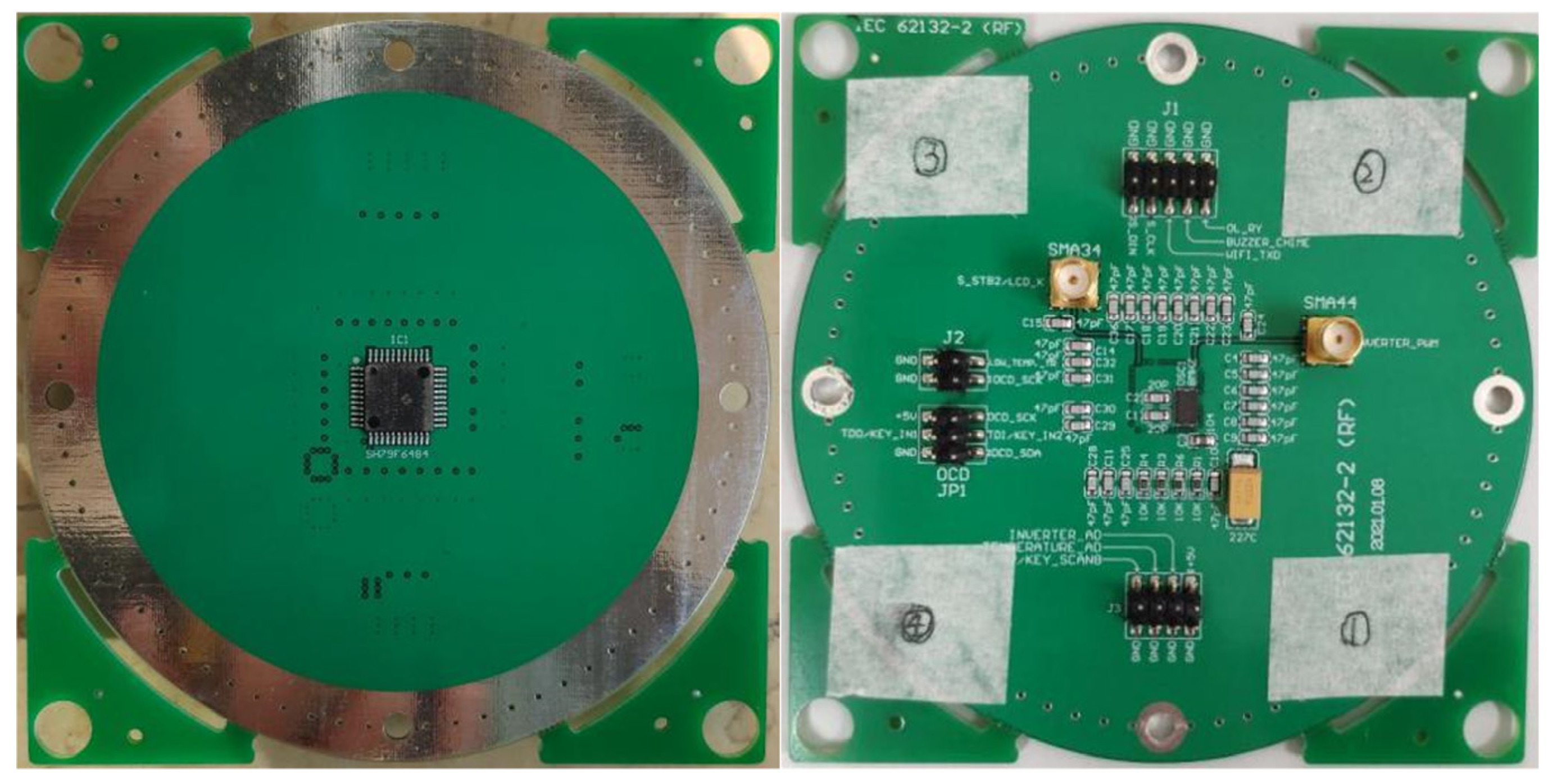
2.1. MCU
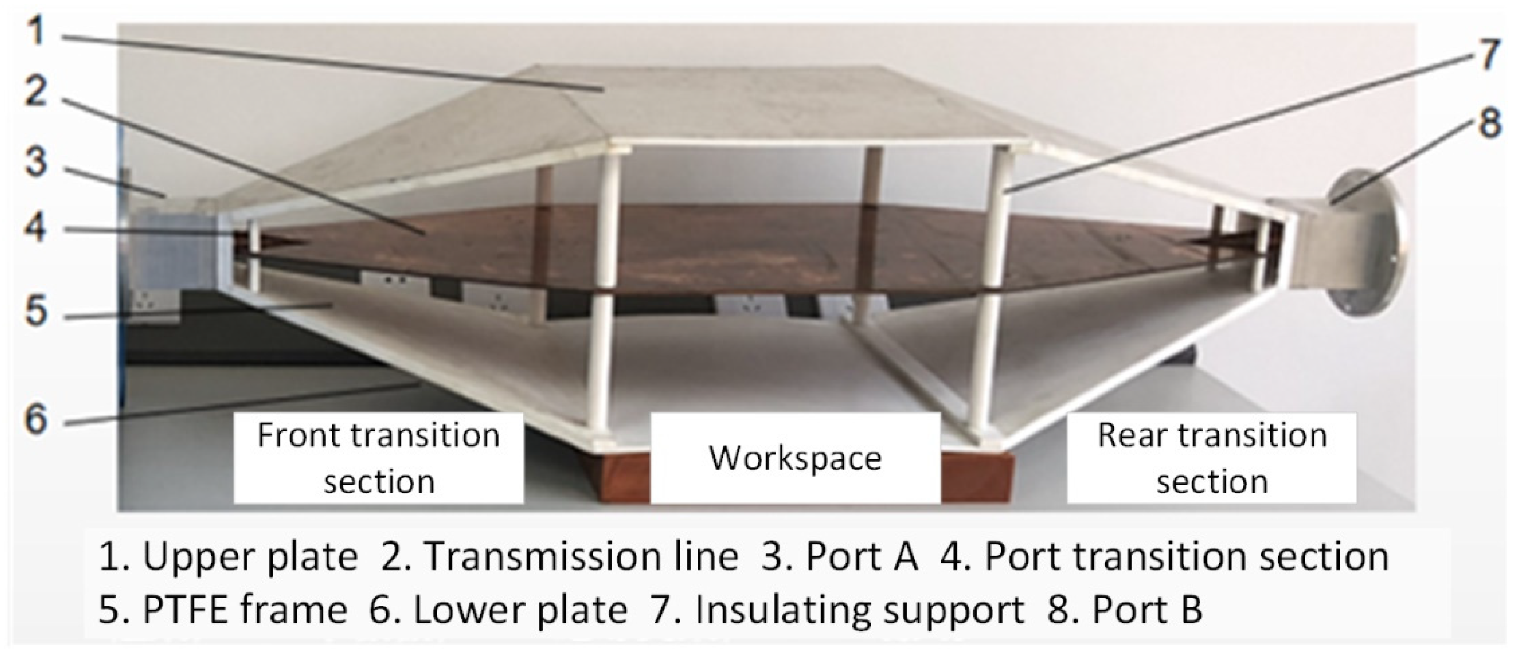
2.2. EMP Simulator
3. Experimental Protocol
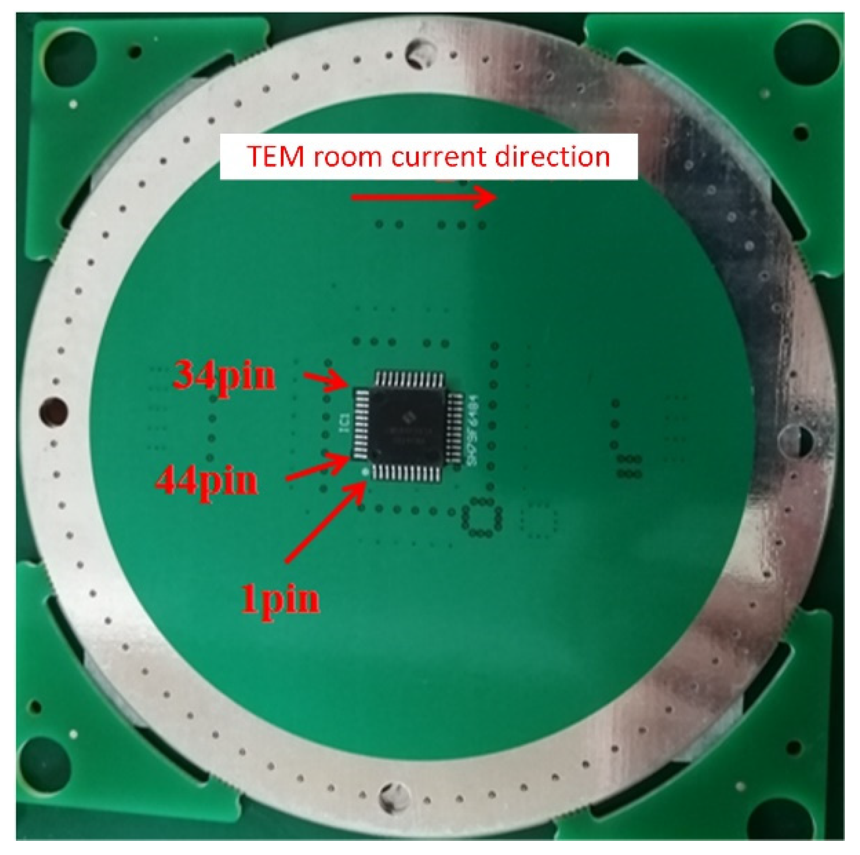
- (1)
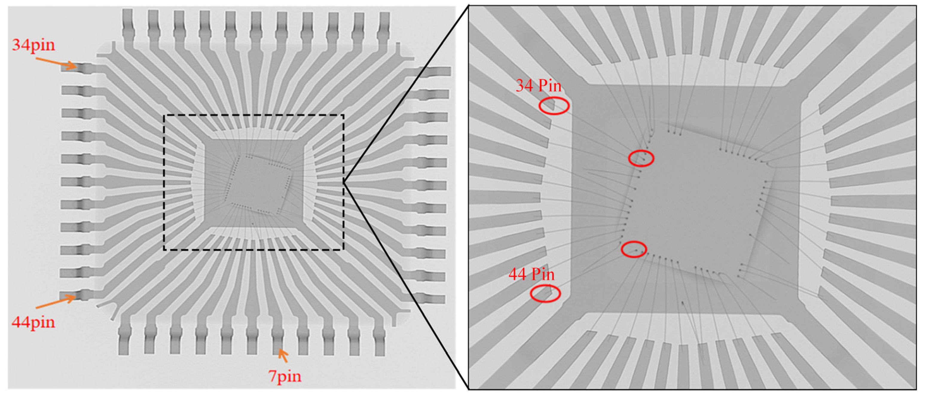
- An oscilloscope was used to monitor pins 34 and 44 of the MCU. When the MCU was working normally, pin 44 output a PWM pulse, and pin 34 produced a communication signal level at a regular time interval. The reason for choosing these two pins is because the system clock is used to coordinate and control various inputs and outputs of the system, and generally uses rising edge triggering, making it very sensitive to instantaneous electromagnetic interference. Pin 44 can serve as an output observation window. In addition, another port of the oscilloscope was used to monitor the output waveform of the EMP simulator.
- (2)
- The MCU was placed in the TEM cell while in working condition. Each time a set of data was measured, the plate was rotated 90° counterclockwise, and the measurement was repeated under the same conditions. Hence, measurements were collected at a total of four positions. Please note that when pins 1–11 were parallel with the x-axis of the TEM cell, the angle was defined as 0°.
- (3)
- During the test, different storage capacitors were used to change the FWHM of the pulse, and the breakdown voltage was adjusted by changing the pressure of the air gap switch at the power source (i.e., the amplitude of the voltage).
- (4)
- Starting from the smallest storage capacitance, the initial air pressure was 1 atm, and the electrode distance was 2 mm, which remained constant. Each group of tests was repeated three times, and then the air pressure was increased by 1 atm until the pressure reached 4 atm. Then, the test plate was rotated, and the above tests were repeated. After all tests at four positions were completed, the storage capacitor was replaced. A total of three storage capacitors were used in this study.
4. Results and Analysis
4.1. Results
- (1)
- Storage capacitance (FWHM/rising edge)–pressure (field strength)–angle tests
- (2)
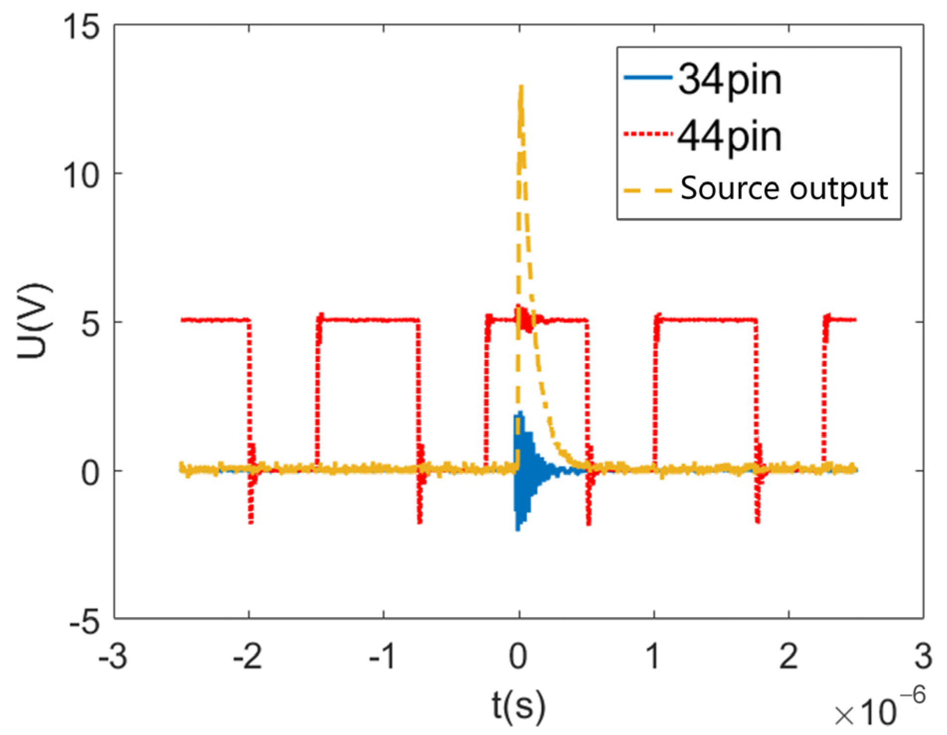
- Output waveform
4.2. Analysis
5. Conclusions
Author Contributions
Funding
Institutional Review Board Statement
Informed Consent Statement
Data Availability Statement
Conflicts of Interest
References
- Sabath, F.; Potthast, S. Tolerance values and the confidence level for high-altitude electromagnetic pulse (HEMP) field tests. IEEE Trans. Electromagn. Compat. 2013, 55, 518–525. [Google Scholar] [CrossRef]
- Fichte, L.O.; Knoth, S.; Potthast, S.; Sabath, F.; Stiemer, M. On the validity and statistical significance of HEMP test standards. In Proceedings of the 2015 IEEE International Symposium on Electromagnetic Compatibility (EMC), Dresden, Germany, 16–22 August 2015; pp. 865–870. [Google Scholar]
- Rachidi, F. A review of field-to-transmission line coupling models with special emphasis to lightning-induced voltages on overhead lines. IEEE Trans. Electromagn. Compat. 2012, 54, 898–911. [Google Scholar] [CrossRef]
- Du, Z.; Zhang, X.; Zhu, H.; Xiao, P.; Yu, X.; Xie, Y. Full-wave modeling method for high-frequency electromagnetic disturbances coupling to transmission lines. High Power Lasor Part. Beams 2023, 35, 023005-1–023005-7. [Google Scholar]
- Qi, G.; Li, K.; Li, Y.; Lv, F.; Wang, S.; Wang, Z.; Wang, D.; Xie, Y. Experimental study on effects of electromagnetic pulse on pipeline supervisory control and data acquisition (SCADA) system. High Power Laser Part. Beams 2015, 27, 123202. [Google Scholar]
- Zhou, X.; Wang, S.; Wei, G. Study on radiation effects of EMP on digital circuits. High Volt. Eng. 2006, 32, 46–49. [Google Scholar]
- Fang, J.; Shen, J.; Yang, Z.; Qiao, D. Experimental study on microwave vulnerability effect of integrated circuit. High Power Laser Part. Beams 2003, 15, 591–594. [Google Scholar]
- Paknahad, J.; Sheshyekani, K.; Rachidi, F.; Paolone, M. Lightning electromagnetic fields and their induced currents on buried cables. Part II: The effect of a horizontally stratified ground. IEEE Trans. Electromagn. Compat. 2014, 56, 1146–1154. [Google Scholar] [CrossRef]
- Tesche, F.M. On the analysis of a transmission line with nonlinear terminations using the time-dependent BLT equation. IEEE Trans. Electromagn. Compat. 2007, 49, 427–433. [Google Scholar] [CrossRef]
- IEC62132-4; Integrated Circuits-Measurement of Electromagnetic Immunity 150 khz to 1 ghz-Part 4: Direct rf Power Injection Method. Draft Technical Report. IEC: Geneva, Switzerland, 2006.
- IEC62132-1; Integrated Circuits-Measurement of Electromagnetic Immunity 150 khz to 1 ghz-Part 1: General Conditions and Definitions. Draft Technical Report. IEC: Geneva, Switzerland, 2006.
- Tesche, F.M.; Ianoz, M.; Karlsson, T. EMC Analysis Methods and Computational Models; John Wiley & Sons: Hoboken, NJ, USA, 1996. [Google Scholar]
- Chen, Y.; Xie, Y.; Lium, M.; Gao, C.; Li, M.; Gong, S.; Zhou, J. Analysis of high-altitude electromagnetic effect models on power system. High Power Laser Part. Beams 2019, 31, 070007. [Google Scholar]
- Grivet-Talocia, S.; Huang, H.M.; Ruehli, A.E.; Canavero, F.; Elfadel, I.M. Transient analysis of lossy transmission lines: An efficient approach based on the method of characteristics. IEEE Trans. Adv. Packag. 2004, 27, 45–56. [Google Scholar] [CrossRef] [Green Version]
- Erdin, I.; Dounavis, A.; Achar, R.; Nakhla, M.S. A spice model for incident field coupling to lossy multiconductor transmission lines. IEEE Trans. Electromagn. Compat. 2001, 43, 485–494. [Google Scholar] [CrossRef]
- Dounavis, A.; Achar, R.; Nakhla, M.S. Efficient passive circuit models for distributed networks with frequency-dependent parameters. IEEE Trans. Adv. Packag. 2000, 23, 382–392. [Google Scholar] [CrossRef]
- Nakhla, N.M.; Dounavis, A.; Achar, R.; Nakhla, M.S. DEPACT: Delay extraction-based passive compact transmission-line macromodeling algorithm. IEEE Trans. Adv. Packag. 2005, 28, 13–23. [Google Scholar] [CrossRef]
- Xie, Y.Z.; Canavero, F.G.; Maestri, T.; Wang, Z.J. Crosstalk analysis of multiconductor transmission lines based on distributed analytical representation and iterative technique. IEEE Trans. Electromagn. Compat. 2010, 52, 712–727. [Google Scholar] [CrossRef]
- Jin, M.; Weiming, M.; Lei, Z. Parameter estimation of lumped circuit models for conducted EMI in power converters. Trans. China Electrotech. Soc. 2005, 20, 25–29. [Google Scholar]
- Fang, X.; Li, S. Predicting conducted electromagnetic interference for IGBT switching module in power converter systems. Proc. CESS 2012, 32, 157–164. [Google Scholar]
- Yang, X.; Long, Z.; Wen, Y.; Huang, H.; Palmer, P.R. Investigation of the trade-off between switching losses and EMI generation in Gaussian S-shaping for high-power IGBT switching transients by active voltage control. IET Power Electron. 2016, 9, 1979–1984. [Google Scholar] [CrossRef]
- Oswald, N.; Stark, B.H.; Holliday, D.; Hargis, C.; Drury, B. Analysis of shaped pulse transitions in power electronic switching waveforms for reduced EMI generation. IEEE Trans. Ind. Appl. 2011, 47, 2154–2165. [Google Scholar] [CrossRef]
- Jiang, Y.; Chen, P.; Liu, W.; Zhang, K. Common-mode EMI behavior of an IGBT Buck converter. High Volt. Eng. 2008, 34, 2234–2239. [Google Scholar]
- Deren, F.; Feng, Y.; Mengfei, L. Electromagnetic interference of repetitive frequency electromagnetic pulses toward trigger system of thyristor. High Volt. Eng. 2014, 40, 2693–2698. [Google Scholar]
- Liu, X.; Wang, Y.; Li, X. Design and Implementation of ADC digital circuit based on MCU. China Integr. Circuit 2022, 31, 32–35. [Google Scholar]


| Storage Capacitor (pF) | Angle (°) | Pressure (atm) | FWHM (ns) | Voltage (kV) | Electric Field Intensity (kV/m) | Pin 34 Vp (V) | Pin 44 Vp (V) |
|---|---|---|---|---|---|---|---|
| 15,000 | 0 | 1 | 524.53 | 13.2 | 88 | 1.9 | 7.76 |
| 2 | 503.87 | 16.07 | 107.11 | 2.3 | 8.08 | ||
| 3 | 489.6 | 18.47 | 123.11 | 3.06 | 8.28 | ||
| 4 | 478.8 | 20.73 | 138.22 | 3.51 | 8.43 | ||
| 90 | 1 | 513.07 | 14.6 | 97.33 | 2.37 | 7.81 | |
| 2 | 510.67 | 15.47 | 103.11 | 2 | 7.8 | ||
| 3 | 500.53 | 17.13 | 114.22 | 2.21 | 7.88 | ||
| 4 | 483.6 | 20.4 | 136 | 3.04 | 8.24 | ||
| 180 | 1 | 545.87 | 12.67 | 84.44 | 1.7 | 7.49 | |
| 2 | 518.93 | 14.93 | 99.56 | 2.22 | 7.6 | ||
| 3 | 493.73 | 18.33 | 122.22 | 2.78 | 7.8 | ||
| 4 | 482.93 | 20.4 | 136 | 3.15 | 7.94 | ||
| 270 | 1 | 566.27 | 11.73 | 78.22 | 1.89 | 7.44 | |
| 2 | 498.67 | 18.13 | 120.89 | 3.49 | 7.69 | ||
| 3 | 493.47 | 18.4 | 122.67 | 3.53 | 7.73 | ||
| 4 | 477.73 | 20.47 | 136.44 | 4.03 | 7.99 |
| Storage Capacitor (pF) | Angle (°) | Pressure (atm) | FWHM (ns) | Voltage (kV) | Electric Field Intensity (kV/m) | Pin 34 Vp (V) | Pin 44 Vp (V) |
|---|---|---|---|---|---|---|---|
| 5793 | 0 | 1 | 236.13 | 10.8 | 72 | 1.42 | 7.29 |
| 2 | 228.4 | 13.67 | 91.11 | 1.29 | 7.31 | ||
| 3 | 213.33 | 16.87 | 112.45 | 1.96 | 7.39 | ||
| 4 | 198.27 | 21.13 | 140.89 | 3.14 | 7.87 | ||
| 90 | 1 | 230.4 | 12.33 | 82.22 | 1.37 | 7.47 | |
| 2 | 227.87 | 13.2 | 88 | 0.91 | 7.37 | ||
| 3 | 223.87 | 15 | 100 | 1.28 | 7.44 | ||
| 4 | 195.87 | 21.27 | 141.78 | 2.73 | 8.05 | ||
| 180 | 1 | 235.73 | 11.13 | 74.22 | 1.62 | 7.57 | |
| 2 | 223.6 | 14.07 | 93.78 | 1.85 | 7.76 | ||
| 3 | 215.33 | 16.8 | 112 | 1.85 | 7.76 | ||
| 4 | 201.47 | 20.13 | 134.22 | 3.06 | 8.25 | ||
| 270 | 1 | 227.07 | 11.8 | 78.67 | 2 | 7.45 | |
| 2 | 211.6 | 15.53 | 103.56 | 3.03 | 7.75 | ||
| 3 | 214.27 | 17 | 113.33 | 2.96 | 7.63 | ||
| 4 | 195.33 | 21.6 | 144 | 4.41 | 8.2 |
| Storage Capacitor (pF) | Angle (°) | Pressure (atm) | FWHM (ns) | Voltage (kV) | Electric Field Intensity (kV/m) | Pin 34 Vp (V) | Pin 44 Vp (V) |
|---|---|---|---|---|---|---|---|
| 1910 | 0 | 1 | 90.4 | 10.27 | 68.44 | 1.14 | 7.44 |
| 2 | 84.8 | 15.13 | 100.89 | 1.7 | 7.61 | ||
| 3 | 84 | 16.2 | 108 | 1.69 | 7.68 | ||
| 4 | 81.33 | 20.6 | 137.33 | 2.37 | 8.33 | ||
| 90 | 1 | 86.2 | 12.35 | 82.33 | 2.26 | 7.52 | |
| 2 | 87.73 | 14.07 | 93.78 | 1.49 | 7.51 | ||
| 3 | 82.53 | 16.73 | 111.56 | 2.02 | 7.76 | ||
| 4 | 81.07 | 19.93 | 132.89 | 2.56 | 7.93 | ||
| 180 | 1 | 87.87 | 11.87 | 79.11 | 2.04 | 7.81 | |
| 2 | 87.07 | 13.27 | 88.44 | 1.59 | 7.47 | ||
| 3 | 82.13 | 17.93 | 119.56 | 2.83 | 8.13 | ||
| 4 | 78.67 | 21.13 | 140.89 | 2.92 | 8.49 | ||
| 270 | 1 | 87.33 | 11.6 | 77.33 | 1.89 | 7.67 | |
| 2 | 84.13 | 14.33 | 95.56 | 1.96 | 8.19 | ||
| 3 | 84.93 | 16.27 | 108.45 | 1.86 | 8.24 | ||
| 4 | 79.87 | 20.07 | 133.78 | 3.25 | 8.74 |
| Position (°) | 1 atm | 2 atm | 3 atm | 4 atm | Total |
|---|---|---|---|---|---|
| 0 | 0 | 0 | 0 | 0 | 0 |
| 90 | C1, C3 | 0 | 0 | 0 | 2 |
| 180 | 0 | 0 | C3 | 0 | 1 |
| 270 | C2 | C1, C2, C3 | C1, C2 | C1, C2, C3 | 9 |
| Position (°) | 1 atm | 2 atm | 3 atm | 4 atm | Total |
|---|---|---|---|---|---|
| 0 | C3 | 0 | C3 | C3 | 3 |
| 90 | C2 | C1, C2, C3 | C1, C2 | C1, C2 | 8 |
| 180 | C1 | 0 | 0 | 0 | 1 |
| 270 | 0 | 0 | 0 | 0 | 0 |
| Position (°) | 1 atm | 2 atm | 3 atm | 4 atm | Total |
|---|---|---|---|---|---|
| 0 | 0 | C1 | C1 | C1 | 3 |
| 90 | C1 | 0 | 0 | 0 | 1 |
| 180 | C2, C3 | C2 | C2 | C2 | 5 |
| 270 | 0 | C3 | C3 | C3 | 3 |
| Position (°) | 1 atm | 2 atm | 3 atm | 4 atm | Total |
|---|---|---|---|---|---|
| 0 | C2, C3 | C2 | C2, C3 | C2 | 6 |
| 90 | 0 | 0 | 0 | C3 | 1 |
| 180 | 0 | C1, C3 | 0 | C1 | 3 |
| 270 | C1 | 0 | C1 | 0 | 2 |
| Storage Capacitance (pF) | Maximum Interference (Number of Groups) | Minimal Interference (Number of Sets) |
|---|---|---|
| 15,000 | A, B, C, D, E, F, G, H, J, L, N, O | 0 |
| 5793 | M, P | B, E, F, G, I, K |
| 1910 | I, K | A, C, D, H, J, L, M, N, O, P |
Disclaimer/Publisher’s Note: The statements, opinions and data contained in all publications are solely those of the individual author(s) and contributor(s) and not of MDPI and/or the editor(s). MDPI and/or the editor(s) disclaim responsibility for any injury to people or property resulting from any ideas, methods, instructions or products referred to in the content. |
© 2023 by the authors. Licensee MDPI, Basel, Switzerland. This article is an open access article distributed under the terms and conditions of the Creative Commons Attribution (CC BY) license (https://creativecommons.org/licenses/by/4.0/).
Share and Cite
Fan, L.; Zu, X.; Huang, Z. Interferences of Electromagnetic Pulses on Microcontroller Units. Appl. Sci. 2023, 13, 8190. https://doi.org/10.3390/app13148190
Fan L, Zu X, Huang Z. Interferences of Electromagnetic Pulses on Microcontroller Units. Applied Sciences. 2023; 13(14):8190. https://doi.org/10.3390/app13148190
Chicago/Turabian StyleFan, Linjing, Xudong Zu, and Zhengxiang Huang. 2023. "Interferences of Electromagnetic Pulses on Microcontroller Units" Applied Sciences 13, no. 14: 8190. https://doi.org/10.3390/app13148190
APA StyleFan, L., Zu, X., & Huang, Z. (2023). Interferences of Electromagnetic Pulses on Microcontroller Units. Applied Sciences, 13(14), 8190. https://doi.org/10.3390/app13148190