Review

A Short Review of Through-Silicon via (TSV) Interconnects: Metrology and Analysis

1
Department of Materials Science and Engineering, Harbin Institute of Technology (Shenzhen), Shenzhen 518055, China
2
Science and Technology on Reliability Physics and Application of Electronic Component Laboratory, China Electronic Product Reliability and Environmental Testing Research Institute, Guangzhou 510640, China
3
Sauvage Laboratory for Smart Materials, Harbin Institute of Technology (Shenzhen), Shenzhen 518055, China
*
Authors to whom correspondence should be addressed.
These authors contributed equally to this work.
Appl. Sci. 2023, 13(14), 8301; https://doi.org/10.3390/app13148301
Submission received: 22 May 2023 / Revised: 4 July 2023 / Accepted: 15 July 2023 / Published: 18 July 2023

Abstract

:
This review investigates the measurement methods employed to assess the geometry and electrical properties of through-silicon vias (TSVs) and examines the reliability issues associated with TSVs in 3D integrated circuits (ICs). Presently, measurements of TSVs primarily focus on their geometry, filling defects, and the integrity of the insulating dielectric liner. Non-destructive measurement techniques for TSV contours and copper fillings have emerged as a significant area of research. This review discusses the non-destructive measurement of contours using high-frequency signal analysis methods, which aid in determining the stress distribution and reliability risks of TSVs. Additionally, a non-destructive thermal detection method is presented for identifying copper fillings in TSVs. This method exploits the distinct external characteristics exhibited by intact and defective TSVs under thermoelectric coupling excitation. The reliability risks associated with TSVs in service primarily arise from copper contamination, thermal fields in 3D-ICs, stress fields, noise coupling between TSVs, and the interactions among multiple physical fields. These reliability risks impose stringent requirements on the design of 3D-ICs featuring TSVs. It is necessary to electrically characterize the influence of copper contamination resulting from the TSV filling process on the reliability of 3D-ICs over time. Furthermore, the assessment of stress distribution in TSVs necessitates a combination of micro-Raman spectroscopy and finite element simulations. To mitigate cross-coupling effects between TSVs, the insertion of a shield between them is proposed. For efficient optimization of shield placement at the chip level, the geometric model of TSV cross-coupling requires continuous refinement for finite element calculations. Numerical simulations based on finite element methods, artificial intelligence, and machine learning have been applied in this field. Nonetheless, comprehensive design tools and methods in this domain are still lacking. Moreover, the increasing integration of 3D-ICs poses challenges to the manufacturing process of TSVs.

1. Introduction

The advancement of 3D IC technology presents a promising solution for the continuation of “more Moore’s law” in the future. However, a major challenge in the development of 3D IC technology is the establishment of reliable and high-performance 3D circuits and systems. The implementation of 3D technology helps alleviate problems associated with interconnection delays by reducing gate delays and increasing interconnections through the use of shorter wires. These shorter wires help reduce the average load capacitance and resistance, resulting in a decrease in the number of repeaters required to regenerate the signal on long wires [1,2]. Vertical stacking of ICs has become a viable option in the semiconductor industry for reducing wirelength and integration. For example, stacking DRAM on top of processor cores helps to increase CPU-DRAM bandwidth, while stacking processor cores vertically can increase inter-core communication bandwidth. To enable vertical stacking, vertical interconnects are required, with the most common type being the silicon through-hole [3,4,5].
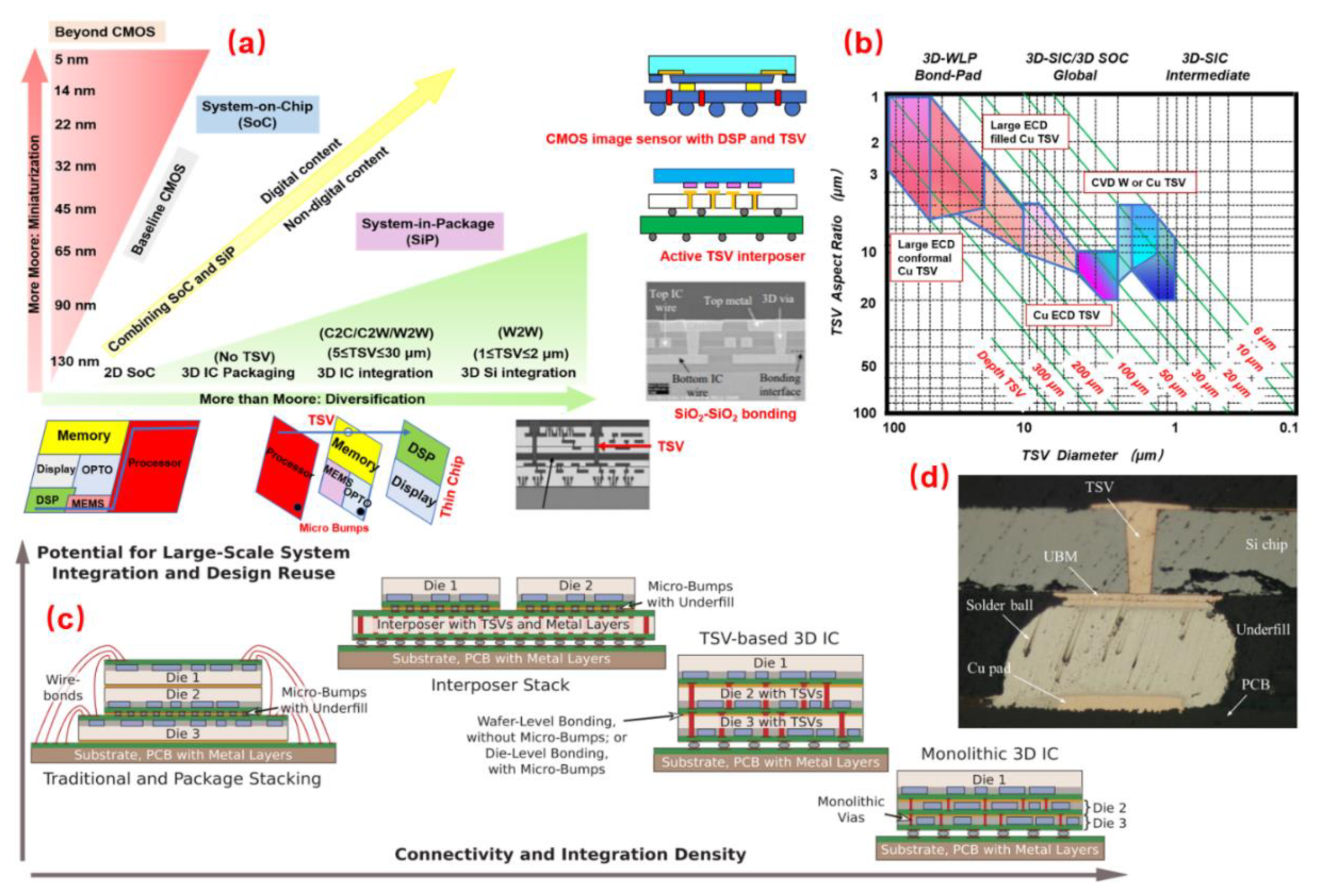
Three-dimensional integration refers to a configuration and technique used to vertically integrate multiple chips by means of wafer bonding and electrical interconnections using through-silicon vias (TSVs, Figure 1). The idea of utilizing hollow vias for signal transmission through a wafer was first proposed by Shockley in 1958. Subsequently, in 1964, IBM explicitly introduced the concept of etching and metal deposition for TSV fabrication. In 1969, IBM further proposed a 3D integration method employing double-sided KOH etching and metal deposition to create TSVs, with metal solder employed for chip bonding. However, it was not until 1984 that the stacking of CMOS chips in a three-dimensional configuration was achieved. The introduction of Bosch deep reactive ion etching (DRIE) technology in the mid-1990s made it possible to etch vertical and deep through-holes in silicon wafers, enabling the fabrication of TSVs with high aspect ratios filled with tungsten (W) or polysilicon conductors by the end of the last century. Since the year 2000, copper (Cu) plating in deep via holes has emerged as the primary technology for filling high aspect ratio TSVs [6,7,8]. The goal of electroplating is low stress, free of holes and voids during TSV fabrication [9]. TSV technology enables high-density interconnection in the z-axis direction, which significantly reduces the three-dimensional size of the microsystem. The shortened interconnect length also results in lower chip power consumption, improves data propagation speed, reduces signal delay, and improves the electrical interconnection reliability of the system. As a result, TSV technology is crucial to the success of 3D IC technology, and it has the potential to revolutionize the semiconductor industry.
Figure 1. (a) Progression of packaging technology; (b) roadmap for TSV diameter and aspect ratio; (c) 3D chips; (d) TSV package samples (adapted from [6,10,11,12]).
Applsci 13 08301 g001
As technology advances and systems are designed to improve their performance, the physical size of the channels continues to decrease. In the case of through-silicon via (TSV) technology, the diameter of the via has reduced to less than 10 μm, while the pitches have reduced to tens of microns. This miniaturization of TSVs has resulted in the increase in I/Os to tens of thousands of orders of magnitude for wide bandwidth data transmission. However, such small structures are highly susceptible to defects, which can negatively impact the performance of the integrated circuit. To achieve a highly accurate manufacturing process for these small structures, it is essential to understand the root causes of defects in TSVs. A common type of TSV defect is a void, which can occur during the deposition of the copper layer or the chemical mechanical planarization (CMP) process. The formation of a void in the TSV can result in increased electrical resistance, decreased mechanical strength, and even device failure. Other types of defects, such as misalignment, non-uniform deposition, and incomplete filling, can also occur during the fabrication process and cause TSV failure. In addition, there are the following defects: (i) The thermal expansion coefficients of copper, silicon oxide, and silicon filler materials in TSV differ greatly, triggering a thermal mismatch that can lead to plastic deformation of the copper pillar and, thus, generate cracks, damaging the surrounding cover layer and metal connection layer [10,13,14]; (ii) along with the shortening of the interconnect line length and the increase in signal transmission rate comes a significant increase in power density, which will lead to a sharp increase in temperature, thus, inducing stress concentration, electromigration, negative bias instability, and the diffusion of copper atoms [15,16,17]; (iii) TSV interconnect lines have delay, loss, and crosstalk problems, and electromigration effects tend to trigger Kirkendall holes to form cracks [18,19]; (iv) since TSVs are affected by a variety of factors under the joint action of thermal–electrical–force fields in service, an analysis method that can be simulated, modeled, and monitored in real time is needed [20,21].
Due to the significant increase in power density per unit area, the issue of thermal reliability in 3D integrated systems has become more prominent. At the same time, thermal stresses are introduced into 3D integrated systems due to a mismatch in the coefficient of thermal expansion (CTE) between materials during TSV fabrication, which affects the carrier mobility of the electronic device. When voltage is applied to the integrated system, Joule heat is generated. Joule heating increases temperature, which affects electrical parameters and thermal conductivity. The reliability of TSVs is a multi-physical field coupling problem that requires simultaneous consideration of thermal, electrical, and mechanical reliability [9].
To mitigate these defects, various strategies have been proposed, including improving the TSV manufacturing process, such as optimizing the deposition parameters and improving the CMP process. The use of advanced metrology techniques, such as X-ray microtomography and focused ion beam (FIB) milling, has also been proposed to detect and characterize defects in TSVs. In addition, post-fabrication testing and analysis methods, such as electrical and thermal analysis, can be used to identify and evaluate the impact of TSV defects on the performance of the integrated circuit.
Overall, as TSV technology continues to miniaturize, the manufacturing process must be optimized to reduce defects and improve the reliability and performance of integrated circuits. The development of effective defect detection and characterization techniques will play a crucial role in achieving this goal [21] (Figure 1). As TSV processes reach today’s level of maturity, reliability investigations become critical. This review will summarize the progress made by industry and academia on this issue in recent years.

2. TSV Metrology

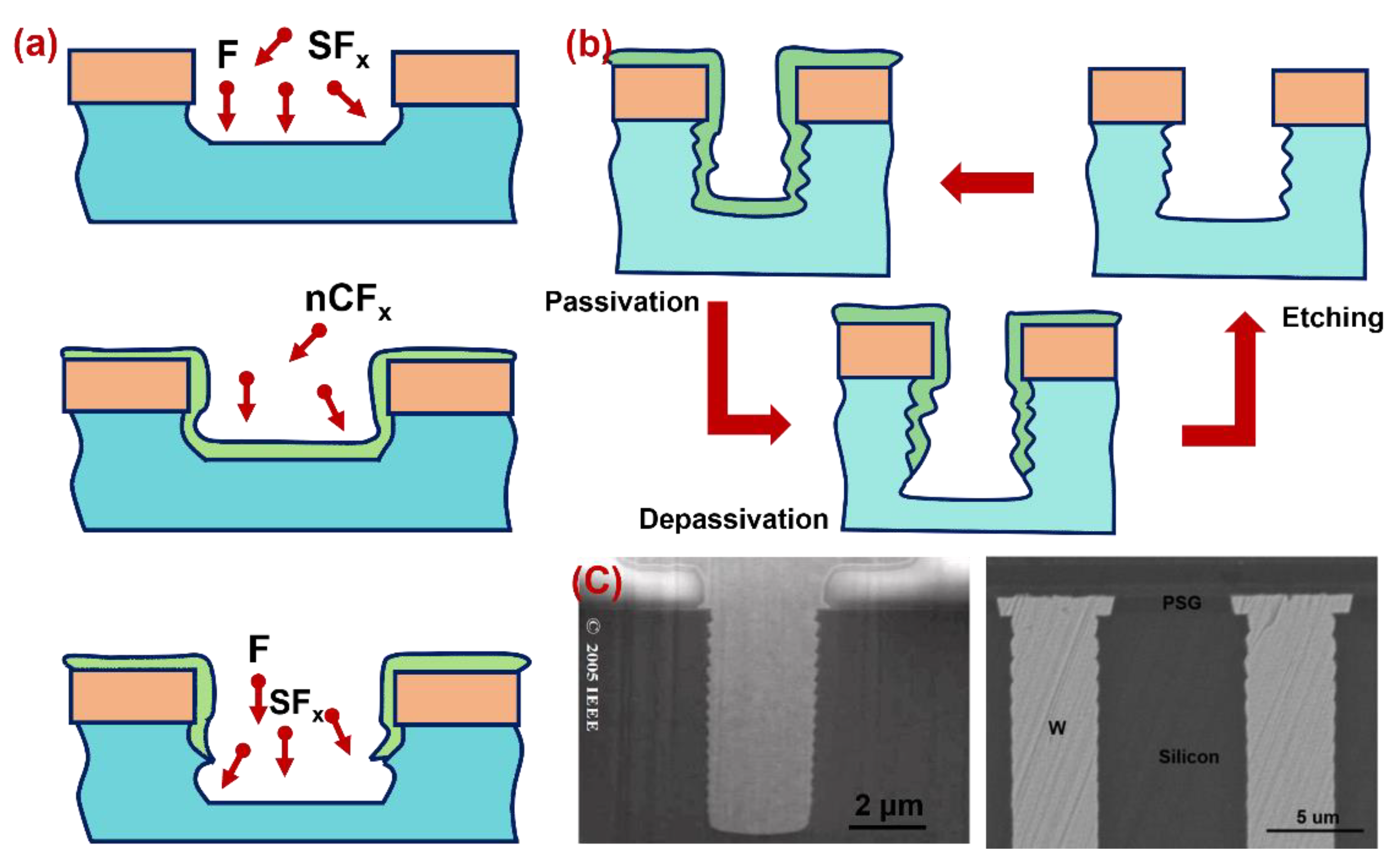
Etching is the basis of the whole TSV preparation process, which directly affects the subsequent seed layer deposition effect and has a great impact on the TSV filling quality and service reliability. TSV etching has many requirements, including good control of through-hole dimensions (through-hole depth and width), sufficient selectivity for etch masks, minimal sidewall roughness, and high throughput. The TSV etch is typically performed using reactive ion etching (RIE) to create high aspect ratio vias. The current mainstream method of etching is deep reactive ion etching (DRIE), invented by Bosch (Robert Bosch GmbH), which uses SF6 as the reactive gas to etch silicon while periodically releasing C4F8 as a passivation gas to protect the sidewalls to achieve high aspect ratio vertical TSV etching [22] (Figure 2). The process alternates between deposition and etch steps to fabricate deep vias [10]. Except for in specific environments, the Bosch process is widely used, which allows deep features to be etched in Si at etch rates ranging from 1 to 3 μm/min with a 50:1 to 100:1 mask material selectivity for photoresists and a 150:1 to 200:1 selectivity for photoresists for oxide masks [22,23,24].
DRIE or deep reactive ion etching is a popular technique for etching deep and precise holes in silicon wafers. While DRIE offers excellent controllability in terms of creating intricate patterns and structures, there are still some reliability concerns that need to be addressed. One such issue is the occurrence of sidewall defects that can affect the overall quality and integrity of the structure. To ensure the quality of the structures produced by DRIE, TSV inspection is carried out. TSV inspection can be divided into two categories of parameters. The first category is post-RIE inspection, which is performed to measure critical dimensions, depth, and profile, including the sidewall angle and through-hole curvature. This helps ensure that the structures meet the required specifications and tolerances. The second category of TSV inspection is metal fill, which is carried out to check for voids that may be present in the metal layer used to fill the holes. Voids can cause reliability problems, such as electrical shorts or open circuits, so it is essential to identify and eliminate them. By performing both types of TSV inspection, manufacturers can ensure that the structures produced by DRIE are of high quality and reliability [10].
Because of the finite electron and hole mobility in silicon and because the via MOS junction capacitance will introduce additional distributed parameters, namely, inductance, dissipation, and skin depth, it is very difficult to succinctly describe equivalent electrical parameters. TSVs are essentially metal insulator semiconductor (MIS) devices with a dielectric layer of SiO2 deposited to isolate the metal from the substrate. Due to the extremely wide bandwidth and high frequency, the corresponding TSV modeling and design will be very different from its conventional frequency band counterparts. When TSVs operate in the low frequency range, the metal oxide semiconductor (MOS) effect in TSVs should be carefully considered and modeled as MOS capacitance. When the TSV operates in the UHF and very high frequency (millimeter wave range) range, the effect of MOS capacitance on the TSV electrical performance decreases and some key issues that have a significant impact on the TSV performance need to be considered. One of the important issues is the sidewall roughness, which can generate large leakage currents in the high frequency range and severely affect the current flowing through the TSV. The effect of roughness needs to be considered in the millimeter wave frequency range due to the skinning effect [25,26].
Figure 2. (a) Etching schematic; (b) Bosch process schematic (c); TSV samples (adapted from [22]).
Applsci 13 08301 g002

2.1. Profile

In the world of 3D semiconductor packaging, TSVs or through-silicon vias play a crucial role in enabling the electrical connection of vertically stacked wafers. As a result, it is essential to monitor and control the profile of the TSVs to ensure that they are defect-free, as any issues in these holes can lead to electrical disconnections between stacked wafers.
In recent years, TSV technology has made significant progress, allowing for the creation of holes smaller than 10 μm and length-to-diameter ratios greater than 10. However, accurately measuring the profile of these TSV holes using traditional optical metrology methods has become increasingly difficult. To overcome this challenge, destructive methods, such as scanning electron microscopy (SEM) and tunneling electron microscopy (TEM), are commonly used to measure the profile of TSV holes for process development and quality control. However, these methods cannot be used for non-destructive TSV metrology, as they are time-consuming and the samples are destroyed in the process.
Therefore, there is a need for new measurement methods that can provide non-destructive and in-line TSV metrology to enable the development of better TSV processes. Researchers are exploring various techniques, such as X-ray computed tomography (XCT), infrared microscopy, and terahertz spectroscopy [27], which could potentially offer a faster, non-destructive, and more accurate way of measuring TSV profiles. Non-destructive fault isolation (FI) techniques play a crucial role in detecting multiple faults within complex 3D packages, leading to reduced production time and improved success rates. In the case of open circuit and high resistance faults, time domain reflectometry (TDR) and electro-optical terahertz pulse reflectometry (EOTPR) have demonstrated effectiveness in system-in-package (SIP) configurations with package-on-package (POP) arrangements. TDR, a cost-effective and conventional non-destructive FI technique, is employed for identifying electrical faults in flip chip packages. It involves injecting step electrical pulses with a rise time of 35–40 ps into the package interconnect and analyzing the changes in impedance along the circuit by interpreting the reflected signals acquired from the package. By comparing the reflected waves from the faulty cell with those from a known reference cell and the bare substrate, the location of the fault can be pinpointed within the chip or package substrate. The resolution of TDR depends on the rise time, bandwidth of the TDR system, and material properties present within the package. The time domain resolution of TDR can be estimated as approximately 1/10th to 1/5th of the TDR rise time.
The key to pinpointing short-circuit faults in 3D microelectronic packages is to obtain z-dimensional information about the defect in addition to x and y position data. Locked-in thermography (LIT) is a very promising technique designed to locate hot spots caused by short-term faults using a real-time graphical locking method designed to detect small signals hidden in higher intensity random noise. Scanning superconducting quantum interference device (SQUID) microscopy (SSM) has been applied as a non-destructive FI technique for short failures in conventional packages [27].
By developing more precise and reliable TSV metrology methods, manufacturers can enhance the quality and performance of 3D semiconductor packaging, paving the way for further advancements in the field. The geometrical shape of the TSV hole is defined by the following three parameters: top CD (diameter of the TSV hole on the surface, which can be measured using visible light), bottom CD (diameter of the TSV hole at the bottom, which is difficult to be measured using the visible light directly), and the depth of the TSV hole. Pan et al. [28] pointed out that the diameter, aspect ratio, and defects of the TSV hole all have an effect on the thermal behavior and stress field of the TSV structure. The total equivalent stress and deformation increase significantly with increasing TSV diameter. The aspect ratio has no effect on the total equivalent stress, but has a significant effect on the total deformation, especially for larger diameters. In addition, the larger the diameter, the more pronounced the effect. The equivalent stresses and deformations (from the center of the TSV to the edge of Si layer) increase with increasing diameter. The maximum stress is located at the Cu/SiO interface, and the maximum deformation is concentrated at the edge of Si layer.
Peng et al. [29] have proposed an innovative optical method for non-invasive detection of TSV geometry, called the high-frequency signal analysis (HFSA) method. This method involves irradiating the TSV hole with a laser beam and collecting the scattered light in the pupil plane. The scattered light carries information about the hole, and the high-frequency spectral signal in the pupil plane can be analyzed to derive the 3D profile of the hole. However, as this technique heavily relies on the diffracted high-frequency spectral signal obtained from the pupil data, accurate physical modeling methods are required to simulate the interaction between the incident point and the TSV hole. To accomplish this, the researchers used finite-difference time-domain (FDTD) analysis as a rigorous solver to calculate the pupil data for TSV diffraction.
The HFSA method has several advantages, including being a non-destructive and in-line method of measuring TSV geometry. Moreover, it offers high sensitivity and resolution, making it ideal for measuring small TSVs with high aspect ratios. Additionally, the method is fast, allowing for real-time monitoring and feedback during TSV fabrication processes. Although the HFSA method is promising, it also has some limitations. For instance, the accuracy of the method depends on the accuracy of the physical modeling used to simulate the interaction between the laser beam and the TSV hole. Additionally, the method may not work well in the presence of surface roughness or defects. Further research is necessary to improve the accuracy and applicability of this method for TSV metrology. Overall, the HFSA method offers a potentially valuable tool for the non-invasive and accurate measurement of TSV geometry, enabling the development of more reliable and high-performance 3D semiconductor packaging processes (Figure 3).
Figure 3. FDTD schematic (adapted from [29]).
Applsci 13 08301 g003

2.2. Metal Fill

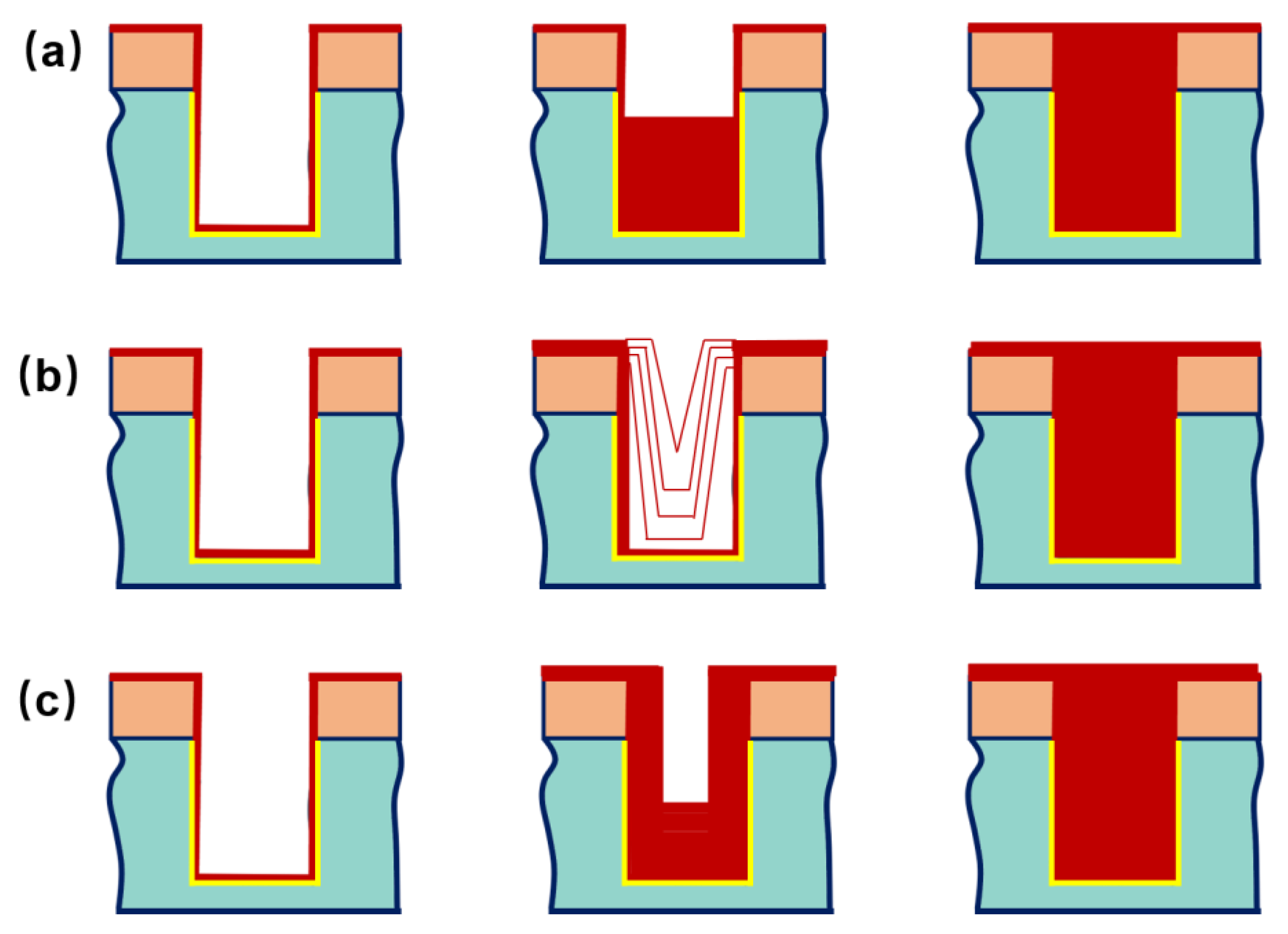
Silicon through-hole filling technology is a crucial technology for 3D integration and accounts for up to 40% of the overall cost of TSV preparation. The effectiveness of silicon via filling directly affects the reliability and yield of the device. The electrical interconnect material for most current integration processes is copper, and the mainstream process is plating. There are several plating methods for copper filling, including conformal plating, super-conformal plating, and bottom-up plating. Conformal plating is a method that uniformly deposits copper inside and on the surface of TSV holes. In contrast, bottom-up filling selectively deposits copper on the bottom of TSV holes, leaving the hole walls and surface almost unplated. Super-conformal filling combines both methods (see Figure 4). In addition to these plating methods, accelerators (SPS), inhibitors (PEG), leveling agents (JGB), etc., can be used to achieve seamless filling of TSV. These additives alter the deposition rate of copper at various locations along the hole depth direction, ensuring hole-free filling of TSV. However, the use of these additives increases the complexity of the process.
Despite these various methods for copper filling, challenges still exist. For instance, the properties of copper plating may be affected by the presence of impurities, which can lead to poor filling performance. Additionally, the large aspect ratio of TSVs makes it difficult to achieve uniform filling, which can lead to voids and other defects that affect the reliability of the device. Furthermore, the deposition of copper can lead to stress and strain in the surrounding silicon, potentially causing cracking and other issues.
Many non-destructive methods for void detection in TSV have been investigated by different researchers. X-ray computed tomography has been shown to be an effective nondestructive tool for detecting micro-voids within TSV. The use of high-frequency scanning acoustic microscopy (SAM) for TSV void detection was reported by [30]. In addition to the gigahertz-SAM technique, other acoustic-based techniques, such as laser-based acoustic analysis, are being investigated, in which signals obtained from isolated through-holes and dense arrays are compared with those from void-free TSVs. Locked-in-phase thermography (LIT) is another non-destructive technique that uses a lock-in amplifier to detect very small thermal changes in the sample. Thermal images can be studied to detect faults, such as voids in TSVs.
Figure 4. Three filling mechanisms of TSV. (a) Bottom-up plating; (b) super-conformal plating; (c) conformal Plating.
Applsci 13 08301 g004
Physical defects (Figure 5) caused by immature filling techniques, such as resistive open circuits and TSV leakage, often undermine the reliability of 3D-ICs. Furthermore, TSVs are vulnerable in the manufacturing process, and many physical defects, such as micro-voids and pin-holes, frequently occur [31,32]. Table 1 signifies the percentage difference in peak noise of defective TSVs while compared with defect free case, wherein the percentage differences in the peak noise of the partially cracked and spherical air void defected TSVs (with rcon and rhole as 2.1 nm) compared to defect-free condition are 24.23% and 1.15%, respectively, at an hTSV of 30 nm [33]. Noah et al. proposed a method that uses probes to test TSVs simultaneously, by measuring their capacitance and resistance. However, modern cantilevered probes with pitches up to 35 μm face limitations in the placement of test probes and TSVs with pitches of 4.4 μm or less. To overcome this, Chen et al. [34] suggested a solution that converts the RC parameter of TSV to voltage using charge sharing, and measures it using a sensitive amplifier.
Table 1. Percentage difference in crosstalk delay of a defective TSV compared to a defect-free case [33].
hTSV (nm)%Change in Vrosstalk Delay of Defected Conditions w.r.t Defect Free Condition
Air Crack with ConnectorSpherical AIR Void
Rcon = 1.05
nm
Rcon = 2.10
nm
Rcon = 4.20
nm
Rcon = 5.04
nm
Rhole = 1.05
nm
Rhole = 2.10
nm
Rhole = 4.20
nm
Rhole = 5.04
nm
30−1.3−0.2−0.14−0.121.00.6−1.6−3.9
60−1.7−1.3−0.37−0.161.10.7−1.3−2.9
90−1.6−0.7−0.28−0.091.20.8−0.9−1.7
120−1.5−0.5−0.16−0.031.30.9−0.2−0.6
Yi et al. [31] proposed a non-invasive solution for pre-bonded TSV testing using pulse shrinkage. This method exploits the fact that defects in the TSV cause propagation delay variations. The rise and fall times are converted into pulse widths, which are digitized using the pulse shrinkage technique to obtain a digital code. This code is then compared with the expected value of a fault-free TSV to detect any faults.
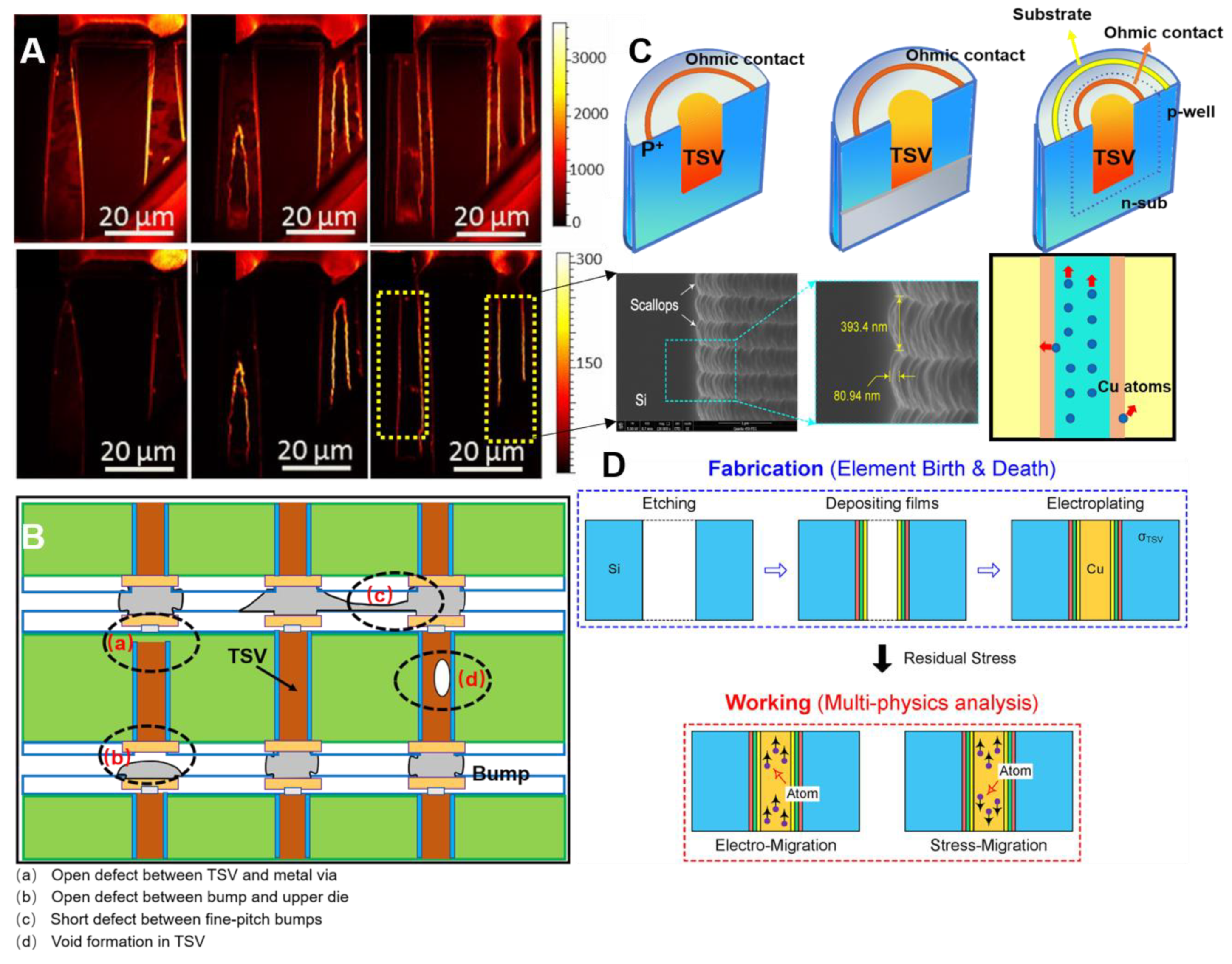
Figure 5. Physical defects of TSVs, (A) Barnes et al., used a focused ion beam (FIB) to cut the TSV to analyze Cu atom migration (adapted from [16]). Secondary ion images during the FIB slicing of a TSV with a 50 nm TiN barrier. (B) Physical defects of TSVs (adapted from [21]). (C) Relying on TSV for electrical interconnection. (D) Numerical simulation flow: residual stress analysis based on element birth and death technique and migration analysis based on multi-physics analysis. (adapted from [35]).
Applsci 13 08301 g005
Barnes et al. [16] have used a focused ion beam (FIB) cutting technique to analyze Cu atom migration in TSVs. They acquired TOF-SIMS (time-of-flight secondary ion mass spectrometry) images to observe voids in the TSV and identify defects in the barrier layer. To achieve depth profiling of the TSV, a precise wafer dicing method was performed, followed by non-in situ plasma FIB cutting, so that only a thin SiO2 layer covered the sidewalls of the TSV. Dual-beam depth profiling was then used to examine the cut and FIB-polished side of the sample. The effectiveness of the barrier layer in Cu-TSV samples was evaluated, and a comparison between TSVs without potential barriers and those with a 50 nm thick TiN barrier was performed. This method not only characterizes the degree of TSV filling, but also enables the observation of any inhomogeneities in the thickness of the Cu and potential barriers that make up the TSV. Additionally, modern TOF-SIMS instruments equipped with FIB and other sputtering sources (Cs, O, etc.) provide versatility and allow for the analysis of the same sample using several different methods to obtain more comprehensive information. This approach can aid in the identification of TSV defects and help to optimize the manufacturing process to achieve more reliable and efficient 3D integrated circuits (Figure 5).
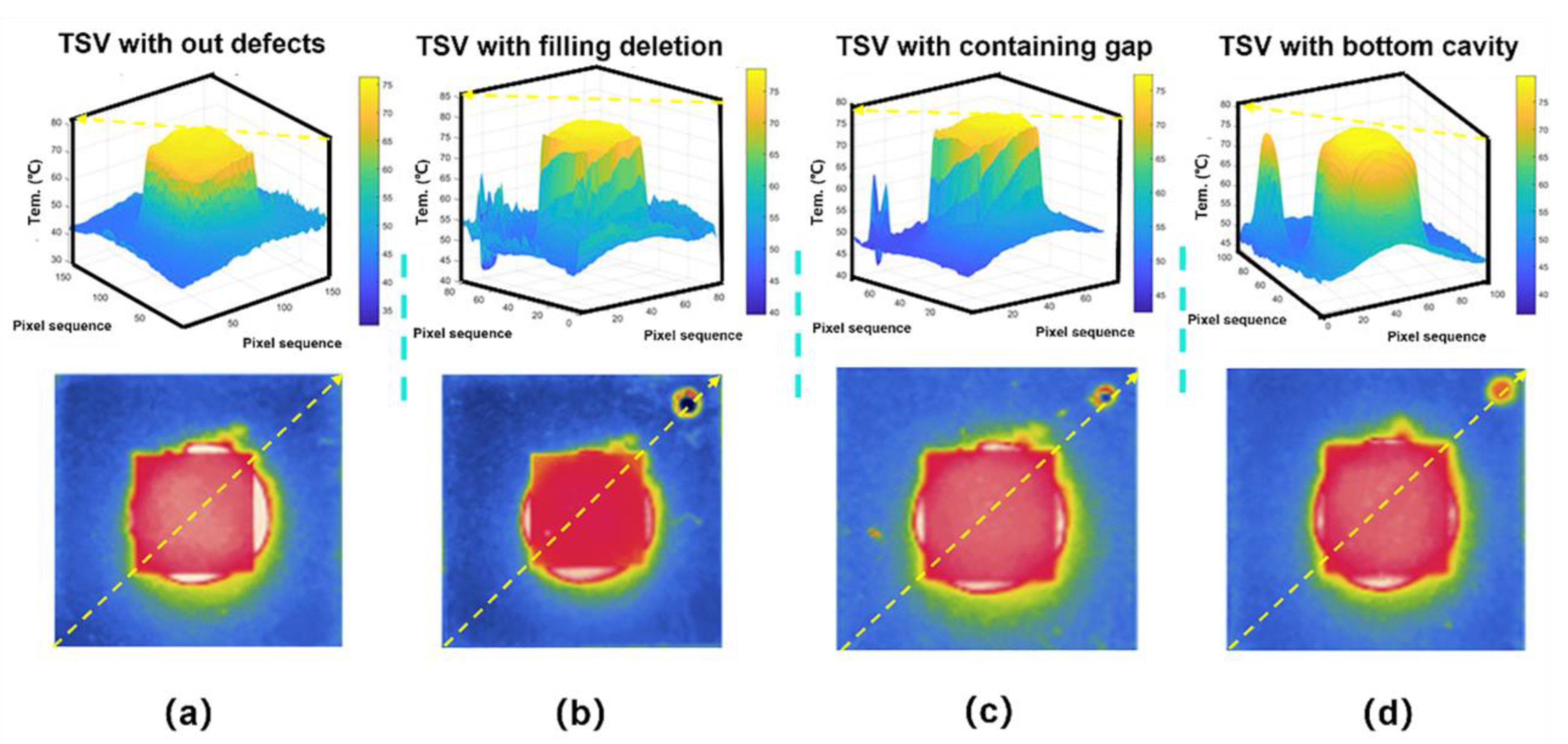
Nie et al. [36] concluded that there is a significant difference in the temperature distribution between intact TSV and defective TSV with some typical defects. The good agreement between experimental validation and simulation results shows that the method is feasible for TSV internal defect detection applications (Figure 6). The intact TSV and the defective TSV exhibit different external characteristics under thermoelectric coupling excitation. In the experiment, the test sample is placed on a heating rod. After a period, the temperature is conducted to the 3D packed sample of the TSV. At the same time, the temperature information is captured by the thermal imaging camera. The temperature of the intact TSV starts to gradually increase, and then, in the center of the TSV sample, the temperature gradually stabilizes and gradually decreases. The overall result shows a certain symmetry (Figure 6a). For TSVs with filling deletion, the heat can only be conducted along the inner wall caused by the complete absence of copper, with the lowest temperature in the center where it is missing and the highest temperature around the inner wall (Figure 6b). For TSVs containing gaps, since the TSV copper pillars contain gaps, when heat is conducted to the defect, heat will continue to transfer along the inner wall of the gap, so heat will accumulate in the gap ring and the temperature will increase (Figure 6c). For TSVs with defects in the bottom cavity, the temperature starts to rise at the defects, then tends to be smooth, and finally drops slowly. Since there are holes in the bottom, there are some barriers to heat conduction. Heat is first conducted along the copper column of the TSV without holes (Figure 6d). Therefore, the presence of defects can be clearly identified by comparing the three defects with the complete TSV.
In addition to this, Shang and Sun [36] proposed a multi-tone tuning jitter test method. First, the TSV defect equivalent circuit is obtained, and the multi-tone signal with Gaussian white noise is added as the excitation of the test simulation to extract the peak-to-average ratio for fault detection; the accuracy of this method can reach the micrometer level. Nair et al. [37] used Adam’s deep neural network algorithm to detect faulty TSVs in 3D-IC. Compared with the traditional random gradient algorithm, it has fast performance and a better convergence speed. The simulation results are outstanding in terms of area, line length, delay, running time, and temperature.
Figure 6. Thermal images and 3D temperature distribution diagram. (a) Intact, (b) filling deletion, (c) containing gap, and (d) bottom cavity (adapted from [36]).
Applsci 13 08301 g006

2.3. Electric-Field (E-Field) and Keep-Out Zone (KOZ)

The increase in the number of silicon vias (TSVs) per unit area results in electrical channels in adjacent semiconductor devices being closer to the depletion zone induced by the electric field (E-field) surrounding the TSVs. Given these negative effects, a keep-out zone (KOZ) is required to ensure proper operation of three-dimensional integrated circuits (3-D ICs) using TSVs. All logic cells must be placed where the carriers within the PMOS/NMOS channel are not affected by the electric field (E-field) around the TSV [38]. There are several ways to determine the no-go zone (KOZ) of 3-D ICs. Kabiem’s research show that for an accurate KOZ, the charge carriers in the depletion zone and the charge type defects in the TSV must be considered [39] (Figure 7). In this work they developed a KOZ determination method for TSV by solving Poisson’s equation (Equation (1)). It is worth noting that, especially for transistors, stress changes the carrier mobility and, thus, the performance of the transistor. As such, the size of the KOZ also depends on the size of the TSV [40]. Equations (1)–(3) are as follows:
W koz ( φ s 0 ) = r 1 exp 1 + φ s + r 1 2 τ s ( φ s ) φ s 2 + 2 r 1 2 η s ( φ s ) 1 1
τ s ( φ s ) = q N a ε S i exp q φ s K T 1 + n i 2 N a 2
W koz φ s = 0 = r 1 exp 1 + 1 + r 1 2 q N a ε s i q K T 1 1
where N a is the doping concentration in p-type Si, ε s i is the permittivity of Si, φ s is the surface electrical potential, n i is the intrinsic carrier concentration of Si, q is the electron charge, K is the Boltzmann constant, and T is the absolute temperature.
Figure 7. Charge-type imperfections, which include mobile oxide charges (Qm), oxide trap charges (Qot), fixed oxide charges (Qf), and interface trap charges (Qit) in a TSV (adapted from [39]).
Applsci 13 08301 g007
Therefore, an insulating dielectric liner needs to be deposited after the silicon via etch is complete to increase breakdown voltage and reduce leakage current. In high aspect ratio TSVs, liner, barrier, and seed deposition technologies are critical for process integration and reliability. The reliability of the liner is studied by applying a negative voltage to the TSV (known as the copper closed mode). In this stress mode, the copper ions of TSV are attracted by the voltage source and are not injected into the pad during the test. This makes it possible to study the inherent liner characteristics. The barrier performance is studied by comparing the measurement results in the copper closed mode with the measurement results obtained when a positive voltage is applied to the TSV (later known as the copper drive mode). In the latter stress mode, copper ions are pushed into the liner in the case of barrier defects. The large difference in TDDB data between the two modes may indicate poor barrier characteristics (Figure 8) [20,41].
Figure 8. Cu-confined and Cu-driven schematic (adapted from [41]). (a) TDDB data of Cu-confined model (b) TDDB data of Cu-driven model.
Applsci 13 08301 g008

3. TSV Reliability

3.1. Copper Contamination

After completing the silicon via etch in high aspect ratio TSVs, it is necessary to deposit an insulating dielectric liner to increase the breakdown voltage and reduce current leakage. The electromigration (EM) wear mechanism observed in contemporary CMOS damascene copper interconnects primarily involves void formation and expansion. Notably, the maximum divergence of current flow takes place in proximity to the via at the cathode of the line, resulting in void nucleation at the interface between copper and the dielectric layer (Cu/SiN or Cu/SiCN). This interface is particularly vulnerable due to its poor adhesion properties, leading to a high diffusion rate and making it the weakest point. Consequently, the presence of an inadequate barrier can lead to the occurrence of leakage currents. Therefore, ensuring the deposition of suitable liner, barrier, and seed technologies is essential for achieving reliable process integration [42]. In order to ensure the reliability of the liner, a negative voltage is applied to the TSV to attract copper ions towards the voltage source, preventing them from being injected into the pad during the test. This method allows for the study of the inherent characteristics of the liner. The barrier performance, on the other hand, is analyzed by comparing measurement results obtained in the copper closed mode with those obtained when a positive voltage is applied to the TSV. In case of barrier defects, copper ions are pushed into the liner during the latter stress mode. A significant difference in TDDB data between the two modes may indicate poor barrier characteristics. Therefore, it is essential to conduct these tests to ensure that the TSVs meet the desired reliability standards, and to improve the liner and barrier deposition technologies to achieve optimal performance [21,35,43].
In addition, the electrical characteristics of through-silicon vias (TSVs) are influenced by several factors, including the geometry, material properties, and temperature of the TSV. As a result, numerical calculations in simulation software become more complicated and time-consuming. To accurately model the behavior of TSVs, simulation software must consider a wide range of parameters, such as the length, width, aspect ratio, and shape of the TSV. Additionally, the electrical properties of the surrounding dielectric and conductive materials, as well as the temperature-dependent behavior of the TSV, must also be considered.
Despite the complexity of simulating TSVs, various software tools, such as the high-frequency structure simulator (HFSS) and computer simulation technology (CST), are available to calculate the transmission characteristics of TSVs. These tools employ numerical methods, such as finite element analysis (FEA) and finite difference time domain (FDTD), to model the behavior of TSVs and predict their electrical performance. By simulating TSVs using these software tools, designers can optimize the TSV geometry and material properties to achieve desired electrical characteristics, including high bandwidth, low insertion loss, and low crosstalk. The electrical characteristics of TSVs are determined by several factors, making numerical simulations complex and time-consuming. However, software tools, such as HFSS and CST, can be used to model the behavior of TSVs and predict their electrical performance. By optimizing the TSV geometry and material properties using these tools, designers can achieve the desired electrical characteristics of TSVs for high-performance electronic applications.
Atomic migration (AM) is a significant concern for the reliability of backend of line (BEOL) interconnects, which refers to the mass transport of metal atoms caused by the electron wind and intensified by temperature. Therefore, atomic migration consists of electromigration (EM), stress migration (SM), and thermal migration (TM). This phenomenon can lead to the formation of voids, which can eventually result in open circuits, causing a malfunction or failure of the interconnect. The void formation is mainly caused by the accumulation of metal atoms, which is driven by the electron wind and the thermal energy generated by the current flow. The resulting voids may initiate or propagate cracks in the surrounding dielectric layers, compromising the electrical conductivity of the interconnect. Therefore, it is essential to understand and mitigate the effects of atomic migration to enhance the reliability of BEOL interconnects. Notably, atomic migration can also be a significant reliability issue for through-silicon vias (TSVs), where the mass transport of metal atoms can cause voids, leading to the failure of the interconnect [44].
The behavior of electrons and the copper lattice in backend of line (BEOL) interconnects can lead to atomic migration, which has significant impacts on the reliability of the interconnects. Specifically, the momentum exchange between electrons and copper atoms causes the migration of copper atoms, leading to void formation in their original positions. Furthermore, copper atoms can accumulate in the silicon layer, causing contamination and the formation of mound-like protrusions. This phenomenon can be driven by a variety of physical mechanisms, including electric currents, stress gradients, and temperature gradients. Atomic migration can be classified into three types: electromigration (EM), stress migration (SM), and thermal migration (TM), which are governed by the mass balance equation.
Research by Cheng et al. [35] has shown that stress migration occurs earlier than electromigration in copper through-silicon vias (TSVs), regardless of the presence of Bosch scallops. This finding suggests that stress is a key factor in the early migration failure of copper TSVs. Moreover, significant atomic migration can be observed at both ends of the TSV and in the region around the Bosch scallop. Concentration fluctuations with a maximum amplitude of 0.38 can also be induced along the Bosch scallop interface, which increase with the width of the Bosch scallop. However, reducing the Bosch scallop width to below 20 nm can avoid significant atomic migration and stress concentration. Additionally, optimizing the working and process temperatures can minimize the migration failure of copper TSVs.
Overall, atomic migration is a complex phenomenon in BEOL interconnects that can lead to the failure of the interconnects. Understanding the physical mechanisms driving atomic migration is crucial for designing reliable interconnects. Proper design and fabrication techniques should be employed to prevent or minimize the effects of atomic migration in TSVs, including optimizing the working and process temperatures, reducing the width of the Bosch scallop, and reducing stress concentrations.
The effect of copper contamination caused by TSV on the reliability of 3D-IC devices was electrically characterized by Beya et al. [17] The effect was measured by capacitance time (C-t). Cu/Ta gate trench capacitors with two types of Ta barrier layers were fabricated with thicknesses of 10 and 100 nm. The C-t curve of the trench capacitor with a 100 nm thick Ta layer did not change after annealing at 300 °C for up to 60 min. However, the C-t curve of the trench capacitor with a 10 nm thick Ta layer was severely degraded even after 5 min of initial annealing. This means that Cu atoms diffuse from the Cu-TSV into the active region through the scalloped portion of the TSV with a very thin Ta layer, and, therefore, the lifetime of minority carrier generation is significantly reduced. C-t analysis is a useful method to electrically characterize the effect of Cu contamination of Cu-TSVs on the reliability of devices in fabricated wafers [17].

3.2. Thermal Management

The generation of excessive heat within a confined region inherently gives rise to a more substantial temperature elevation, thereby causing potential performance degradation and, in severe instances, physical harm to the circuit. In a 3D-IC chip stack, where one end is typically allocated for electrical interconnections, only a singular end can be utilized for effective heat dissipation. Consequently, the options for heat dissipation may be constrained, particularly within the middle section of the stack [45]. Thermal management is a critical aspect of 3D ICs that has a significant impact on their performance and reliability. In 3D-ICs, two primary mechanisms are used for thermal management, namely thermal junctions and thermally conductive pillars. The purpose of thermal junctions is to collect heat from various regions of the IC. On the other hand, thermally conductive pillars are utilized to dissipate heat from the substrate. Their role is comparable to that of through-silicon vias (TSVs). It is essential to consider copper TSVs in the thermal management of 3D-ICs as an effective vertical heat dissipation pathway in stacked ICs. This entails optimizing their distribution and stacking while also considering the associated reliability risks.
To elaborate further, thermal junctions and thermally conductive pillars play crucial roles in mitigating the effects of heat on 3D ICs. Thermal junctions are typically formed by connecting multiple layers of a 3D IC through metal lines, thereby facilitating heat transfer between different areas of the IC. On the other hand, thermally conductive pillars are vertical interconnects that traverse the entire thickness of a 3D IC. These pillars are responsible for dissipating heat from the IC’s substrate, which is essential for maintaining optimal operating temperatures. Several research efforts have concluded that the top surface temperature of Si wafers containing Cu-TSVs is higher than that of Si wafers without Cu-TSVs as the heating power increases. This phenomenon is attributed to the preferential heat transfer through a Cu TSV in the vertical direction caused by the high thermal conductivity of Cu, which implies that a Cu TSV is an efficient vertical heat dissipation path [36,46]. This also poses several challenges for the reliability of the TSV.
Copper TSVs are increasingly being recognized as a promising solution for thermal management in 3D-ICs due to their excellent thermal conductivity properties. By providing an efficient vertical heat dissipation pathway, they can significantly reduce the temperature gradients within stacked ICs, leading to improved performance and reliability. Moreover, copper has excellent mechanical and electrical properties that make it a popular filler material for TSV structures, back-end-of-line (BEOL), and micro-solder blocks. This is because copper is highly compatible with current microelectronics manufacturing processes, including integration with front-of-line (FEOL). However, the design of reliable copper TSVs remains a significant challenge. Optimizing the distribution and stacking of TSVs is critical to ensure effective heat dissipation while minimizing thermal stresses that can arise during operation. Additionally, the thermal expansion coefficient of copper differs from that of silicon, which can cause significant stress and deformation during the manufacturing and operation of TSVs. As a result, it is essential to design TSVs with appropriate dimensions and spacing to minimize the thermal stress and deformation that can occur during operation.
Another important consideration when designing copper TSVs is their impact on the performance of the IC. The introduction of TSVs leads to increased parasitic capacitance and resistance, which have a negative impact on signal integrity and power consumption. Therefore, optimizing the design of TSVs to minimize their impact on the IC’s electrical performance is critical [7].
(1)
TSV Resistor
The skinning effect emerges as a prominent factor influencing the parasitic resistance of through-silicon vias (TSVs) at high frequencies. In the direct current (DC) scenario, the current passing through the TSV is uniformly distributed across its entire cross-section. However, as the frequency of the signal traversing the TSV escalates, the current density no longer remains uniform and exhibits an exponential decrease with increasing distance from the TSV’s surface (i.e., its sidewalls). Consequently, the skinning effect prompts the majority of the current to flow near the surface, leading to a reduction in the effective cross-sectional area of the TSV and an associated increase in its effective resistance. The depth at which the current density diminishes by a factor of 1/e with respect to the current density at the conductor surface is defined as the skinning depth.
(2)
TSV Inductor
The concept of inductance is grounded in the formation of a loop created by the regions of current inflow and outflow. However, identifying the precise current return path within intricate integrated circuits, such as passive devices, like capacitors, presents a challenge. Typically, the current return path in integrated circuits is concentrated within the power distribution network (PDN) or in adjacent conductors. As integrated circuits grow increasingly complex, signal transmission no longer adheres to a single fixed return path; instead, several, or even a multitude of wires, may collectively serve as the return path. Three primary factors exert significant influence on TSV inductance. Firstly, the skinning effect impacts inductance, followed by the proximity effect, and lastly, the redistribution of multiple return paths. In instances where multiple return paths exist, the total loop inductance of the TSV encompasses the summation of partial loop inductances and their corresponding return paths.
(3)
TSV Capacitor
The capacitance of a through-silicon via (TSV) exhibits a higher level of complexity when compared to its resistance and inductance counterparts. This complexity stems from the physical structure of the TSV, which gives rise to a metal oxide semiconductor (MOS) configuration. Consequently, in deriving a comprehensive expression for TSV capacitance, it becomes imperative to account for the MOS effect. Specifically, when a particular voltage is applied to the TSV, a depletion layer capacitance emerges between the insulating layer and the silicon substrate.
(4)
TSV Conductance
The conductance of the TSV is composed of two parts, one generated by the insulating layer surrounding the TSV and the other due to the loss of the silicon substrate.
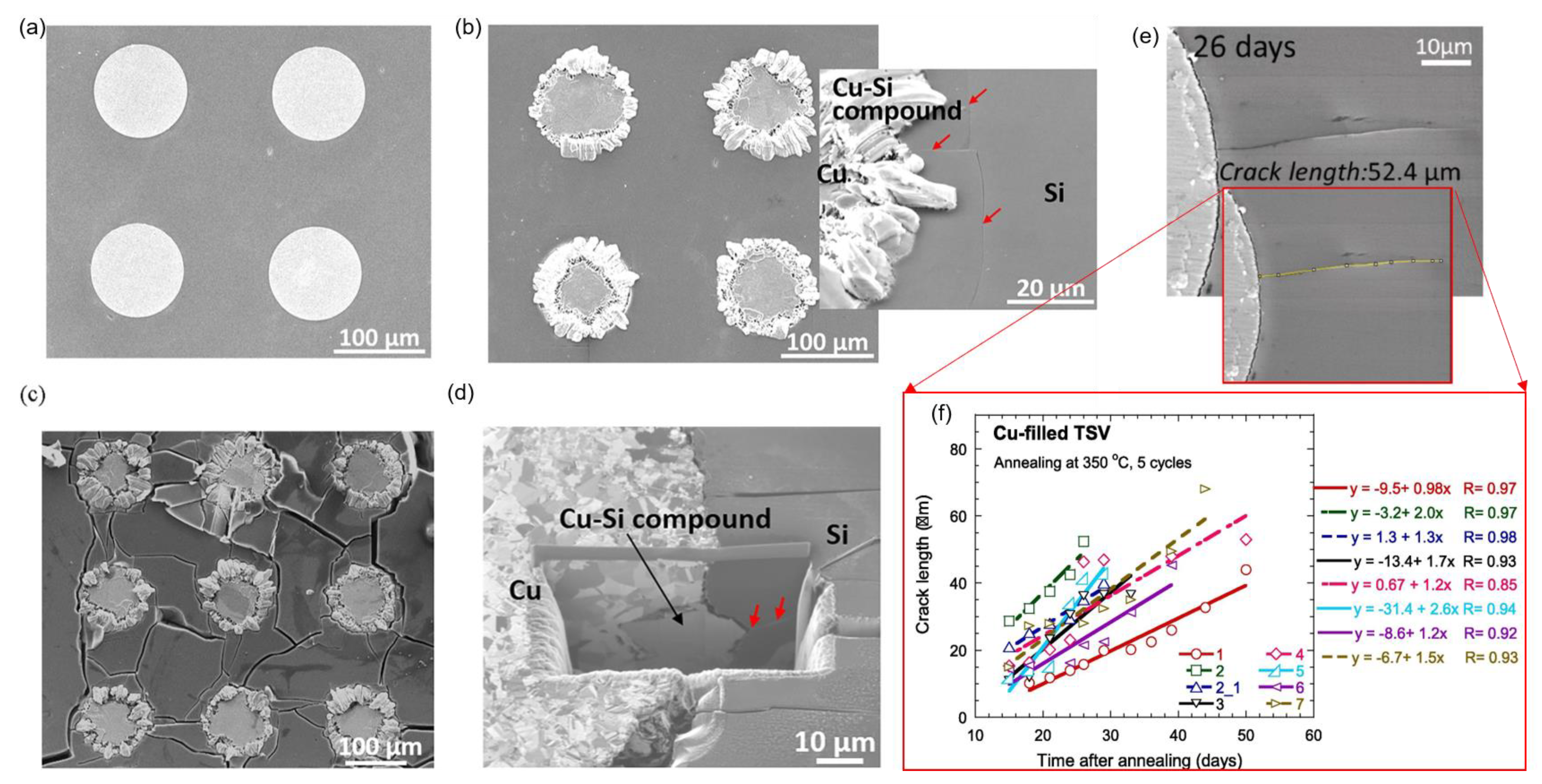
The key challenge associated with the long-term structural reliability of TSV technology stems are the different thermal expansion coefficients (CTEs) of Cu (17.5 × 10⁻⁶ K−1) and Si (2.6 × 10⁻⁶ K−1), which can lead to thermal stresses in these structures during thermal excursion of microelectronic devices [7,47]. The presence of large thermal stresses in TSV structures can be particularly detrimental to silicon, which is a brittle material. If the thermal stresses exceed the strength of the silicon, it can lead to cracks and fractures that can compromise the performance and reliability of the IC. Furthermore, the fracture of the Si−Cu interface can cause delamination, which can also lead to performance and reliability issues. The study by Kumar et al. [7] examined the fracture of Si wafers in CF-TSV caused by annealing in the temperature range of 250–550 °C and natural aging after annealing. They observed the nucleation of microcracks in Si near the Cu column, which propagated at a constant rate during post-annealing room temperature aging, thus, confirming delayed fracture in Si. Microstructural examination showed that the microcracks were the result of Cu-Si compounds formed during the annealing process and that the cracks were caused by Si oxidation at the crack tips’ extension (Figure 9) [48,49].
Initially, silicon (Si) reacts with oxygen to form a layer of silica, which subsequently experiences fracture due to slow crack growth following the mechanism proposed by Wiederhorn [48]. Moreover, the failure of micrometer-thick polysilicon films under fatigue loading and environmental conditions can be attributed to the thickening of the oxide layer and subsequent fracture. This fracture occurs due to a subcritical crack extension induced by moisture within the oxide layer. The oxidation of Si primarily occurs in a narrow region along the crack, leading to the reasonable assumption that Si undergoes oxidation only near the crack tip. The presence of Cu−Si compounds results in consistently high residual stress at the crack tip, thereby significantly accelerating oxidation kinetics. As the average free velocity of oxygen under ambient conditions is 480 m/s, the supply of oxygen to the crack tip does not pose a limiting factor influencing the relatively rapid rate of slow crack extension in CF-TSV samples.
The influence of temperature on protrusion is more pronounced compared to that of annealing time. Additionally, the impact of annealing temperature on residual stresses in the TSV structure is significant. Higher annealing temperatures give rise to increased stresses and deformations, both at elevated temperatures and at room temperature. When the annealing temperature surpasses 350 °C, the protrusion height experiences a sharp increase. This occurs because, under the constraint of the surrounding Si substrate, the Cu can only expand continuously and vertically as the annealing temperature rises. The significant coefficient of thermal expansion (CTE) mismatch between Si and Cu generates greater stresses in the Cu as the TSV undergoes heat treatment. At a sufficiently high temperature, when the thermal stress in the Cu TSV exceeds the yield stress of Cu, irreversible and permanent plastic deformation occurs. Consequently, the Cu material extrudes from the TSV structure. Upon cooling the wafer to room temperature, the elastic deformation recovers, but the irreversible and permanent deformation in the Cu material remains, preventing it from returning to its original shape or length. Thus, a Cu protrusion forms, disrupting the electrical connection of the device and resulting in the failure of the substrate protrusion.
When 3D ICs structures undergo thermal cycling during the processing stage, it can cause residual mechanical stresses to form in the active silicon region. These mechanical stresses have the potential to alter the carrier mobility in the active silicon, which ultimately impacts the device’s performance. The degree to which mechanical stresses and carrier mobility are affected is dependent on the thermal excursions during processing and the physical properties of the constituent materials. It is also worth noting that during the formation of Cu-Si compounds, which occurs when copper diffuses into the silicon, a large compressive stress is generated in the silicon. This stress can lead to the nucleation of microcracks in the silicon wafer near its sharp edges. Over time, the microcracks in the silicon wafer along the [1 1 0] direction grow slowly, leading to the merging of cracks produced by different TSVs. To prevent or delay the cracking of the diffusion barrier layers, thicker barrier layers, silicon walls with flatter scallops, and lower fabrication and operating temperatures can be implemented. By doing so, the likelihood of microcrack formation and subsequent merging of cracks can be reduced [13].
Figure 9. (a) TSV sample; (b) TSV sample after 550 °C annealing; (c) TSV sample after 550 °C annealing and aging 35 days at room temperature; (d) SEM micrographs showing the top view of an array of CF−TSV after annealing at 450 °C after 70 days of natural ageing; (e) SEM micrograph showing the procedure used for measuring the crack length. (f) Variation in crack length of different surface cracks with the duration of natural ageing (adapted from [7]).
Applsci 13 08301 g009
The current insulating dielectric layer material used in TSV technology is primarily silicon dioxide (SiO2). However, SiO2 has a significant thermal expansion coefficient (CTE) mismatch with copper, which can lead to reliability issues. This mismatch in CTE can trigger various problems, such as copper plastic expansion outwards, interface cracking, silicon substrate rupture, and more. If these problems are not adequately addressed, they can eventually lead to a significant impact on the service life and reliability of the 3D integrated system. The thermal expansion mismatch between SiO2 and copper is a critical issue that needs to be resolved to ensure the long-term reliability of TSV technology. When subjected to temperature changes, the difference in the CTE of SiO2 and copper can result in mechanical stresses that can cause the copper to deform or even crack, leading to a failure of the TSV structure. Furthermore, the thermal expansion mismatch can also cause the SiO2 to crack or delaminate from the copper, leading to additional reliability issues. To overcome these challenges, several alternative materials are being investigated to replace SiO2 as the insulating dielectric layer material. One promising option are low-CTE materials, such as silicon nitride (Si3N4), which can provide a closer match to the CTE of copper and reduce the mechanical stresses on the TSV structure during thermal cycling. Other materials, such as organic polymers and spin-on glasses, are also being investigated as potential candidates for insulating dielectric layers in TSVs.
In conclusion, the mismatch in the thermal expansion coefficient between SiO2 and copper presents a notable challenge in TSV technology. This challenge has the potential to adversely affect the reliability and long-term performance of 3D integrated systems. To overcome this issue and enhance the reliability of TSV structures, researchers are exploring the use of alternative materials with lower coefficients of thermal expansion (CTE). Additionally, the implementation of microfluidic cooling has emerged as a promising solution for 3D ICs with high power density. Since 2012, the US Defense Advanced Research Projects Agency (DARPA) has been actively involved in the development of the Intra-Chip/Inter-Chip Enhanced Cooling (ICECool) thermal packaging program. This program aims to address cooling limitations and overcome significant barriers to further progress in Moore’s Law for electronic components and systems. Microfluidic cooling is employed as an active thermal management technique, enabling direct cooling of heat-generating sites within the chip, substrate, and/or package. By controlling the flow rate in liquid cooling, thermal hot spots can be mitigated while optimizing the overall energy consumption of the cooling system. Minimizing the pressure drop in integrated microchannel cooling networks is a key challenge that needs to be addressed in order to achieve efficient cooling [45,50]. Microfluidic cooling stands out as a highly promising thermal management technology for 3D ICs. However, there are several significant technical challenges that need to be addressed to ensure the widespread adoption of this technology. From a scientific standpoint, it is crucial to gain a comprehensive understanding of the physical properties of liquid–gas phase change processes, with a particular focus on optimizing heat dissipation. This includes exploring scenarios, like thin film evaporation, to maximize the efficiency of heat transfer.

3.3. Stresses

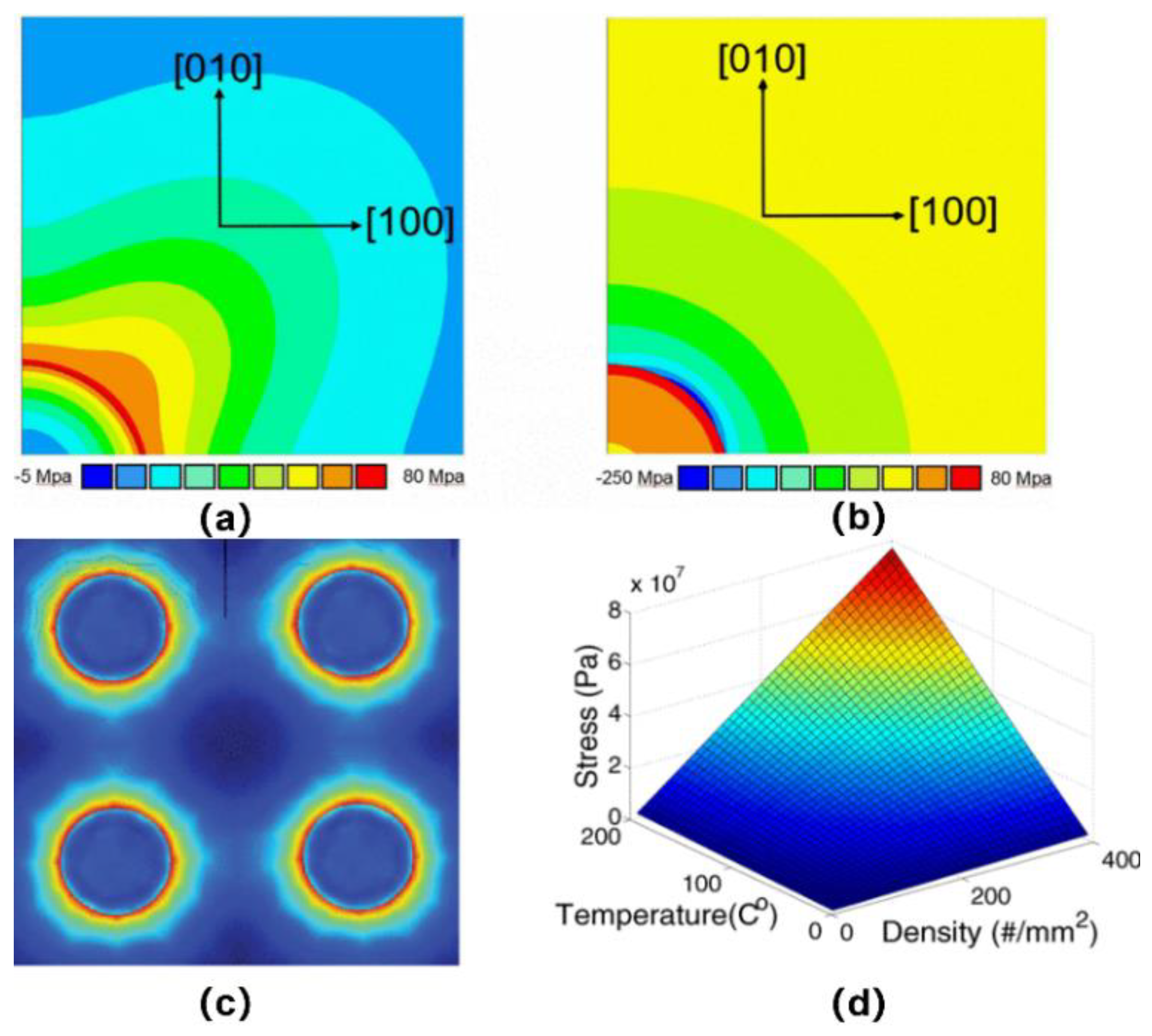
Through heating and cooling processes, the through-silicon via (TSV) undergoes volume changes which can result in induced stresses. The TSV processing temperature is typically higher than the post-operating temperature, leading to residual stresses that can impact both the silicon and the TSV. The magnitude of the induced stresses in the TSV depends on several factors, including the diameter of the TSV and the difference between the processing and operating temperatures. Larger TSV diameters tend to have greater stress magnitudes because the equivalent force and deformation increase as the distance from the center of the TSV to the edge of the silicon increases [28] (Figure 10). This residual stress can lead to delamination and even cracking during the lifetime of the component, which can lead to the failure of the entire integrated system [51]. The through-silicon via (TSV) copper experiences elasto-plastic deformation and creep during the manufacturing process, which exposes it to high thermal loads. As a result, the stress distribution during the service process may differ significantly from the previous process, which leaves behind thermal residual stresses that do not cause deformation at stress-free temperatures. Moreover, different components of the IC have distinct thermal residual stresses due to variations in their package flatness planarity (PFP), thermal loads, locations, and structures, as well as elasto-plastic deformation mechanisms. PFP-induced thermal residual stresses can substantially impact the TSV’s future deformation [13,18,31].
Residual stresses are an important factor that affects the shape, size, and performance of devices, especially integrated devices (IDs) and micro-electromechanical systems (MEMS). These systems may undergo plastic deformation when subjected to thermal residual stresses that exceed the yield strength of the material. Additionally, when thermal residual stress surpasses the material limit, it may lead to crack formation and growth, which is highly undesirable. Therefore, it is crucial to reduce and eliminate thermal residual stresses to improve the mechanical properties and service life of these devices. To achieve this, optimizing the distribution of residual stresses by properly controlling the package flatness planarity, shape, and size of the ID can extend the mechanical properties and service life. Researchers have also investigated the relationship between residual stresses and fatigue life, focusing on improving the relationship between residual stresses and the PFP. Furthermore, analyzing and optimizing the PFP of 3D integrated circuits (ICs) can be performed through an effective and convenient finite element method. By utilizing this method, it is possible to achieve optimal PFP and improve the performance and longevity of the 3D ICs. Therefore, understanding and controlling residual stresses is critical to ensuring the reliable and efficient operation of microsystems, IDs, and MEMS [18,52].
Figure 10. (a) Radial stresses around a TSV; (b) circumferential stresses around a TSV [51]; (c) variation in TSV stress with distance; (d) variation in TSV stress with temperature and TSV density [53].
Applsci 13 08301 g010
In addition, due to its higher coefficient of thermal expansion (CTE), copper mainly generates tensile radial stresses within the silicon, while compressive circumferential stresses occur within the silicon. Consequently, the interface between the TSV and the silicon substrate experiences the highest stresses, making it the most vulnerable to failure. The stress distribution also exhibits quadruple symmetry due to the cubic symmetry of the silicon crystal. At higher temperatures, such as during TSV annealing, copper expands, resulting in increased compressive stresses around the TSV laterally and additional pumping out along the TSV towards the chip surface. This can cause additional stresses and potentially delaminate the functional layers atop the TSV. However, annealing and chemical mechanical polishing (CMP) of the copper protrusions can mitigate this effect.
Moreover, the radial and circumferential stresses generated by the CTE mismatch between the copper and silicon also impact the mechanical and electrical properties of the TSVs. For instance, the tensile radial stresses in copper can cause void formation, which can lead to the degradation of TSV electrical performance. Additionally, the compressive circumferential stresses can influence the mechanical strength of TSVs and their adhesion to the silicon substrate [7,51,54].
Due to the small size of through-silicon vias (TSVs), it is crucial to use microscopic characterization techniques to test their reliability. Although several experimental methods have been employed to analyze the stress distribution on TSVs, including micro-Raman spectroscopy and synchrotron X-ray microdiffraction techniques, these techniques tend to be expensive and have limitations. In contrast, numerical simulations are a popular and cost-effective method for evaluating the reliability of TSVs, such as using finite element analysis [35,55]. One study conducted by Kim et al. [14] found that the silicon near Cu TSVs undergoes significant stresses during processing steps. To characterize the local stress of Si around Cu TSVs of sizes ranging from 4 to 8 μm, micro-Raman spectroscopy was utilized as a function of processing steps. The measured stresses were then used to determine the keep-off-zone that can be used in device design to ensure reliability. It is worth noting that the Raman displacement is proportional to the sum of the stresses. Therefore, even if the actual stress is relatively high, it may lead to a low Raman shift. Hence, assuming that the region has no stress due to the low Raman shift is incorrect and can result in inaccurate predictions. It is important to verify finite element simulations of stress distribution in TSVs by conducting micro-Raman spectroscopy and vice versa. By generating a model and using appropriate material data, finite element analysis can be used to simulate the stress behavior in a chip with integrated TSV. With numerical simulations, it is possible to assess the reliability issues of TSVs without incurring significant costs or limitations, unlike experimental methods, such as micro-Raman spectroscopy and synchrotron X-ray microdiffraction techniques. In addition to the conventional methods mentioned above, an ion beam delamination (ILR) method was proposed by Si Chen et al. to determine the residual stresses at the TSV-Cu/TiW/SiO2/Si interface on the nanoscale [56]. This method measures the corresponding deflection δ(t) from a high magnification SEM image of the microcantilever tip region, calculates the curvature κ from the microcantilever length and the original cantilever deflection δoriginal, and then solves for the stress gradient. Additionally, Cho et al. introduced optical second-harmonic generation (SHG) scanning microscopy to characterize strain fields around TSVs while maintaining micrometer spatial resolution [57].

3.4. Noise Coupling

One of the major challenges of TSVs is their signal integrity (SI) characteristics, particularly coupling. TSVs have a relatively large diameter and are suspended in a low-resistance silicon substrate with only a thin layer of oxide (known as a TSV liner) separating them from the substrate. This thin oxide liner and the large TSV surface area result in significant capacitance between the TSV and the substrate. As a result, signal coupling occurs from the TSV into the substrate and then to other TSVs. The diameter of the TSV and the thickness of the liner are determined by the manufacturing process and cannot be easily altered. Thus, designers must consider design techniques to handle the low-impedance coupling path between TSVs. Failure to address noise coupling may cause a circuit to malfunction or degrade its performance in several ways. It is important to consider TSV fabrication techniques for power–noise coupling during service. Typical TSV parameters with noise trends using different fabrication techniques are presented in Table 2. The power supply noise in TSV-based 3-D ICs increases with the scaling of CMOS technology. This trend occurs because the current density within each layer and the operating frequency of 3-D ICs tend to increase as CMOS technology scales. With the same TSV technology and distribution conditions, larger currents pass through each P/G TSV, resulting in higher levels of on-chip power supply noise in 3D ICs.
The noise signal ratio due to on-chip inductance is increasing due to increased switching speeds, reduced spacing between interconnects, and reduced device noise tolerance. The effects of this noise, such as oscillation, overshoot, and downshoot, make chip performance a concern in design. The effects of crosstalk-induced overshoot and undershoot generated at noisy sites can propagate false switches and generate logic errors. False switching occurs when the overshoot or downshoot amplitude exceeds the threshold. The peak overshoot and undershoot generated by the noise field can wear away the thin gate oxide layer and lead to permanent chip failure. As the line resistance increases, the noise peak decreases. As the width of the PMOS driver increases, the victim line is more susceptible to crosstalk noise. The crosstalk level increases substantially with increasing driver width, as shown in Table 2.
Table 2. Typical parameters for different TSV fabrication technologies [58,59].
ParameterVia-FirstVia-MiddleVia-Last
Diameter (μm)4410
Pitch (μm)8820
Length (μm)106060
TSV resistance (Ω)5.70.90.02
TSV inductance (pH)4.249.834.9
TSV coupling capacitance (fF)1.26.76
For instance, coupling between signal transmission lines may result in changes in the logic value at the transistor gate input, leading to incorrect logic or short-circuit currents. Similarly, coupling between the signal TSV and the power supply TSV can lead to changes in the VDD or GND supply rails, which can increase leakage currents. Furthermore, TSV−TSV coupling may result in the conversion signal changing value too slowly, leading to timing violations. Therefore, to mitigate the adverse effects of coupling, 3D IC designers can implement various design techniques, such as optimizing the power distribution network, utilizing shielded TSVs, and reducing the signal’s rise time. These techniques can help reduce the impact of noise coupling and improve the overall signal integrity of TSVs in 3D ICs [3,60].
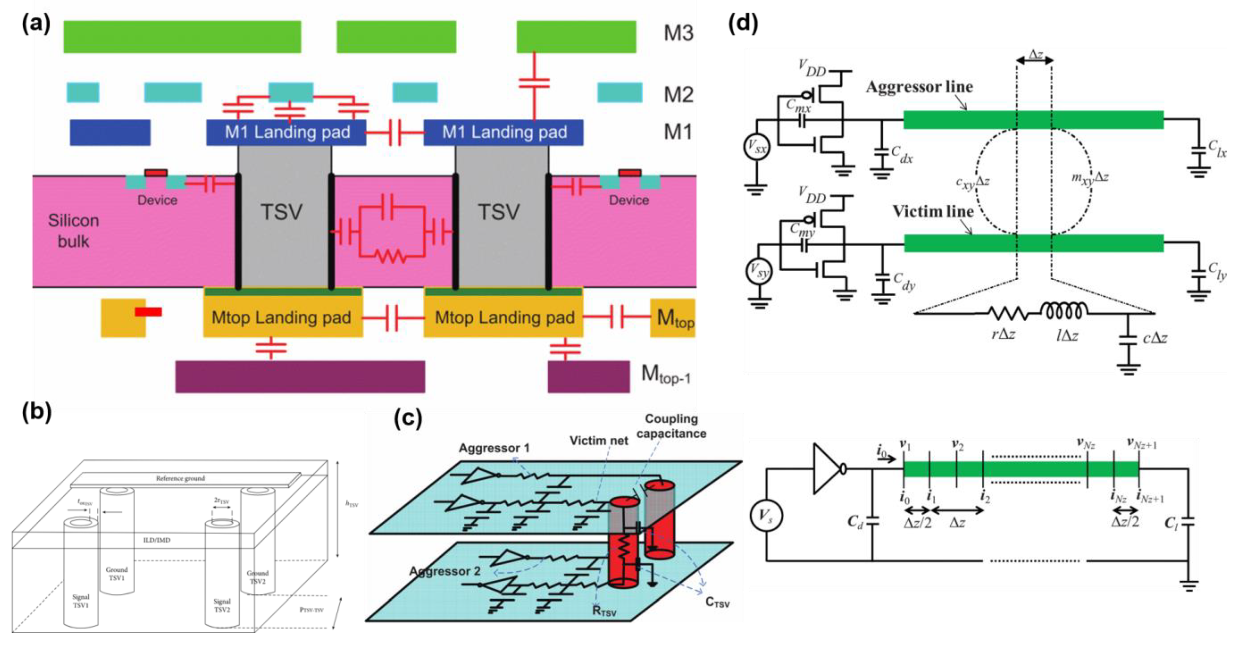
According to the shrinking of CMOS technology CMOS RF/mixed signals is the leading response for moderate cost, moderate power, and extreme functionality and provides higher performance. However, circuit sizes are becoming tremendous and enlarging the noise of digital circuits. As such, it is observed that digital noise leaks from RF circuits to the substrate, which will decrease the RF circuit’s performance. The important choice is to enhance the noise among digital and RF circuits. From all this observation, researchers made use of electrode materials for the surface layer of the TSV and a copper material for the outer layer and then verified the results [61]. Kumar et al. [62,63] provided an accurate model for the dynamic crosstalk analysis of coupled multiple on-chip interconnects driven by CMOS inverters. The proposed model is developed using the finite difference time domain (FDTD) technique for coupled RLC interconnects, whereas the alpha power law model is used to represent the transistors in a CMOS driver. Over the random number of test cases, crosstalk-induced peak voltage and propagation delay show average errors of 1.1% and 4.3%, respectively, with respect to HSPICE results. The finite-difference time-domain (FDTD, Figure 11d)) technique is widely used to solve electromagnetic wave problems. It is a fast, accurate, and powerful technique involving the discretization of electromagnetic fields in the time domain [64]. Several researchers have proposed various improved FDTD techniques to overcome CFL stability criteria based on different algorithms, such as alternating direction implicit FDTD, stepwise FDTD, and Crank–Nicolson FDTD; Kumar et al. argue that large-scale integrated (VLSI) interconnects are driven and terminated by nonlinear CMOS drivers and capacitive loads, respectively. Therefore, the existing unconditionally stable FDTD (US-FDTD) technique is not suitable for analyzing the performance of VLSI interconnects. They developed a new model in which the interconnects are driven by nonlinear CMOS drivers that are modeled by an improved alpha power-law model that includes drain conductance parameters [64,65].
Figure 11. (a) An illustration of TSV-related coupling; (b) structure of the TSV-TSV coupling noise; (c) an illustration of the 3D victim net; (d) schematic of coupled interconnects driven by CMOS drivers and the representation of space discretization of an interconnect line for the US-FDTD technique. (adapted from [1,64,66]).
Applsci 13 08301 g011
To reduce the degree of cross-coupling between TSVs, a shield can be inserted between them. This shield can be made of any metal piece that hinders the propagation of electromagnetic waves. However, optimizing the placement of the shield requires more work. Previous studies on TSV coupling have mainly presented circuit models of the coupling phenomenon.
For instance, in a study published in [67], the authors proposed a TSV noise coupling model based on the three-dimensional transmission line matrix method (3D-TLM). This model allows for the estimation of the noise coupling transfer functions from TSV to TSV and from TSV to active circuits in a complex 3D structure. In another study published in [68], the authors examined the parasitic substrate coupling effects in 3D-ICs caused by TSVs. They performed electrical characterization by studying some test structures to extract the electrical model of substrate coupling with RF signals. In [69], the authors presented an equivalent circuit model for differential TSV pairs. They calculated and analyzed the key differential characteristics based on the aggregate circuit model of multiple TSVs. However, circuit models are very accurate but take a long time to solve because they require solving a system of differential equations.
Therefore, to speed up the optimization process during chip-level shield placement, Liu and Serafy et al. [1,3,66,70] proposed geometric models for TSV cross-coupling. These models can be quickly solved, unlike circuit models. In [1], the authors proposed an intelligent method based on genetic algorithms (GAs) and a recent particle swarm optimization (PSO) heuristic model to identify the parameters of TSV-TSV and TSV–contact noise coupling in 3D IC design. Both models included equivalent circuits for TSV, RDL (redistribution layer), metal interconnects, and substrates.
Modeling TSV structures and simulating them in the time domain is one of the most critical issues in this field. Thus, future research should focus on developing more accurate and efficient modeling and simulation techniques to address the challenges posed by TSV coupling in 3D IC design [71,72].

4. Outlook

4.1. New Etching Techniques

The ever-increasing integration of integrated circuits demands TSVs with smaller feature sizes and diameters. However, the conventional TSV etching process is inadequate for future integrated circuits with feature sizes smaller than 3 nm. Therefore, researchers are exploring new etching techniques to realize TSV fabrication. Chemical or physicochemical combinations are promising approaches for TSV etching, which are expected to replace the traditional single etch mode. Several research groups are working on developing new etching techniques, such as using magnetic fields to attract metal catalysts deposited on silicon surfaces for faster etch speeds when fabricating high-magnification grating structures. In addition, thermal atomic layer etching is a viable solution for atomically accurate material removal and TSV fabrication on a very small scale.
Furthermore, TSVs are not only becoming smaller, but also denser. The ever-increasing number of TSVs per unit area poses new challenges to TSV fabrication techniques. Therefore, new methods for controlling the depth and diameter of TSVs are being explored. For example, high-speed plasma beams can be used to etch TSVs with a high aspect ratio and uniform diameter. Moreover, novel materials with improved thermal and electrical properties are being investigated to enhance TSV performance and reduce power consumption. For instance, researchers are exploring the use of graphene, carbon nanotubes [73,74], and other 2D materials [75] as TSV liners and interconnects due to their high thermal conductivity and excellent electrical properties.
In addition to new etching techniques and materials, TSV reliability and quality assurance are critical factors for successful 3D IC integration. Non-destructive metrology techniques have been developed to measure TSV dimensions, integrity, and filling defects. Moreover, advanced simulation tools, including finite element methods and artificial intelligence and machine learning, are used to predict and optimize TSV performance, reliability, and yield. However, there is still a need for complete design tools and methodologies to address the challenges posed by TSV fabrication and integration in 3D ICs. Therefore, further research is needed to develop robust and efficient TSV fabrication processes, quality control techniques, and design methodologies to enable the realization of advanced 3D ICs [22,23,76].

4.2. New Design Tools and Approaches

As the integration of integrated circuits increases, the use of 3D-ICs has become popular due to its capability of stacking multiple chips together vertically, resulting in a higher transistor density with reduced interconnect power and latency. However, this approach comes with several challenges that must be considered during the design process. The increased interconnect complexity poses a risk to signal integrity, and the noise coupling between TSVs, signal delays caused by thermal-electrical coupling, and the effects of stress on carriers must be taken into account. Furthermore, global routing has become a critical aspect, and the optimization of the cost function with layer assignments based on dynamic programming is essential to achieve less overflow and fast convergence [77,78].
The electrical state of TSVs is coupled with multiple physical domains, and highly inhomogeneous power densities and large temperature gradients must be avoided. Additionally, the coefficients of thermal expansion of the TSV material and the substrate material may introduce large mechanical stresses, leading to delay variations in the driver through electrical–mechanical coupling [79,80]. Such delay variation may introduce bias for delay-sensitive clock tree designs, and, therefore, a robust physical design in 3D ICs with TSVs requires optimization in terms of coupling in the electrical, mechanical, and thermal domains [20,81,82].
The deployment of signal TSVs across the 3D chip may result in uneven temperature differences, leading to significant clock offsets due to the electrical–thermal coupling of the signal TSVs. The stresses induced by the TSVs may also affect the mobility and latency of the driver, further worsening the clock offsets of the electrical–mechanical coupling of the driver across the 3D chip. Hence, conventional design approaches that do not consider temperature and stress gradients may become inaccurate and unreliable. Thus, there is a need for new design tools and methods to handle these issues.
We have collected some new TSV performance with the new manufacturing process, as shown in Table 3.
Table 3. TSV parameters under different new processes.
hTSVRTSVEquivalent CircuitInsertion Loss S21Reference
MW-CNT TSV100 μm10 μmApplsci 13 08301 i001−0.1 dB
(20 GHz)
[83]
Elliptic cylindrical TSV60 μm2.5 μm
7.5 μm
−0.6 dB (20 GHz)[84]
CMF-TSV100 μm10 μmApplsci 13 08301 i002−16.8 dB (3.5 GHz)[85]
Tapered TSV50 μm0.17 μm (min)
0.52 μm (max)
Applsci 13 08301 i003−0.18 dB (20 GHz)[86]
PI-TSV300 μm30 μmApplsci 13 08301 i004−2.63 dB (2.4 GHz)[87]
32 nm with regard to TSV9.6 μm2 μmApplsci 13 08301 i00532.16% improvement (20 GHz)[88]

5. Conclusions

3D integration with through-silicon vias (TSVs) is a promising candidate to perform system-level integration with smaller package size, higher interconnection density, and better performance. TSV fabrication is the key technology to permit communications between various strata of the 3D integration system. This review delves into the various methods employed for measuring the geometry and electrical properties of TSVs, as well as the potential reliability issues associated with TSVs in 3D integrated circuits. Currently, measurements of TSVs primarily focus on the geometry of the TSV, including any filling defects and the integrity of the insulating dielectric liner. However, the risks associated with TSV reliability in service are primarily due to copper contamination, thermal fields, stress fields, and noise coupling between TSVs. In particular, the coupling between several physical fields poses a significant challenge to the design of 3D-ICs with TSVs. As a result, there is a pressing need for comprehensive design tools and methods in this area. To address these issues, numerical simulations based on finite element methods, as well as artificial intelligence and machine learning, have been applied to this field. However, there is still much work to accomplish to fully understand the potential risks of TSVs in 3D integrated circuits and to optimize their performance. Furthermore, the increased integration of 3D-ICs also presents a significant challenge to the manufacturing process of TSVs.

Author Contributions

Conceptualization, J.W.; investigation, F.D. and Z.L.; data curation, S.C.; writing—original draft preparation, J.W.; writing—review and editing, F.D. and H.C.; visualization, J.W.; supervision, J.L.; project administration, H.C. and X.Y. All authors have read and agreed to the published version of the manuscript.

Funding

This work was supported in part by the Key-Area Research and Development Program of Guangdong Province under Grant 2022B0701180002 and supported by supported by the CEPREI Innovation and Development Fund No. 22Z04.

Institutional Review Board Statement

We confirm that the manuscript has been read and approved by all named authors.

Informed Consent Statement

The authors agree to publication in The International Journal of Advanced Manufacturing Technology.

Data Availability Statement

The data sets supporting the results of this article are included within the article and its additional files.

Conflicts of Interest

The authors declare that they have no conflict of interest.

References

  1. Belaid, K.A.; Belahrach, H.; Ayad, H. Genetic Algorithms and Particle Swarm Optimization Mechanisms for Through-Silicon Via (TSV) Noise Coupling. Appl. Comput. Intell. Soft Comput. 2021, 2021, 1–14. [Google Scholar] [CrossRef]
  2. Lin, P.; Xie, X.; Wang, Y.; Lian, B.; Zhang, G. A multi-step etch method for fabricating slightly tapered through-silicon vias based on modified Bosch process. Microsyst. Technol. 2018, 25, 2693–2698. [Google Scholar] [CrossRef]
  3. Serafy, C.; Shi, B.; Srivastava, A. A geometric approach to chip-scale TSV shield placement for the reduction of TSV coupling in 3D-ICs. Integration 2014, 47, 307–317. [Google Scholar] [CrossRef]
  4. Vianne, B.; Richard, M.-I.; Escoubas, S.; Labat, S.; Schülli, T.; Chahine, G.; Fiori, V.; Thomas, O. Through-silicon via-induced strain distribution in silicon interposer. Appl. Phys. Lett. 2015, 106, 141905. [Google Scholar] [CrossRef]
  5. Luo, J.; Sun, Y.; Wang, B.; Jin, Z.; Yang, S.; Wang, Y.; Ding, G. Elastic and elastic-plastic analysis of multilayer thin films filled with heterogeneous materials. AIP Adv. 2018, 8, 115134. [Google Scholar] [CrossRef] [Green Version]
  6. Lau, J.H. Overview and outlook of through-silicon via (TSV) and 3D integrations. Microelectron. Int. 2011, 28, 8–22. [Google Scholar] [CrossRef]
  7. Sonawane, D.; Kumar, P. New insights into fracture of Si in Cu-filled through silicon via during and after thermal annealing. Eng. Fract. Mech. 2020, 238, 107281. [Google Scholar] [CrossRef]
  8. Lai, M.-F.; Li, S.-W.; Shih, J.-Y.; Chen, K.-N. Wafer-level three-dimensional integrated circuits (3D IC): Schemes and key technologies. Microelectron. Eng. 2011, 88, 3282–3286. [Google Scholar] [CrossRef]
  9. Wang, X.; Chen, D.; Li, D.; Kou, C.; Yang, Y. The Development and Progress of Multi-Physics Simulation Design for TSV-Based 3D Integrated System. Symmetry 2023, 15, 418. [Google Scholar] [CrossRef]
  10. Gambino, J.P.; Adderly, S.A.; Knickerbocker, J.U. An overview of through-silicon-via technology and manufacturing challenges. Microelectron. Eng. 2015, 135, 73–106. [Google Scholar] [CrossRef]
  11. Yoon, H.; Choi, K.-S.; Bae, H.-C.; Moon, J.-T.; Eom, Y.-S.; Jeon, I. Evaluating the material properties of underfill for a reliable 3D TSV integration package using numerical analysis. Microelectron. Reliab. 2017, 71, 41–50. [Google Scholar] [CrossRef]
  12. Knechtel, J.; Sinanoglu, O.; Elfadel, I.M.; Lienig, J.; Sze, C.C.N. Large-Scale 3D Chips: Challenges and Solutions for Design Automation, Testing, and Trustworthy Integration. IPSJ Trans. Syst. LSI Des. Methodol. 2017, 10, 45–62. [Google Scholar] [CrossRef] [Green Version]
  13. Karmarkar, A.P.; Xu, X.; El Sayed, K.; Guo, W.; Van der Plas, G.; Van Huylenbroeck, S.; Gonzalez, M.; Absil, P.; Beyne, E. Modeling Copper Plastic Deformation and Liner Viscoelastic Flow Effects on Performance and Reliability in Through Silicon Via (TSV) Fabrication Processes. IEEE Trans. Device Mater. Reliab. 2019, 19, 642–653. [Google Scholar] [CrossRef]
  14. Kim, J.H.; Yoo, W.S.; Han, S.M. Non-destructive micro-Raman analysis of Si near Cu through silicon via. Electron. Mater. Lett. 2017, 13, 120–128. [Google Scholar] [CrossRef]
  15. Frank, T.; Moreau, S.; Chappaz, C.; Leduc, P.; Arnaud, L.; Thuaire, A.; Chery, E.; Lorut, F.; Anghel, L.; Poupon, G. Reliability of TSV interconnects: Electromigration, thermal cycling, and impact on above metal level dielectric. Microelectron. Reliab. 2012, 53, 17–29. [Google Scholar] [CrossRef]
  16. Barnes, J.-P.; Djomeni, L.; Minoret, S.; Mourier, T.; Fabbri, J.-M.; Audoit, G.; Fadloun, S. Focused ion beam time-of-flight secondary ion mass spectroscopy tomography of through-silicon vias for 3D integration. J. Vac. Sci. Technol. B 2016, 34, 03H137. [Google Scholar] [CrossRef]
  17. Bea, J.; Lee, K.; Fukushima, T.; Tanaka, T.; Koyanagi, M. Evaluation of Cu Diffusion from Cu Through-Silicon Via (TSV) in Three-Dimensional LSI by Transient Capacitance Measurement. IEEE Electron Device Lett. 2011, 32, 940–942. [Google Scholar] [CrossRef]
  18. Sun, Y.; Sun, S.; Zhang, Y.; Luo, J.; Wang, Y.; Ding, G.; Jin, Y. Initial thermal stress and strain effects on thermal mechanical stability of through silicon via. Microelectron. Eng. 2016, 165, 11–19. [Google Scholar] [CrossRef]
  19. Nabil, A.; Bernardo, J.A.; Ma, Y.; Abouelatta, M.; Shaker, A.; Bouchet, L.F.; Ragai, H.; Gontrand, C. Electrical modeling of tapered TSV including MOS-Field effect and substrate parasitics: Analysis and application. Microelectron. J. 2020, 100, 104797. [Google Scholar] [CrossRef]
  20. Xiao, H.; He, H.; Ren, X.; Zeng, P.; Wang, F. Numerical modeling and experimental verification of copper electrodeposition for through silicon via (TSV) with additives. Microelectron. Eng. 2017, 170, 54–58. [Google Scholar] [CrossRef]
  21. Jung, D.H.; Kim, Y.; Kim, J.J.; Kim, H.; Choi, S.; Song, Y.-H.; Bae, H.-C.; Choi, K.-S.; Piersanti, S.; de Paulis, F.; et al. Through Silicon Via (TSV) Defect Modeling, Measurement, and Analysis. IEEE Trans. Compon. Packag. Manuf. Technol. 2017, 7, 138–152. [Google Scholar] [CrossRef]
  22. Guo, H.; Cao, S.; Li, L.; Zhang, X. A review on the mainstream through-silicon via etching methods. Mater. Sci. Semicond. Process. 2022, 137, 106182. [Google Scholar] [CrossRef]
  23. Fursenko, O.; Bauer, J.; Marschmeyer, S.; Stoll, H.-P. Through silicon via profile metrology of Bosch etching process based on spectroscopic reflectometry. Microelectron. Eng. 2015, 139, 70–75. [Google Scholar] [CrossRef]
  24. Shen, W.-W.; Chen, K.-N. Three-Dimensional Integrated Circuit (3D IC) Key Technology: Through-Silicon Via (TSV). Nanoscale Res. Lett. 2017, 12, 56. [Google Scholar] [CrossRef] [Green Version]
  25. Ehsan, M.A.; Zhou, Z.; Yi, Y. Electrical modeling and analysis of sidewall roughness of through silicon vias in 3D integration. In Proceedings of the IEEE International Symposium on Electromagnetic Compatibility (EMC), Raleigh, NC, USA, 4–8 August 2014; pp. 52–56. [Google Scholar]
  26. Zhou, J.; Wan, L.; Dai, F.; Wang, H.; Song, C.; Du, T.; Chu, Y.; Pan, M.; Guidotti, D.; Cao, L.; et al. Accurate electrical simulation and design optimization for silicon interposer considering the MOS effect and eddy currents in the silicon substrate. In Proceedings of the IEEE 62nd Electronic Components and Technology Conference, San Diego, CA, USA, 29 May–1 June 2012; pp. 658–664. [Google Scholar]
  27. Li, Y.; Srinath, P.K.M.; Goyal, D. A Review of Failure Analysis Methods for Advanced 3D Microelectronic Packages. J. Electron. Mater. 2015, 45, 116–124. [Google Scholar] [CrossRef]
  28. Pan, Y.; Li, F.; He, H.; Li, J.; Zhu, W. Effects of dimension parameters and defect on TSV thermal behavior for 3D IC packaging. Microelectron. Reliab. 2017, 70, 97–102. [Google Scholar] [CrossRef]
  29. Peng, B.; Hou, W.; Xu, Q. Precision 3D profile in-line measurement of through-silicon via (TSV) based on high-frequency spectrum signals in the pupil plane. Opt. Commun. 2018, 424, 107–112. [Google Scholar] [CrossRef]
  30. Huang, Y.-J.; Pan, C.-L.; Lin, S.-C.; Guo, M.-H. Machine-Learning Approach in Detection and Classification for Defects in TSV-Based 3-D IC. IEEE Trans. Compon. Packag. Manuf. Technol. 2018, 8, 699–706. [Google Scholar] [CrossRef]
  31. Yi, M.; Bian, J.; Ni, T.; Jiang, C.; Chang, H.; Liang, H. A Pulse Shrinking-Based Test Solution for Prebond Through Silicon via in 3-D Ics. IEEE Trans. Comput. Aided Des. Integr. Circuits Syst. 2019, 38, 755–766. [Google Scholar] [CrossRef]
  32. Hsu, C.-L.; Tsai, J.-Y.; Hsueh, T.-J. Novel field emission structure of CuO/Cu2O composite nanowires based on copper through silicon via technology. RSC Adv. 2015, 5, 33762–33766. [Google Scholar] [CrossRef]
  33. Chandrakar, M.; Majumder, M.K. Performance Analysis Using Air Gap Defected Through Silicon Via: Impact on Crosstalk and Power. IEEE Trans. Compon. Packag. Manuf. Technol. 2022, 12, 1832–1840. [Google Scholar] [CrossRef]
  34. Noia, B.; Panth, S.; Chakrabarty, K.; Lim, S.K. Scan Test of Die Logic in 3-D ICs Using TSV Probing. IEEE Trans. Very Large Scale Integr. (VLSI) Syst. 2015, 23, 317–330. [Google Scholar] [CrossRef]
  35. Cheng, Z.; Ding, Y.; Xiao, L.; Yang, B.; Chen, Z. Study on atomic migration of copper through-silicon-vias with Bosch scallops. Microelectron. Reliab. 2021, 123, 114178. [Google Scholar] [CrossRef]
  36. Nie, L.; Huang, Y.; Liu, M. Internal defects inspection of TSV 3D package based on thermal distribution analysis. AIP Adv. 2021, 11, 085312. [Google Scholar] [CrossRef]
  37. Nair, R.K.R.; Pothiraj, S.; Nair, T.R.R.; Cengiz, K. An efficient partitioning and placement based fault TSV detection in 3D-IC using deep learning approach. J. Ambient. Intell. Humaniz. Comput. 2021, 1–14. [Google Scholar] [CrossRef]
  38. Bandyopadhyay, T.; Han, K.J.; Chung, D.; Chatterjee, R.; Swaminathan, M.; Tummala, R. Rigorous Electrical Modeling of Through Silicon Vias (TSVs) With MOS Capacitance Effects. IEEE Trans. Components, Packag. Manuf. Technol. 2011, 1, 893–903. [Google Scholar] [CrossRef]
  39. Kim, K.; Choi, J.; Woo, S.; Cho, J.; Ahn, S. E-field induced keep-out zone determination method of through-silicon vias for 3-D ICs. Microelectron. Reliab. 2019, 98, 161–164. [Google Scholar] [CrossRef]
  40. Monticeli, F.M.; Shiino, M.Y.; Voorwald, H.J.C.; Cioffi, M.O.H. The synergy effect of carbon/glass/epoxy hybrid laminate in Mode I delamination: A physical microfracture analysis. Eng. Fract. Mech. 2020, 239, 107295. [Google Scholar] [CrossRef]
  41. Li, Y.; Van Huylenbroeck, S.; Roussel, P.; Brouri, M.; Gopinath, S.; Anjos, D.M.; Thorum, M.; Yu, J.; Beyer, G.P.; Beyne, E.; et al. Dielectric liner reliability in via-middle through silicon vias with 3 Micron diameter. Microelectron. Eng. 2016, 156, 37–40. [Google Scholar] [CrossRef]
  42. Frank, T.; Chappaz, C.; Leduc, P.; Arnaud, L.; Lorut, F.; Moreau, S.; Thuaire, A.; El Farhane, R.; Anghel, L. Resistance increase due to electromigration induced depletion under TSV. In Proceedings of the International Reliability Physics Symposium, Monterey, CA, USA, 10–14 April 2011; pp. 3F.4.1–3F.4.6. [Google Scholar] [CrossRef]
  43. Chang, N.; Chung, C.K.; Wang, Y.-P.; Lin, C.F.; Su, P.; Shih, T.; Kao, N.; Hung, J. 3D Micro Bump Interface Enabling Top Die Interconnect to True Circuit Through Silicon Via Wafer. In Proceedings of the IEEE 70th Electronic Components and Technology Conference (ECTC), Orlando, FL, USA, 3–30 June 2020; pp. 1888–1893. [Google Scholar] [CrossRef]
  44. Choi, H.-J.; Choi, S.-M.; Yeo, M.-S.; Cho, S.-D.; Baek, D.-C.; Park, J. An experimental study on the TSV reliability: Electromigration (EM) and time dependant dielectric breakdown (TDDB). In Proceedings of the IEEE International Interconnect Technology Conference, San Jose, CA, USA, 4–6 June 2012; pp. 1–3. [Google Scholar] [CrossRef]
  45. Salvi, S.S.; Jain, A. A Review of Recent Research on Heat Transfer in Three-Dimensional Integrated Circuits (3-D ICs). IEEE Trans. Compon. Packag. Manuf. Technol. 2021, 11, 802–821. [Google Scholar] [CrossRef]
  46. Shin, Y.; Kim, S.E.; Kim, S. Thermal assessment of copper through silicon via in 3D IC. Microelectron. Eng. 2016, 156, 2–5. [Google Scholar] [CrossRef]
  47. Zhao, X.; Ma, L.; Wang, Y.; Guo, F. Effect of Thermal Mechanical Behaviors of Cu on Stress Distribution in Cu-Filled Through-Silicon Vias Under Heat Treatment. J. Electron. Mater. 2017, 47, 142–147. [Google Scholar] [CrossRef]
  48. Song, M.; Wei, Z.; Wang, B.; Chen, L.; Szpunar, J.A. Study on copper protrusion of through-silicon via in a 3-D integrated circuit. Mater. Sci. Eng. A 2019, 755, 66–74. [Google Scholar] [CrossRef]
  49. Zhao, X.; Ma, L.; Wang, Y.; Guo, F. Mechanism of the Local Cu Protrusion in Cu-Filled Through Silicon Vias Under Heat Treatment. J. Electron. Mater. 2018, 48, 152–158. [Google Scholar] [CrossRef]
  50. Wang, S.; Yin, Y.; Hu, C.; Rezai, P. 3D Integrated Circuit Cooling with Microfluidics. Micromachines 2018, 9, 287. [Google Scholar] [CrossRef] [PubMed] [Green Version]
  51. Stiebing, M.; Vogel, D.; Steller, W.; Wolf, M.; Wunderle, B. Challenges in the reliability of 3D integration using TSVs. In Proceedings of the 16th International Conference on Thermal, Mechanical and Multi-Physics Simulation and Experiments in Microelectronics and Microsystems, Budapest, Hungary, 19–22 April 2015. [Google Scholar]
  52. Lee, W.-C.; Min, B.-W.; Kim, J.C.; Yook, J.-M. Silicon-core Coaxial Through Silicon Via for Low-loss RF Si-interposer. IEEE Microw. Wirel. Components Lett. 2017, 27, 428–430. [Google Scholar] [CrossRef]
  53. Sai, M.P.D.; Hao, Y.; Yang, S.; Seng, T.C.; Kyu, L.S. Reliable 3-D Clock-Tree Synthesis Considering Nonlinear Capacitive TSV Model with Electrical–Thermal–Mechanical Coupling. IEEE Trans. Comput. Aided Des. Integr. Circuits Syst. 2013, 32, 1734–1747. [Google Scholar] [CrossRef]
  54. Chen, C.-F.; Wu, S.-T. Equivalent mechanical properties of through silicon via interposers—A unit model approach. Microelectron. Reliab. 2015, 55, 221–230. [Google Scholar] [CrossRef]
  55. Xia, K.; Zhu, Z.; Zhang, H.; Xu, Z. Modeling simplification for thermal mechanical stress analysis of TSV interposer stack. Microelectron. Reliab. 2019, 96, 46–50. [Google Scholar] [CrossRef]
  56. Chen, S.; En, Y.F.; Li, G.Y.; Wang, Z.Z.; Gao, R.; Ma, R.; Zhang, L.X.; Huang, Y. An ion beam layer removal method of determining the residual stress in the as-fabricated TSV-Cu/TiW/SiO2/Si interface on a nanoscale. Microelectron. Reliab. 2020, 112, 113826. [Google Scholar] [CrossRef]
  57. Cho, Y.; Shafiei, F.; Mendoza, B.S.; Lei, M.; Jiang, T.; Ho, P.S.; Downer, M.C. Second-harmonic microscopy of strain fields around through-silicon-vias. Appl. Phys. Lett. 2016, 108, 151602. [Google Scholar] [CrossRef]
  58. Satheesh, S.M.; Salman, E. Power Distribution in TSV-Based 3-D Processor-Memory Stacks. IEEE J. Emerg. Sel. Top. Circuits Syst. 2012, 2, 692–703. [Google Scholar] [CrossRef] [Green Version]
  59. Xu, K.; Friedman, E.G. Scaling trends of power noise in 3-D ICs. Integration 2015, 51, 139–148. [Google Scholar] [CrossRef]
  60. Pragathi, D.; Prasad, D.; Padma, T.; Reddy, P.R.; Kumari, C.U.; Poola, P.K.; Panigrahy, A.K. An extensive survey on reduction of noise coupling in TSV based 3D IC integration. Mater. Today Proc. 2021, 45, 1471–1480. [Google Scholar] [CrossRef]
  61. Kumar, M.S.; Mohanraj, J.; Kumar, N.V.; Valliammai, M. An extensive survey on future direction for the reduction of noise coupling problem in TSV based 3-dimensional IC integration. Mater. Today Proc. 2021, 46, 3502–3511. [Google Scholar] [CrossRef]
  62. Kumar, V.R.; Kaushik, B.K.; Patnaik, A. An accurate model for dynamic crosstalk analysis of CMOS gate driven on-chip interconnects using FDTD method. Microelectron. J. 2014, 45, 441–448. [Google Scholar] [CrossRef]
  63. Kaushik, B.K.; Sarkar, S.; Agarwal, R.P.; Joshi, R.C. Crosstalk analysis of simultaneously switching interconnects. Int. J. Electron. 2009, 96, 1095–1114. [Google Scholar] [CrossRef]
  64. Kumar, V.R.; Alam, A.; Kaushik, B.K.; Patnaik, A. An Unconditionally Stable FDTD Model for Crosstalk Analysis of VLSI Interconnects. IEEE Trans. Compon. Packag. Manuf. Technol. 2015, 5, 1810–1817. [Google Scholar] [CrossRef]
  65. Kaushik, B.K.; Sarkar, S.; Agarwal, R.; Joshi, R. Effect of line resistance and driver width on crosstalk in coupled VLSI interconnects. Microelectron. Int. 2007, 24, 42–45. [Google Scholar] [CrossRef]
  66. Liu, C.; Song, T.; Lim, S.K. Signal integrity analysis and optimization for 3D ICs. In Proceedings of the 12th International Symposium on Quality Electronic Design, Santa Clara, CA, USA, 14–16 March 2011. [Google Scholar]
  67. Cho, J.; Song, E.; Yoon, K.; Pak, J.S.; Kim, J.; Lee, W.; Song, T.; Kim, K.; Lee, J.; Lee, H.; et al. Modeling and Analysis of Through-Silicon Via (TSV) Noise Coupling and Suppression Using a Guard Ring. IEEE Trans. Compon. Packag. Manuf. Technol. 2011, 1, 220–233. [Google Scholar] [CrossRef]
  68. Eid, E.; Lacrevaz, T.; Bermond, C.; Capraro, S.; Roullard, J.; Fléchet, B.; Cadix, L.; Farcy, A.; Ancey, P.; Calmon, F.; et al. Characterization and modeling of RF substrate coupling effects in 3D integrated circuit stacking. Microelectron. Eng. 2011, 88, 729–733. [Google Scholar] [CrossRef]
  69. Qu, C.; Ding, R.; Zhu, Z. High-Frequency Electrical Modeling and Characterization of Differential TSVs for 3-D Integration Applications. IEEE Microw. Wirel. Compon. Lett. 2017, 27, 721–723. [Google Scholar] [CrossRef]
  70. Song, T.; Liu, C.; Peng, Y.; Lim, S.K. Full-chip multiple TSV-to-TSV coupling extraction and optimization in 3D ICs. In Proceedings of the 50th ACM/EDAC/IEEE Design Automation Conference (DAC), Austin, TX, USA, 29 May–7 June 2013. [Google Scholar]
  71. Gaynor, B.D.; Hassoun, S. Simulation Methodology and Evaluation of Through Silicon Via (TSV)-FinFET Noise Coupling in 3-D Integrated Circuits. IEEE Trans. Very Large Scale Integr. (VLSI) Syst. 2015, 23, 1499–1507. [Google Scholar] [CrossRef]
  72. Kumar, P.; Dutta, I.; Huang, Z.; Conway, P. Microstructural and reliability issues of TSV. In 3D Microelectronic Packaging; Springer: Singapore, 2017; pp. 71–99. [Google Scholar] [CrossRef]
  73. Awadallah, F.A.; Al-Muhtaseb, S. Carbon Nanoparticles-Decorated Carbon Nanotubes. Sci. Rep. 2020, 10, 4878. [Google Scholar] [CrossRef] [Green Version]
  74. Kaushik, B.K.; Majumder, M.K.; Kumar, V.R. Carbon Nanotube Based 3-D Interconnects—A Reality or a Distant Dream. IEEE Circuits Syst. Mag. 2014, 14, 16–35. [Google Scholar] [CrossRef]
  75. Pang, Z.; Sun, X.; Wu, X.; Nie, Y.; Liu, Z.; Yue, L. Fabrication and application of carbon nanotubes/cellulose composite paper. Vacuum 2015, 122, 135–142. [Google Scholar] [CrossRef]
  76. Oba, Y.; De Messemaeker, J.; Tyrovouzi, A.M.; Miyamori, Y.; De Vos, J.; Wang, T.; Beyer, G.; Beyne, E.; De Wolf, I.; Croes, K. Effect of test structure on electromigration characteristics in three-dimensional through silicon via stacked devices. Jpn. J. Appl. Phys. 2015, 54, 05EE01. [Google Scholar] [CrossRef]
  77. Pandiaraj, K.; Sivakumar, P.; Prakash, K.J. Machine learning based effective linear regression model for TSV layer assignment in 3DIC. Microprocess. Microsyst. 2021, 83, 103953. [Google Scholar] [CrossRef]
  78. Ali, K.; Yahya, E.; Elrouby, A.; Ismail, Y. Library based macro-modeling methodology for Through Silicon Via (TSV) arbitrary arrays. Microelectron. J. 2015, 46, 1291–1303. [Google Scholar] [CrossRef]
  79. Zhang, W.; Gu, J.; Xu, G.; Luo, L.; Li, X. An optimized through-via bottom-up method for simultaneous-filling TSVS of different aspect-ratios and its potential application on high-frequency passive interposer. Microelectron. J. 2021, 101, 104798. [Google Scholar] [CrossRef]
  80. Van Olmen, J.; Huyghebaert, C.; Coenen, J.; Van Aelst, J.; Sleeckx, E.; Van Ammel, A.; Armini, S.; Katti, G.; Vaes, J.; Dehaene, W.; et al. Integration challenges of copper Through Silicon Via (TSV) metallization for 3D-stacked IC integration. Microelectron. Eng. 2010, 88, 745–748. [Google Scholar] [CrossRef]
  81. Fan, Z.; Liu, Y.; Chen, X.; Jiang, Y.; Zhang, S.; Wang, Y. Research on fatigue of TSV-Cu under thermal and vibration coupled load based on numerical analysis. Microelectron. Reliab. 2020, 106, 113590. [Google Scholar] [CrossRef]
  82. Feng, W.; Watanabe, N.; Shimamoto, H.; Aoyagi, M.; Kikuchi, K. Stress investigation of annular-trench-isolated TSV by polarized Raman spectroscopy measurement and finite element simulation. Microelectron. Reliab. 2019, 99, 125–131. [Google Scholar] [CrossRef]
  83. Chan, Y.-C.; Basu, N.; Chen, T.-W.; Tsai, Y.-T.; Lin, H.-Y.; Chen, S.-C.; Lee, M.-H.; Liao, M.-H. The Analysis of Multiwall Carbon Nanotubes as Through Silicon Via by Equivalent Circuit Model at Different Operating Temperatures in Multilayers Stacking Scheme. IEEE Trans. Electron Devices 2023, 70, 3360–3364. [Google Scholar] [CrossRef]
  84. Guan, W.; Lu, H.; Zhang, Y.; Zhang, Y. The design and optimization of novel elliptic cylindrical through-silicon via and its temperature characterization. Eng. Rep. 2022, 4, e12470. [Google Scholar] [CrossRef]
  85. Li, Z.; Liu, H.; Sun, Y.; Yang, Y.; Miao, M.; Ma, S.; Jin, Y. TSV-based common-mode noise-suppressing filter design and implementation. Electron. Lett. 2022, 58, 243–245. [Google Scholar] [CrossRef]
  86. Chandrakar, S.; Gupta, D.; Majumder, M.K.; Kaushik, B.K. Performance Analysis of Bump in Tapered TSV: Impact on Crosstalk and Power Loss. IEEE Open J. Nanotechnol. 2022, 3, 227–235. [Google Scholar] [CrossRef]
  87. Dong, H.; Ding, Y.; Wang, H.; Pan, X.; Zhou, M.; Zhang, Z. Design of a Novel Compact Bandpass Filter Based on Low-Cost Through-Silicon-Via Technology. Micromachines 2023, 14, 1251. [Google Scholar] [CrossRef]
  88. Chandrakar, M.; Majumder, M.K. Impact of Polymer Liners on Crosstalk Induced Delay of Different TSV Shapes. IETE J. Res. 2022, 1–14. [Google Scholar] [CrossRef]
Disclaimer/Publisher’s Note: The statements, opinions and data contained in all publications are solely those of the individual author(s) and contributor(s) and not of MDPI and/or the editor(s). MDPI and/or the editor(s) disclaim responsibility for any injury to people or property resulting from any ideas, methods, instructions or products referred to in the content.