
Through-Wire Microstrip-to-Empty-Substrate-Integrated-Waveguide Transition at Ka-Band
 , , ,
, , ,  and
and
Abstract
:1. Introduction
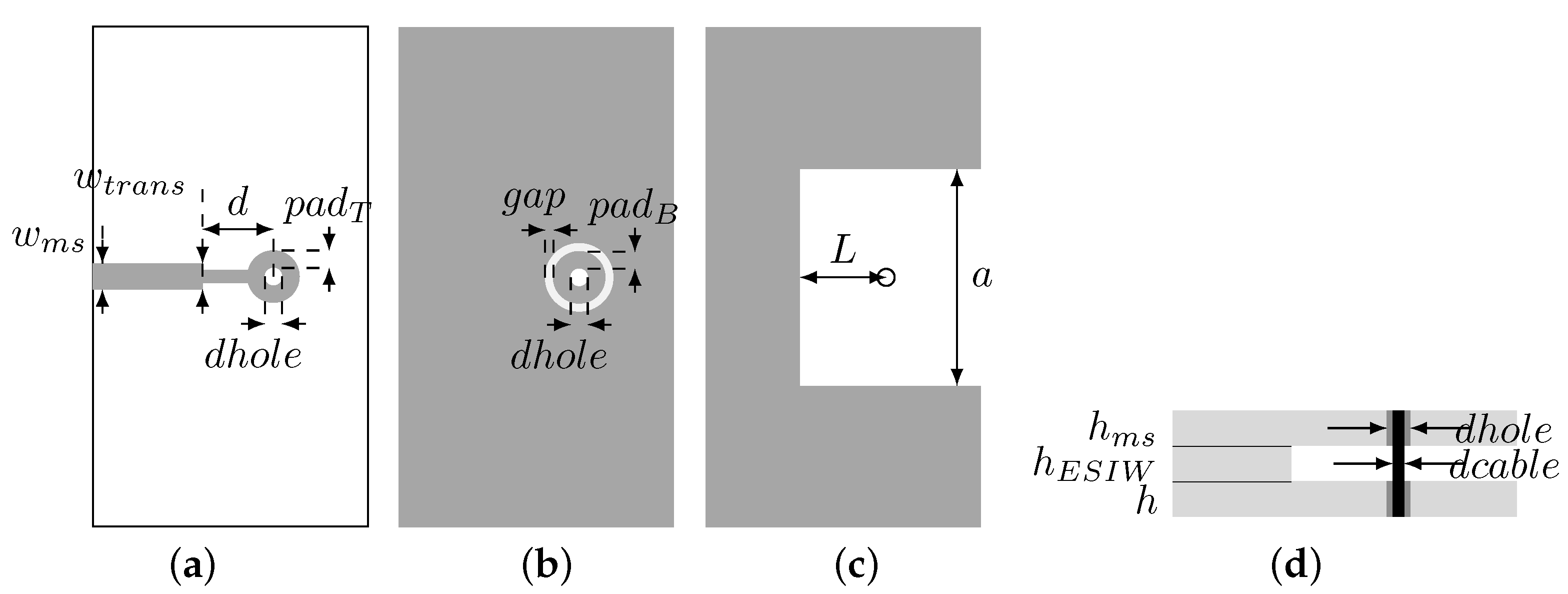
2. Design Method
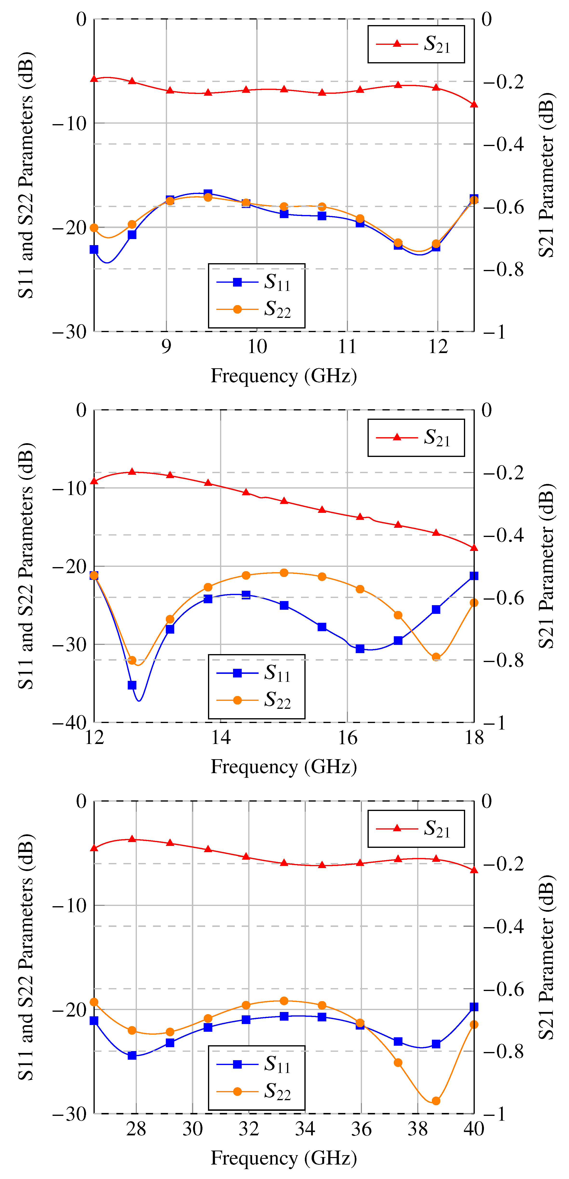
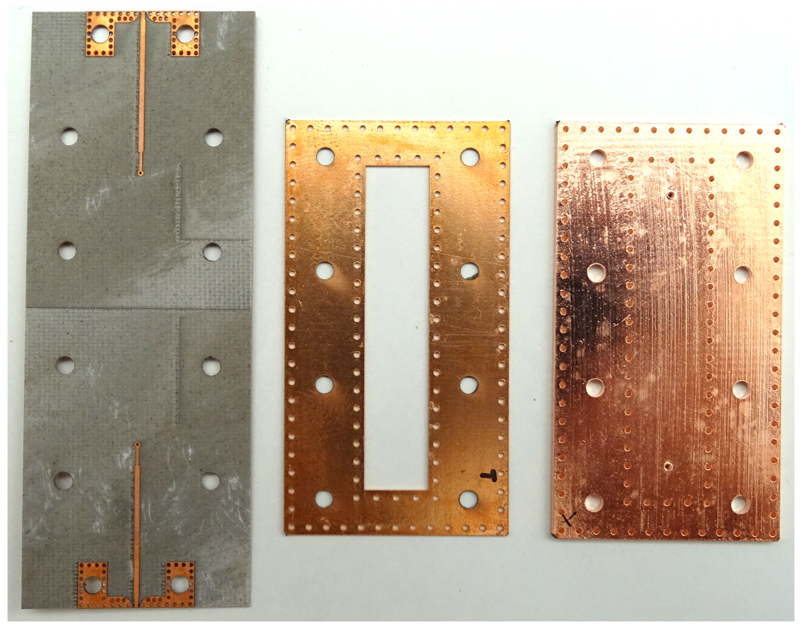
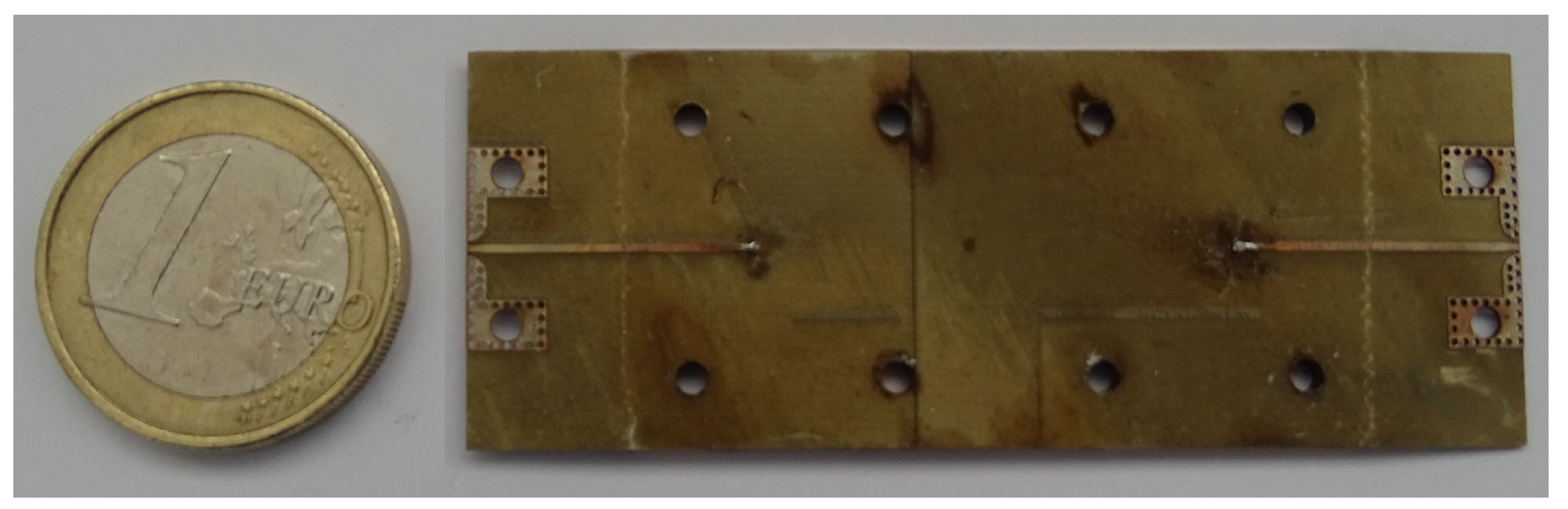
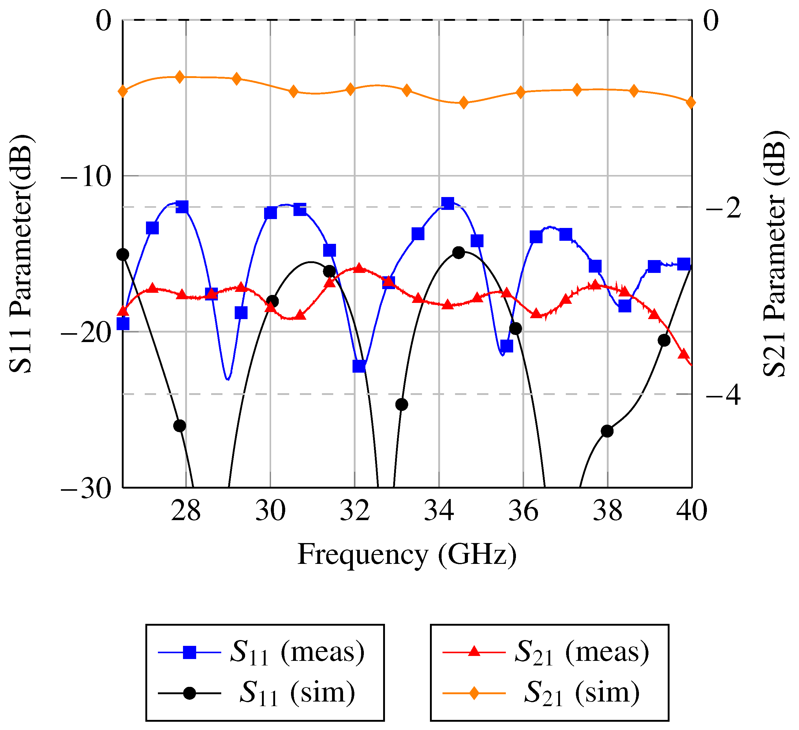
3. Results and Discussion
4. Conclusions
Author Contributions
Funding
Institutional Review Board Statement
Informed Consent Statement
Data Availability Statement
Conflicts of Interest
References
- Belenguer, A.; Esteban, H.; Boria, V.E. Novel Empty Substrate Integrated Waveguide for High-Performance Microwave Integrated Circuits. IEEE Trans. Microw. Theory Tech. 2014, 62, 832–839. [Google Scholar] [CrossRef]
- Deslandes, D.; Wu, K. Integrated microstrip and rectangular waveguide in planar form. IEEE Microw. Wireless Compon. Lett. 2001, 11, 68–70. [Google Scholar] [CrossRef]
- Belenguer, A.; Esteban, H.; Borja, A.; Ballesteros, J.; Fernandez, M.; Morro, J.; de Dios, J.; Bachiller, C.; Boria, V. Empty Substrate-Integrated Waveguides: A Low-Cost and Low-Profile Alternative for High-Performance Microwave Devices. In Wiley Encyclopedia of Electrical and Electronics Engineering; Wiley: New York, NY, USA, 2020; pp. 1–23. [Google Scholar] [CrossRef]
- Peng, H.; Xia, X.; Dong, J.; Yang, T. An improved broadband transition between microstrip and empty substrate integrated waveguide. Microw. Opt. Technol. Lett. 2016, 58, 2227–2231. [Google Scholar] [CrossRef]
- Esteban, H.; Belenguer, A.; Sanchez, J.R.; Bachiller, C.; Boria, V.E. Improved Low Reflection Transition from Microstrip Line to Empty Substrate-Integrated Waveguide. IEEE Microw. Wirel. Components Lett. 2017, 27, 685–687. [Google Scholar] [CrossRef]
- Liu, Z.; Xu, J.; Wang, W. Wideband Transition From Microstrip Line-to-Empty Substrate-Integrated Waveguide Without Sharp Dielectric Taper. IEEE Microw. Wirel. Components Lett. 2019, 29, 20–22. [Google Scholar] [CrossRef]
- Peng, H.; Zhao, F.; Liu, Y.; Tatu, S.O.; Yang, T. Robust Microstrip to Empty Substrate-Integrated Waveguide Transition Using Tapered Artificial Dielectric Slab Matrix. IEEE Microw. Wirel. Components Lett. 2020, 30, 849–852. [Google Scholar] [CrossRef]
- Ballesteros, J.A.; Belenguer, A.; Fernandez, M.D.; González, H.E.; Boria, V.E. Improved Microstrip-to-ESIW Transition with Elliptical Dielectric Taper in Ku-and Ka-Bands. IEEE Access 2022, 10, 51412–51418. [Google Scholar] [CrossRef]
- Belenguer, A.; Ballesteros, J.A.; Fernandez, M.D.; González, H.E.; Boria, V.E. Versatile, Error-Tolerant, and Easy to Manufacture Through-Wire Microstrip-to-ESIW Transition. IEEE Trans. Microw. Theory Tech. 2020, 68, 2243–2250. [Google Scholar] [CrossRef]
- Khan, A.A.; Kahar, M.; Mandal, M.K. A modified microstrip to empty substrate integrated waveguide transition. Int. J. Microw.-Comput.-Aided Eng. 2022, 32, e22990. [Google Scholar] [CrossRef]
- Morro, J.V.; Rodriguez, A.; Belenguer, A.; Esteban, H.; Boria, V. Multilevel transition in empty substrate integrated waveguide. Electron. Lett. 2016, 52, 1543–1544. [Google Scholar] [CrossRef]
- Ballesteros, J.A.; Fernandez, M.D.; Belenguer, A.; Esteban, H.; Boria, V.E. Versatile Transition for Multilayer Compact Devices in Empty Substrate Integrated Waveguide. IEEE Microw. Wirel. Components Lett. 2018, 28, 482–484. [Google Scholar] [CrossRef]
- Martínez, J.A.; Belenguer, A.; De Dios, J.J.; González, H.E.; Boria, V.E. Wideband Transition for Increased-Height Empty Substrate Integrated Waveguide. IEEE Access 2019, 7, 149406–149413. [Google Scholar] [CrossRef]
- Herraiz, D.; Martínez, L.; Ballesteros, J.A.; Fernandez, M.D.; Esteban, H.; Belenguer, Á. Manufacturing Methods Based on Planar Circuits. In Hybrid Planar-3D Waveguiding Technologies; IntechOpen: London, UK, 2022. [Google Scholar]
- Peng, H.; Xia, X.; Ovidiu Tatu, S.; Xu, K.; Dong, J.; Yang, T. Broadband phase shifters using comprehensive compensation method. Microw. Opt. Technol. Lett. 2017, 59, 766–770. [Google Scholar] [CrossRef]

| X-Band [9] | Ku-Band | Ka-Band | |
|---|---|---|---|
| (8.2–12.5 GHz) | (12–18 GHz) | (26.5–40 GHz) | |
| a | 22.86 | 15.7988 | 7.112 |
| L | 9.259 | 6.459 | 3.026 |
| 0.927 | 0.890 | 0.360 | |
| 0.264 | 0.559 | 0.184 | |
| 0.453 | 0.590 | 0.197 | |
| 0.612 | 0.740 | 0.216 | |
| d | 7.512 | 2.7863 | 2.306 |
| 0.51 | 0.51 | 0.21 | |
| 0.6 | 0.6 | 0.3 |
| X-Band [9] | Ku-Band | Ka-Band | |
|---|---|---|---|
| (8.2–12.5 GHz) | (12–18 GHz) | (26.5–40 GHz) | |
| Max. IL (dB) | 0.3 | 0.4 | 0.2 |
| Min. RL (dB) | 16.5 | 21.2 | 19.8 |
| Transition | Manufacturing | Freq. | IL Max | RL |
|---|---|---|---|---|
| Process | (GHz) | (dB) | (dB) | |
| [4] | medium | 12 | 1.5 | 13.5 |
| [5] | medium | 15 | 1.2 | 20 |
| [6] | easy | 15 | 1.08 | 21 |
| [7] | difficult | 33.25 | 1.26 | 14.7 |
| [8] | easy | 15 | 0.31 | 20.8 |
| [8] | easy | 33.25 | 1.36 | 14.75 |
| [9] | easy | 10.25 | 0.9 | 12 |
| [10] | easy | 10 | 1.3 | 15 |
| [15] | medium | 12 | 1.5 | 13.5 |
| This work | easy | 33.25 | 3.7 | 11.7 |
Disclaimer/Publisher’s Note: The statements, opinions and data contained in all publications are solely those of the individual author(s) and contributor(s) and not of MDPI and/or the editor(s). MDPI and/or the editor(s) disclaim responsibility for any injury to people or property resulting from any ideas, methods, instructions or products referred to in the content. |
© 2023 by the authors. Licensee MDPI, Basel, Switzerland. This article is an open access article distributed under the terms and conditions of the Creative Commons Attribution (CC BY) license (https://creativecommons.org/licenses/by/4.0/).
Share and Cite
Ballesteros, J.A.; Belenguer, A.; Fernandez, M.D.; Esteban, H.; Boria, V.E. Through-Wire Microstrip-to-Empty-Substrate-Integrated-Waveguide Transition at Ka-Band. Appl. Sci. 2023, 13, 9762. https://doi.org/10.3390/app13179762
Ballesteros JA, Belenguer A, Fernandez MD, Esteban H, Boria VE. Through-Wire Microstrip-to-Empty-Substrate-Integrated-Waveguide Transition at Ka-Band. Applied Sciences. 2023; 13(17):9762. https://doi.org/10.3390/app13179762
Chicago/Turabian StyleBallesteros, José A., Angel Belenguer, Marcos D. Fernandez, Hector Esteban, and Vicente E. Boria. 2023. "Through-Wire Microstrip-to-Empty-Substrate-Integrated-Waveguide Transition at Ka-Band" Applied Sciences 13, no. 17: 9762. https://doi.org/10.3390/app13179762